4, 💙💙 ☛ electronic ringer based on STM32 √★☆ 💙💙
Introduction
As a tool, the answerer has been widely used in various intelligence and knowledge contest occasions. However, the frequency of use of answering devices is low, and some of them are either complicated to make or have low reliability. As a unit, if you buy a responder, although it is economically affordable, it is used very rarely every year, and the responder (electronic device) is often damaged due to long-term storage, and the trouble and timeliness of repurchasing will affect The development of the activity, therefore designed this answering device.
introduction
As a tool, responder has been widely used in various intelligence and knowledge competitions. However, the use frequency of responders is low, and some are either complex or low reliability. As a unit, if a responder is specially purchased, although it is affordable economically, it is rarely used every year. The responder (of electronic devices) is often damaged due to long-term storage, and the trouble and timeliness of re purchase will affect the development of activities. Therefore, this responder is designed.
1. System overview
1.1 design tasks
Use STM32 to design an 8-way competition responder.
1.2 design requirements
-
(1) Eight players can answer at the same time by pressing the key;
-
(2) The answer time can be set by pressing the key;
-
(3) It can display the countdown time and show which player won;
-
(4) The referee may terminate the answer.
2. Scheme design and demonstration
2.1 chip selection scheme
The system uses single chip microcomputer STM32F103 as the control core. The system can complete the functions of operation control, signal recognition and display. Due to the use of single chip microcomputer, its technology is relatively mature, convenient and simple to apply, and there are few auxiliary circuits around the single chip microcomputer, which is easy to control and realize. The whole system has extremely flexible programmability, which can easily expand and change the functions of the system.
2.2 system overview
This design is based on the basic concept of eight way answer. Considering the function of setting time limit answer on demand, the rush answer system realized by STM32F103 single chip microcomputer and peripheral interface, and the principle of timer / counter timing and counting of single chip microcomputer, organically combine the software and hardware, so that the system can time correctly and the nixie tube can display the time correctly. Use the switch for keyboard output. At the same time, the system can realize: in the rush answer, the rush answer is valid only after the start. If the rush answer is invalid before the start of the rush answer; The limited time for answering questions and the time for answering questions can be set in 1-99s; It can show which contestant is effective and invalid; The countdown display of rush answer time and answer question time. When the system is full, the timing will be reset automatically and the master control will be reset forcibly; The key is locked. In the valid state, the key is invalid and illegal.
2.3 design requirements
-
① Eight players can answer at the same time by pressing the key;
-
② The answer time can be set by pressing the key;
-
③ It can display the countdown time and show which player wins.
-
④ The referee may terminate the answer.
2.4 overall system design idea
-
(1) Design a minimum hardware system of single chip microcomputer that can work normally, and the peripheral circuit includes setting the keyboard
-
(2) Software design, using the system clock of single chip microcomputer, first design a high-precision internal clock system, with a minimum accurate time of 1 second;
-
(3) A clock is designed based on the second counter, and the timing function is designed;
-
(4) Design interrupt function.
2.5 analysis of program implementation principle of each functional module
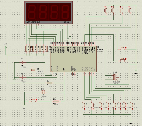
The module is composed of display module, LED module and button control module. And all of them are realized by STM32.
2.5. 1. Display module
The display passes P0 0/A00,P0. 1/A01,P0. 2/A0…P0.7/A07;P2.0/A8,P2.1/A9,P2.2/A10 these pins are connected to the chip. Combined with the key module, the state of the system is determined through the scanning function of single chip microcomputer, so as to display the corresponding data.
2.5. 2. Button control module
One end of the eight buttons is grounded respectively, and the other end is connected with the eight pins of one port of the single chip microcomputer for the contestants to answer. In addition, there are two buttons for the start and pause, which can be selected by the referee to start the pause. When the button is pressed, the corresponding pin changes from high level to low level, and then the single chip microcomputer scans and reads the level of the pin to judge whether the button is pressed. The other two buttons are start and pause,
2.5. 3. LED module
In the last 3 seconds of the countdown, the LED will flash to remind the contestant that the time is coming to an end.
3. STM32 performance introduction and hardware design
3.1 performance introduction of STM32 single chip microcomputer
STM32 has resources including 48KB SRAM, 256KB FLASH, 2 basic timers, 4 general timers, 2 advanced timers, 2 DMA controllers (12 channels in total), 3 SPI s, 2 IIC S, 5 serial ports, 1 USB, 1 CAN, 3 12 bit ADC s, 1 12 bit DAC, 1 SDIO interface and 51 general IO ports. The chip has high cost performance.
The description of each pin is as follows:
-
PA0 function 1, press KEY_UP 2 can be used as standby wake-up pin (WKUP) 3, and can be connected to DS18B20 sensor interface (P2 setting)
-
PA1 function 1, NRF24L01 interface IRQ signal 2, connected to HS0038 infrared receiver (P2 setting)
-
PA2 acts as the chip selection signal of W25Q64
-
PA3 acts as the chip selection pin of SD card interface
-
PA4 acts as CE signal of NRF24L01 interface
-
PA5 acts as SCK signal of W25Q64, SD card and NRF24L01 interface
-
PA6 acts as MISO signal of W25Q64, SD card and NRF24L01 interface
-
PA7 acts as MOSI signal of W25Q64, SD card and NRF24L01 interface
-
PA8 is used to connect DS0 LED lamp (red)
-
PA9 acts as TX pin of serial port 1, and is connected to RX of CH340 by default (P4 setting)
-
PA10 acts as RX pin of serial port 1, and is connected to TX(P4 setting) of CH340 by default
-
PA11 acts as a USB D-pin
-
PA12 acts as a USB D + pin
-
PA13 acts as JTAG/SWD simulation interface without any peripherals
-
PA14 acts as JTAG/SWD simulation interface without any peripherals
-
PA15 acts as 1, JTAG simulation port (JTDI) 2, CLK signal 3 of PS/2 interface, and connected to key 1
3.2 hardware design of electronic ringing system
The circuit diagram required for this procedure is as follows
4. System program
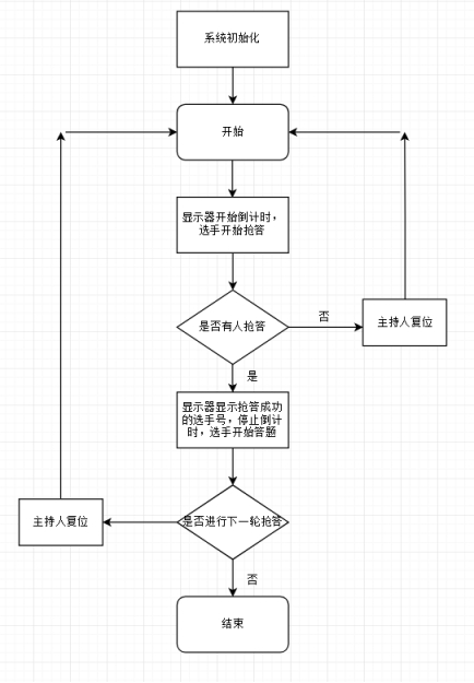
4.1. The main program design is as follows
The main program flow chart is shown in the figure below:
4.2 main program content
#include <stm32f10x_map.h>
#include <stm32f10x_type.h>
#include "lcd.h"
#include "sys.h"
#include "delay.h"
#include "usart.h"
#include "time.h"

u8 miao2;
u8 i;
const u32  smg_du[]={0xffd7,0xff11,0xffcd,0xff5d,0xff1b,0xff5e,0xffde,0xff15,0xffdf,0xff5f};
const u32  smg_wei[]={0xfffe,0xf7ff,0xfbff,0xfffd};
u8 flag=0;
u8 miao=60;
u8 flagc=0;

//main function
int main()
{
  Stm32_Clock_Init(9);
  delay_init(72);
  uart_init(72,9600);
  LCD_Init();
  Timerx_Init(1000,7199);
  AFIO->MAPR = 0x02000000;
  while(1)
   {
     if(flag==0)
	 {
         GPIOA->ODR=0xff08;
         GPIOB->ODR=0xf3fc;
         if(PCin(14)==0)
         {
             delay_ms(5);
             if(PCin(14)==0)
             {
                 flag=1;
                 i=0;
                 miao2=miao;
             }
         }
         if(PAin(13)==0)
         {
             delay_ms(5);
             if(PAin(13)==0)
             {
                 flag=2;
             }
             do
             {
                 while(PAin(13)==0);
                 delay_ms(10);
             }
             while(PAin(13)==0);
         }
     }
      if(flag==1)
      {
          GPIOB->ODR=smg_wei[0];
          GPIOA->ODR=smg_du[miao2%10];
          delay_ms(1);
          GPIOB->ODR=0xffff;

          GPIOB->ODR=smg_wei[1];
          GPIOA->ODR=smg_du[miao2/10];
          delay_ms(1);
          GPIOB->ODR=0xffff;
          if(PCin(15)==0)
          {
              delay_ms(5);
              if(PCin(15)==0)
              {
                  flag=4;
                  miao=miao2;
              }
          }
          if(PAin(13)==0)
          {
              delay_ms(5);
              if(PAin(13)==0)
              {
                  flag=5;
                  flagc=1;
                  i=0;
                  miao=miao2;
              }
          }
          if(PAin(15)==0)
          {
              delay_ms(5);
              if(PAin(15)==0)
              {
                  flag=5;
                  flagc=2;
                  i=0;
                  miao=miao2;
              }
          }
          if(PBin(4)==0)
          {
              delay_ms(10);
              if(PBin(4)==0)
              {
                  flag=5;
                  flagc=3;
                  i=0;
                  miao=miao2;
              }
          }
          if(PBin(5)==0)
          {
              delay_ms(10);
              if(PBin(5)==0)
              {
                  flag=5;
                  flagc=4;
                  i=0;
                  miao=miao2;
              }
          }
          if(PBin(6)==0)
          {
              delay_ms(10);
              if(PBin(6)==0)
              {
                  flag=5;
                  flagc=5;
                  i=0;
                  miao=miao2;
              }
          }
          if(PBin(7)==0)
          {
              delay_ms(10);
              if(PBin(7)==0)
              {
                  flag=5;
                  flagc=6;
                  i=0;
                  miao=miao2;
              }
          }
          if(PBin(8)==0)
          {
              delay_ms(10);
              if(PBin(8)==0)
              {
                  flag=5;
                  flagc=7;
                  i=0;
                  miao=miao2;
              }
          }
          if(PBin(9)==0)
          {
              delay_ms(10);
              if(PBin(9)==0)
              {
                  flag=5;
                  flagc=8;
                  i=0;
                  miao=miao2;
              }
          }
      }
      if(flag==2)
      {
          GPIOB->ODR=smg_wei[0];
          GPIOA->ODR=smg_du[miao%10];
          delay_ms(1);
          GPIOB->ODR=0xffff;

          GPIOB->ODR=smg_wei[1];
          GPIOA->ODR=smg_du[miao/10];
          delay_ms(1);
          GPIOB->ODR=0xffff;
          if(PAin(15)==0)
          {
              delay_ms(5);
              if(PAin(15)==0)
              {
                  do
                  {
                      while(PAin(15)==0);
                      delay_ms(10);
                  }
                  while(PAin(15)==0);
                  miao++;
              }
          }
          if(PBin(4)==0)
          {
              delay_ms(10);
              if(PBin(4)==0)
              {
                  do
                  {
                      while(PBin(4)==0);
                      delay_ms(10);
                  }
                  while(PBin(4)==0);
                  miao--;
              }
          }
          if(PAin(13)==0)
          {
              delay_ms(5);
              if(PAin(13)==0)
              {
                  flag=0;
              }
              do
              {
                  while(PAin(13)==0);
                  delay_ms(10);
              }
              while(PAin(13)==0);
          }
      }
      if(flag==4)
      {
          GPIOB->ODR=smg_wei[0];
          GPIOA->ODR=smg_du[miao%10];
          delay_ms(1);
          GPIOB->ODR=0xffff;

          GPIOB->ODR=smg_wei[1];
          GPIOA->ODR=smg_du[miao/10];
          delay_ms(1);
          GPIOB->ODR=0xffff;
          if(PCin(14)==0)
          {
              delay_ms(5);
              if(PCin(14)==0)
              {
                  flag=1;
                  i=0;
                  miao2=miao;
              }
          }
      }
      if(flag==3)
      {
          GPIOB->ODR=0xffff;
      }
      if(flag==5)
      {
          GPIOB->ODR=smg_wei[0];
          GPIOA->ODR=smg_du[miao%10];
          delay_ms(1);
          GPIOB->ODR=0xffff;

          GPIOB->ODR=smg_wei[1];
          GPIOA->ODR=smg_du[miao/10];
          delay_ms(1);
          GPIOB->ODR=0xffff;

          GPIOB->ODR=smg_wei[2];
          GPIOA->ODR=0xff08;
          delay_ms(1);
          GPIOB->ODR=0xffff;

          GPIOB->ODR=smg_wei[3];
          GPIOA->ODR=smg_du[flagc];
          delay_ms(1);
          GPIOB->ODR=0xffff;
      }
  }
}
4.3 timer interrupt function and key program
#include "time.h"
#include <stm32f10x_map.h>
#include <stm32f10x_nvic.h>
void TIM3_IRQHandler(void)
{
    if(TIM3->SR&0X0001)
    {	if((i%10==5)&&(flag==1)&&(miao2<=5))
        GPIOC->ODR=0xdfff;
     else GPIOC->ODR=0xffff;

     if(i>=9)
     {
         if((miao2==0)&&(flag==1))
         {
             miao2=0;
             flag=3;
         }
         i=0;
         miao2--;

     }
     i++;
    }
    TIM3->SR&=~(1<<0);
}

void Timerx_Init(u16 arr,u16 psc)
{
    RCC->APB1ENR|=1<<1;
    TIM3->ARR=arr;
    TIM3->PSC=psc;

    TIM3->DIER|=1<<0;
    TIM3->DIER|=1<<6;
    TIM3->CR1|=0x01;
    MY_NVIC_Init(1,3,TIM3_IRQChannel,2);
}
4.3 LCD program
#include "lcd.h"
#include "delay.h"
#include "sys.h"

u16 POINT_COLOR = 0x0000,BACK_COLOR = 0xFFFF;
u16 DeviceCode;

void LCD_WR_REG(u16 data)
{
	LCD_RS_CLR;
 	LCD_CS_CLR;
	DATAOUT(data);
	LCD_WR_CLR;
	LCD_WR_SET;
 	LCD_CS_SET;
}


void LCD_WriteReg(u8 LCD_Reg, u16 LCD_RegValue)
{
	LCD_WR_REG(LCD_Reg);
	LCD_WR_DATA(LCD_RegValue);
}

u16 LCD_ReadReg(u8 LCD_Reg)
{
	u16 t;
	LCD_WR_REG(LCD_Reg);
	GPIOE->CRL=0X88888888;
	GPIOE->CRH=0X88888888;
	GPIOE->ODR=0XFFFF;

	LCD_RS_SET;
	LCD_CS_CLR;

	LCD_RD_CLR;
	delay_us(5);
	LCD_RD_SET;
	t=DATAIN;
	LCD_CS_SET;
    GPIOE->CRL=0X33333333;
	GPIOE->CRH=0X33333333;
	GPIOE->ODR=0XFFFF;
	return t;
}

void LCD_WriteRAM_Prepare(void)
{
	LCD_WR_REG(R34);
}

void LCD_WriteRAM(u16 RGB_Code)
{
	LCD_WR_DATA(RGB_Code);
}

u16 LCD_BGR2RGB(u16 c)
{
  u16  r,g,b,rgb;
  b=(c>>0)&0x1f;
  g=(c>>5)&0x3f;
  r=(c>>11)&0x1f;
  rgb=(b<<11)+(g<<5)+(r<<0);
  return(rgb);
}

u16 LCD_ReadPoint(u16 x,u16 y)
{
	u16 t;
	if(x>=LCD_W||y>=LCD_H)return 0;
	LCD_SetCursor(x,y);
	LCD_WR_REG(R34);
	GPIOE->CRL=0X88888888;
	GPIOE->CRH=0X88888888;
	GPIOE->ODR=0XFFFF;

	LCD_RS_SET;
	LCD_CS_CLR;
	LCD_RD_CLR;
	LCD_RD_SET;
	delay_us(2);
	LCD_RD_CLR;
	delay_us(2);
	LCD_RD_SET;
	t=DATAIN;
	LCD_CS_SET;

	GPIOE->CRL=0X33333333;
	GPIOE->CRH=0X33333333;
	GPIOE->ODR=0XFFFF;
	if(DeviceCode==0X4531||DeviceCode==0X8989)return t;
	else return LCD_BGR2RGB(t);
}

void LCD_DisplayOn(void)
{
	LCD_WriteReg(R7, 0x0173);
}
void LCD_DisplayOff(void)
{
	LCD_WriteReg(R7, 0x0);
}

void LCD_SetCursor(u16 Xpos, u16 Ypos)
{
#ifdef USE_HORIZONTAL
	if(DeviceCode==0X8989)
	{
		LCD_WriteReg(0X4E, Ypos);
		LCD_WriteReg(0X4F, 319-Xpos);
    }else
	{
		LCD_WriteReg(R32, Ypos);
		LCD_WriteReg(R33, 319-Xpos);
	}
#else
	if(DeviceCode==0X8989)
	{
		LCD_WriteReg(0X4E, Xpos);
		LCD_WriteReg(0X4F, Ypos);
    }else
	{
		LCD_WriteReg(R32, Xpos);
		LCD_WriteReg(R33, Ypos);
	}
#endif
}
void LCD_Init(void)
{
    RCC->APB2ENR|=1<<2;
    RCC->APB2ENR|=1<<3;
    RCC->APB2ENR|=1<<4;
	GPIOA->CRL&=0X00000000;
	GPIOA->CRL|=0X33333333;

	GPIOA->CRH=0X88888888;

	GPIOA->ODR=0xFFFF;

    GPIOB->CRH&=0X00000000;
	GPIOB->CRH|=0X88883388;

	GPIOB->CRL&=0X00000000;
	GPIOB->CRL|=0X88888333;
    GPIOB->ODR=0Xffff;


	GPIOC->CRH&=0X00000000;
	GPIOC->CRH|=0X88388888;
	GPIOC->ODR=0Xffff;

}

void LCD_setwindow(unsigned char x0,unsigned int y0,unsigned char x1,unsigned int y1)
{
   LCD_WriteReg(0x20, x0);
   LCD_WriteReg(0x21, y0);
   LCD_WriteReg(0x0050, x0);
   LCD_WriteReg(0x0051, x1);
   LCD_WriteReg(0x0052, y0);
   LCD_WriteReg(0x0053, y1);
   LCD_WR_REG(0x0022);
}

u16 RGB(u8 R,u8 G,u8 B)
{
	return((u16)(R&0XF8)<<8|(u16)(G&0XFC)<<3|(u16)(B&0XF8)>>3);
}
5. System debugging and analysis
5.1 system commissioning
The debugging of the system mainly uses the joint debugging of software and hardware to check whether there are problems and where there are problems in the responder. Because the module design method is adopted in the system design, it is convenient to test the functions of each circuit module level by level: case module debugging, data modification module debugging, display module debugging, etc.
5.2 commissioning phenomenon and analysis
After the power is turned on, each module can be debugged. For example, debug the key module. We press the start button, stop button and rush answer button to observe the display to realize the start, stop and rush answer function. If any key fails to realize the corresponding function after being pressed, it proves that there may be a problem with the key module, of course, there may be a problem with the program, and there may be a problem with the construction of the simulation diagram. At this time, the program can be debugged by simulation software. If there is no error in the construction of the simulation diagram, if the simulation cannot be performed normally, it is proved that there is a problem in the program, which may be the problem of the key subroutine or the error of the main program. If it can simulate normally, it proves that there is a problem with the hardware key module. It may be due to poor welding of key pins, damage of key parts, etc. Other modules are the same. You need to be patient to eliminate the possibility of various errors one by one.
5.3 test results
The normal phenomenon should be to turn on the power supply. At this time, press the rush answer buttons No. 2 and No. 3 to adjust the rush answer time. Press the start button, and the display shows the countdown to start answering. Press the answer button, the display displays the number of the contestant who has successfully answered the answer, and stop the countdown. At the same time, in case of special circumstances, press the stop key to stop answering.
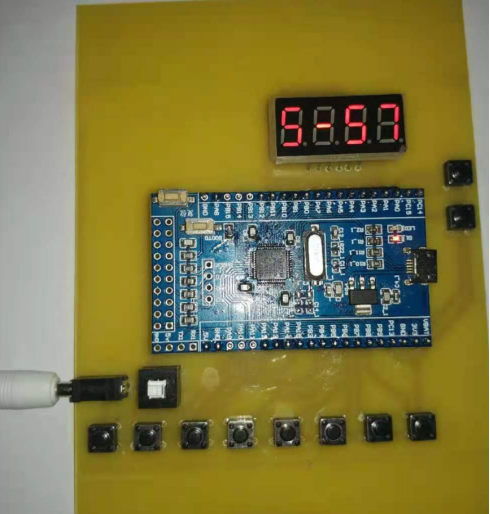
The effect of this system is very good, and it can realize the content specified by the design requirements and purposes.