4.5 DS18B20 temperature sensor
4.5.1 introduction to schematic diagram
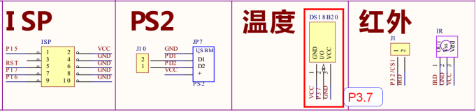
Figure 4-5-1
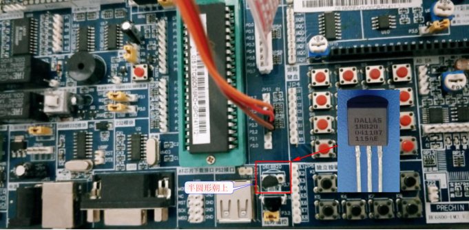
Figure 4-5-2
The DS18B20 module on the experimental board is connected to P3.5 of MCU On the IO port, when inserting the DS18B20 chip, the arc is inserted upward. See the above picture for the specific effect.
4.5.2 introduction to DS18B20 temperature sensor
DS18B20 is a commonly used digital temperature sensor. Its output is digital signal. Its temperature detection and digital data output are integrated on one chip, so it has stronger anti-interference ability.
The main features of DS18B20 are as follows:
(1) Full digital temperature conversion and output.
(2) Advanced single bus data communication. (one line can collect temperature)
(3) The maximum resolution is 12 bits, and the accuracy can reach 0.5 ℃.
(4) The maximum working cycle at 12 bit resolution is 750 milliseconds.
(5) . parasitic working mode can be selected.
(6) The detection temperature range is – 55 ° C ~+125 ° C (– 67 ° F ~+257 ° F)
(7) Built in EEPROM, temperature limit alarm function.
(8) 64 bit lithography ROM with built-in product serial number to facilitate multi machine connection. (support one line to operate multiple chips)
(9) Various packaging forms are suitable for different hardware systems. See the following pictures for packaging.
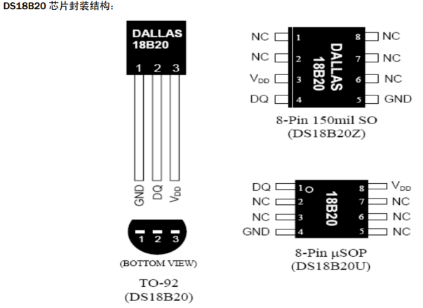
Figure 4-5-3
Pin functions of the chip in the picture: GND voltage ground, DQ single data bus, VDD power supply voltage, NC empty pin
4.5.3 Introduction to the working principle of DS18B20
The temperature detection and digital data output of DS18B20 are integrated on one chip, so the anti-interference power is stronger.
Its working cycle can be divided into two parts, temperature detection and data processing.
There are three types of memory in DS18B20:
(1) ROM read only memory: it is used to store DS18B20ID code. The first 8 bits are single line series code (DS18B20 code is 19H), the last 48 bits are the unique serial number of the chip, and the last 8 bits are CRC code (redundancy check) of more than 56 bits. The data can not be changed by the user when the chip leaves the factory. DS18B20 has 64 bit ROM(8+48+8).
(2) RAM data register: used for internal calculation and data access. Data is lost after power failure. DS18B20 has 9 bytes of ram, and each byte is 8 bits. The first and second bytes are the data value information after temperature conversion, and the third and fourth bytes are the image of user EEPROM (commonly used for temperature alarm value storage). Its value will be refreshed during power on reset. The fifth byte is the image of the user's third EEPROM. The 6th, 7th and 8th bytes are count registers, which are designed to allow users to obtain higher temperature resolution. They are also temporary storage units for internal temperature conversion and calculation. The 9th byte is the CRC code of the first 8 bytes.
(3) EEPROM nonvolatile memory: used to store data that needs to be saved for a long time. For example: For the upper and lower temperature alarm values and verification data, DS18B20 has a total of 3 bytes of EEPROM, and there are images in RAM to facilitate user operation.
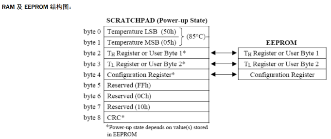
Figure 4-5-4
DS18B20 works in 12 bit resolution mode by default. The converted 12 bit data is stored in two 8-bit RAM of DS18B20 (the first two bytes). The first five bits in binary are symbol bits. If the measured temperature is greater than 0, these five bits are 0. As long as the measured value is multiplied by 0.0625, the actual temperature can be obtained; If the temperature is less than 0, the five digits are 1. The measured value needs to be inversely added by 1 and multiplied by 0.0625 to obtain the actual temperature.
Bit operation can also be used for data extraction. The read data is 2 bytes, with a total of 16 bits (H and L). The lowest 4 bits are decimal digits, and the rest are integer digits. If the read data is negative, you need - 1 to get the real data.
For example:
int temp=0;
temp=DS18B20_ReadTemp(); //Read the temperature collected by DS18B20 once (return to H+L bit)
if(temp<0) //If the temperature is negative
{
    temp=temp-1;
    temp=~temp;
    printf("DS18b20=-%d.%d\r\n",temp>>4,temp&0xF);
}
else
{
printf("DS18b20=%d.%d\r\n",temp>>4,temp&0xF);
}
4.5.4 Introduction of common instructions for DS18B20 operating ROM/RAM
1. Read 64 bit ROM encoding instruction: 0x33
This command allows the bus controller to read the 64 bit ROM of the DS18B20. This instruction can only be used when there is only one DS18B20 on the bus. If more than one DS18B20 is attached, data conflict will occur during communication.
2. Matching chip instruction: 0x55
This command is followed by the 64 bit serial number issued by the controller. When there are multiple DS18B20 on the bus, only the chip with the same serial number issued by the control can respond, and other chips will wait for the next reset. This instruction is suitable for single chip and multi chip hooking.
3. Skip ROM code matching: 0xCC
This instruction makes the chip not respond to ROM coding. In the case of single bus, this instruction can be selected in order to save time. If this instruction is used during multi chip attach, data conflict will occur, resulting in an error.
4. Start temperature conversion: 0x44
After receiving this command, the chip will perform a temperature conversion and put the converted temperature value into the first and second addresses of RAM. After that, because the chip is busy with temperature conversion processing, when the controller sends a read time slot, the bus will output "0", and when the storage work is completed, the bus will output "1". In the parasitic working mode, the chip must be pulled up immediately after issuing this command and maintained for at least 500MS to maintain the operation of the chip.
5. Read data instruction from RAM: 0xBE
This instruction will read data from RAM. The read address starts from address 0 and can be read to address 9 to complete the reading of the whole ram data. The chip allows to stop reading with a reset signal during reading, that is, it can not read the following unnecessary bytes to reduce the reading time.
4.5.5 DS18B20 sequence diagram
(1). DS18B20 reset and response sequence diagram
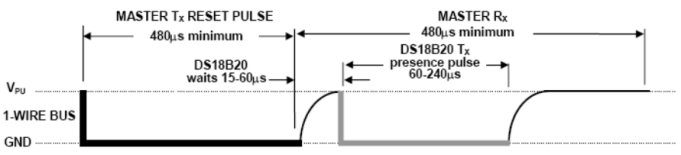
Figure 4-5-5 reset and response sequence diagram
Figure 4-5-6
Reset must be carried out before each communication with DS18B20. The reset time, waiting time and response time shall be programmed in strict accordance with the sequence.
(2) Write data timing
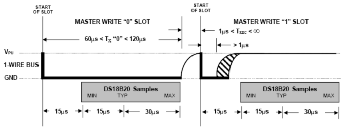
Figure 4-5-7 data writing sequence diagram
The above timing diagram is the timing diagram for writing data to DS18B20. The diagram is divided into two parts. The left part is the timing diagram for transmitting data 0 and the right part is the timing diagram for transmitting data 1.
According to the prompt of the sequence diagram (the right part), before sending data each time (whether data 0 or data 1), it is necessary to lower the bus by at least 1us.
If the data to be sent next is 0, the data line needs to be pulled down for at least 60us, and the sampling time of DS18B20 to the bus is within 15~60us; During the sampling time, if the bus is low, it means to write 0, and if the bus is high, it means to write 1.
If the data to be sent next is 1, it is also necessary to pull down the data line for at least 60us, and the sampling time of DS18B20 to the bus is within 15~60us; During the sampling time, if the bus is low, it means to write 0, and if the bus is high, it means to write 1.
Note: during communication, it is transmitted to DS18B20 in a byte unit, and the byte reading or writing starts from the low bit.
(3) Read data timing
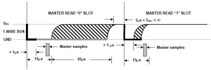
Fig. 4-5-8 data reading sequence diagram
The above timing diagram is a timing diagram for reading data from DS18B20. The diagram is divided into two parts. The left part is the bus level change process when reading data 0, and the right part is the bus level change process when reading data 1.
According to the prompt of the timing chart (right part), before reading data (whether data 0 or data 1), the bus needs to be pulled down by the host for at least 1us, and then release the bus (pulled up);
Then it needs to wait for 15us before the bus data can be read. DS18B20 will maintain the bus level in the following 45us, during which the data read from the bus is valid data.
be careful: After the bus is pulled down by 1us, the bus data can be read only after 15us, so as to ensure that the bus data is accurate.
In the communication process, the data output by DS18B20 is transmitted from the low bit.
4.5.6 steps for reading temperature
Scenario where there is only a single DS18B20 on the bus (read the temperature of DS18B20 once):
one Send reset pulse to the bus and detect the response signal of DS18B20 (it can ensure that there is no problem with DS18B20 hardware)
two Send instruction to skip ROM number check (instruction 0xCC)
three Send temperature conversion command (command 0x44)
(during the temperature conversion process of DS18B20, the bus will always maintain a high level state and will not respond to the bus command)
four Send reset pulse to the bus and detect the response signal of DS18B20
five Send instruction to skip ROM number check (instruction 0xCC)
six Send command to read temperature (command 0xBE)
seven Then read the lower 8 bits of temperature data
eight Then read the high 8 bits of temperature data
4.5.7 read DS18B20 temperature example code (single DS18B20 scenario)
The following code demonstrates the process of cyclically reading the temperature of DS18B20. Read the temperature once every 1 second in the main function.
Pay attention to time control when writing DS18B20 timing code.
The current environment of the experimental board: the STC90C516RD single chip microcomputer is adopted, the crystal oscillator is 12MHZ, works in 12T mode, and the time consumed by executing an i + + statement in the code is about 12us. The delay time in the program is calculated through this time. If the program is to be transplanted to other MCU, pay attention to the problem of time.
(description of hardware platform: CPU is STC90C516RD, crystal oscillator frequency is 12MHZ, working in 12T mode, and one machine cycle is 1us time)
Example code:
#include <reg51.h>
/*DS18B20 Hardware interface:   P3.5*/
sbit DS18B20_GPIO=P3^7;
int DS18B20_ReadTemp(void);
/*
explain:   In 12MHZ crystal oscillator and 12T mode, the time consumed by i + + is almost 12us
*/
/*
Function name: u8   DS18B20_Init(void)
Function: send reset pulse to DS18B20 and detect response signal
 return   return   Values: 1 indicates failure, 0 indicates success
 explain:   51 MCU IO port default output high level
*/
u8 DS18B20_ResetSignal(void)
{
    u8 i=0;
    //one   Send reset signal
    DS18B20_GPIO=0;//Pull the bus down 480us
    i=50;
    while(i--){}   //Delay 600us  , 480us minimum
    i=0;
    DS18B20_GPIO=1;//Then release (pull up) the bus. If the DS18B20 reacts, it will pull down the bus after 15us~60us
    //two   Wait for DS18B20 to pull down the bus
    while(DS18B20_GPIO)
    {
        i++;
        if(i>10)return 1;//fail  , About 120us
    }
    //three   Wait for DS18B20 to release the bus
    i=0;
    while(DS18B20_GPIO==0) //60us~240us
    {
        i++;
        if(i>20)return 1;//Failed, about 240us
    }
    return 0;//Initialization succeeded
}
/*
Function name: u8   DS18B20_WriteByte(void)
Function: write one byte of data to DS18B20
 Function parameter: byte data written
*/
void DS18B20_WriteByte(u8 byte)
{
    u16 i=0,j=0;
    for(j=0;j<8;j++)
    {
        DS18B20_GPIO=0;//Pull the bus down 1us before writing a bit of data
        i++; //+1 the time consumed is 12us
        DS18B20_GPIO=byte&0x01;//Then write a data, starting from the lowest bit
        i=6;
        while(i--){}//The duration is at least 60us, about 72us here
        DS18B20_GPIO=1;//Then release the bus
        byte>>=1;//Continue sending
    }
}
/*
Function name: u8   DS18B20_ReadByte(void)
Function: read one byte of data from DS18B20
 return   return   Value: read data
*/
u8 DS18B20_ReadByte(void)
{
    u8 byte=0;
    u16 i=0,j=0;
    for(j=0;j<8;j++)
    {
        DS18B20_GPIO=0;//Pull the bus down 1us first
        i++;//+1 the time consumed is 12us
        DS18B20_GPIO=1;//Then release the bus
        i++;
        i++;//Wait at least 15us before reading data
        byte>>=1; //Start receiving data from the low bit
        if(DS18B20_GPIO)byte|=0x80;
        i=4; //After reading, wait 48us before reading the next data
        while(i--){}
    }
    return byte;
}
/*
Function name: u16   DS18B20_ReadTemp(void)
Function: read the temperature data of DS18B20 once
 return   return   Value: read temperature value
 be careful:   The return value should use a signed data type because the temperature can return a negative number.
*/
int DS18B20_ReadTemp(void)
{
    int temp=0;//Store temperature data
    u8 TH,TL;
    //Step 1:   Start temperature conversion
    DS18B20_ResetSignal(); //Send reset pulse and detect response signal
    DS18B20_WriteByte(0xcc);//Skip ROM operation command
    DS18B20_WriteByte(0x44);//Temperature conversion command

    //Step 2:   Read temperature
    DS18B20_ResetSignal();//Send reset pulse and detect response signal
    DS18B20_WriteByte(0xcc);//Skip ROM operation command
    DS18B20_WriteByte(0xbe);//Send read temperature command
    TL=DS18B20_ReadByte();//Read the temperature value, 16 bits in total, and read the low byte first
    TH=DS18B20_ReadByte();//Reread high byte
    temp=TH<<8|TL; //Merge into 16 bits
    return temp;
}
int main()
{
    int temp=0;
    UART_Init();        //The baud rate of initialization serial port is 4800
    while(1)
    {
        temp=DS18B20_ReadTemp();
        if(temp<0) //If the temperature is negative
        {
            temp=temp-1;
            temp=~temp;
            printf("DS18b20=-%d.%d\r\n",temp>>4,temp&0xF);
        }
        else
        {
            printf("DS18b20=%d.%d\r\n",temp>>4,temp&0xF);
        }
        DelayMs(1000);
}
}