Puzhong 51-mononuclear-A2
STC89C52
Keil uVision V5.29.0.0
PK51 Prof.Developers Kit Version:9.60.0.0
Upper computer: Vofa+ 1.3.10
Hard knowledge
Excerpt from "development strategy of Puzhong 51 single chip microcomputer" and "DS1302 Chinese manual".
Introduction to DS1302
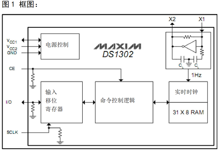
DS1302 is a trickle charging clock chip launched by DALLAS company. It contains a real-time clock / calendar and 31 byte static RAM. It communicates with MCU through a simple serial interface. The real-time clock / calendar circuit provides the information of seconds, minutes, hours, days, weeks, months and years. The days of each month and leap years can be automatically adjusted. Clock operation can be determined in 24 or 12 hour format through AM/PM instruction. DS1302 and MCU can simply communicate in synchronous serial mode, and only three communication lines are required:
① RES reset
② I/O data cable
③ SCLK serial clock.
The read / write data of the clock / RAM is communicated in one byte or a character group of up to 31 bytes. DS1302 has low power consumption when working, and the power is less than 1mW when maintaining data and clock information. DS1302 is improved from DS1202 and the following features are added: dual power pins are used for main power supply and backup power supply, Vcc1 is a programmable trickle charging power supply, and seven byte memory is added. It is widely used in telephone, fax, portable instrument, battery powered instrument and other product fields.
Main performance indicators:
★ the real-time clock has the ability to calculate seconds, minutes, hours, days, weeks, months and years before 2100, as well as the ability to adjust in leap years; ★ 31 8-bit temporary data storage RAM;
★ the serial I/O port mode minimizes the number of pins;
★ wide range working voltage: 2.0 ~ 5.5V;
★ when working at 2.0V, the current is less than 300nA;
★ when reading / writing clock or RAM data, there are two transmission modes: single byte transmission and multi byte transmission character group;
★ 8-pin DIP package or optional 8-pin SOIC package shall be assembled according to the surface;
★ simple 3-wire interface;
★ compatible with TTL, Vcc=5V;
★ optional industrial grade temperature range - 40 ~ + 85;
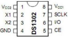
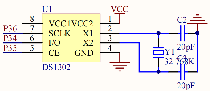
- VCC2: main power pin
- X1 and X2: DS1302 external crystal oscillator pins, which usually need to be externally connected with 32.768K crystal oscillator
- GND: power ground
- CE: the enable pin is also the reset pin (the function of the new version is changed).
- I/O: serial data pin, data output or input from this pin
- SCLK: serial clock pin
- VCC1: standby power supply
DS1302 use
The general process of operating DS1302 is to write various data into the register of DS1302 to set its current time format. Then make the DS1302 start to operate, the DS1302 clock will operate according to the setting, and then the single chip microcomputer will read out the data in its register. Liquid crystal display is what we often call a simple electronic clock. Therefore, generally speaking, the operation of DS1302 is divided into two steps (the display part belongs to the content of liquid crystal display, not the content of DS1302 itself). However, before describing the operation sequence, we should first look at the register. DS1302 has a control register, 12 calendars, clock registers and 31 RAM.

Control register
The control register is used to store the control command word of DS1302. The first byte written after the RST pin of DS1302 returns to the high level is the control command. It is used to control the reading and writing process of DS1302. The format is as follows:
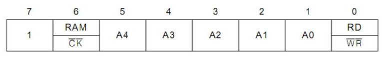
The above figure shows the register style of DS1302. We can see:
- The seventh is always 1;
- Bit 6, 1 indicates RAM, addressing internal memory address; 0 indicates CK, addressing the internal register;
- Bits 5 to 1 are RAM or register addresses;
- The lowest level and high level indicate RD, that is, the next operation will be "read"; Low level indicates W, that is, the next operation will be "write".
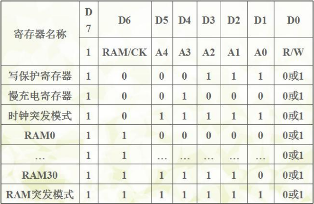
For example, if you want to read the second register, the command is 1000 0001, otherwise it is written as 1000 0000.
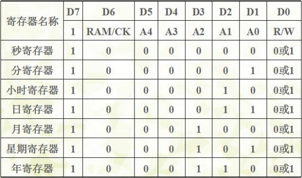
Calendar / clock register
DS1302 has 12 registers, of which 7 are related to calendar and clock, and the stored data is in the form of BCD code. The format is as follows:

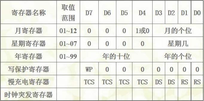
Second register: the lower four bits are one bit of second, and the higher three bits are ten bits of second. The highest CH is the operation flag of DS1302. When CH=0, the internal clock of DS1302 runs, otherwise, it stops when CH=1;
Hour register: hour register. The highest bit is the 12 / 24-hour format selection bit. When this bit is 1, it indicates the 12-hour format. When set to 12 hour display format, the high level of bit 5 indicates afternoon (PM); When it is set to 24-hour format, the fifth bit is the specific time data.
Write protection register: when the highest WP of the register is 1, DS1302 is read-only and does not write, so ensure that WP is 0 before writing data to DS1302.
Slow charging register (trickle current charging) register: we know that when the DS1302 is powered down, the external power supply protection time data can be called immediately. This register is used to configure the charging option of the standby power supply. The upper four bits (4 TCS s) can only use the charging option under the condition of 1010; The lower four bits are related to the internal circuit of DS1302.
In the calendar / clock register, data is stored in BCD code, which represents the 10 numbers 0 ~ 9 in 1-bit decimal system through 4-bit binary code. As follows:

Read and write timing of DS1302
At the rising edge of the next SCLK clock after the control instruction word input, the data is written to DS1302, and the data input starts from the low bit (bit 0). Similarly, the data of DS1302 is read out on the falling edge of the next SCLK pulse immediately following the 8-bit control command word, and the data is read out from low bit 0 to high bit 7. The sequence diagram is as follows:

The above figure shows the three timing of DS1302: reset timing, single byte write timing and single byte read timing;
CE (RST): reset sequence, that is, a positive pulse is generated at the rst pin. RST should maintain high level in the whole reading and writing device. After reading and writing a byte, pay attention to returning RST to low level to prepare for the next reading and writing cycle;
Single byte read timing: note that before reading, write the command to the register first, starting from the lowest bit; It can be seen that writing data is implemented on the rising edge of SCLK, while reading data is implemented on the falling edge of SCLK. Therefore, in the single byte read sequence, the eighth falling edge immediately after the end of the eighth rising edge of the write command will read the first bit data of the register to be read to the data line! This is the most special part of DS1302 operation. Of course, the data read out also starts from the lowest point.
Single byte write timing: two bytes of data can be written with 16 rising edges.
Procedure precautions:
★ remember to turn off write protection before operating DS1302;
★ pay attention to reducing the speed of single chip microcomputer with time delay to match the device timing;
★ the data read out by DS1302 is in the form of BCD code, which should be converted into our customary decimal system. The conversion method is in the source program;
★ before reading bytes, set IO as the input port, and after reading, change it back to the output port;
★ when writing a program, it is recommended to open up an array (memory space) to centrally place a series of data of DS1302, which is convenient for expanding keyboard input in the future.
circuit design
Sample program
stdint.h see [51 single chip microcomputer quick start guide] 1: basic knowledge and engineering creation
See for software SPI program [51 MCU quick start guide] 5: software SPI
For serial port, see [51 MCU quick start guide] 3.3: USART serial communication
DS1302.c
#include "./Software_SPI/Software_SPI.h"
#include <STC89C5xRC.H>
#include "DS1302.h"

sbit DS1302_CS = P3^5;

//DS1302_ It needs to be modified when CS is pulled up and transplanted
void DS1302_CS_H()
{
	DS1302_CS = 1;
}

//DS1302_CS is pulled down and needs to be modified during transplantation
void DS1302_CS_L()
{
	DS1302_CS = 0;
}

//---The storage order is seconds, minutes, hours, days, months and anniversaries---//
uint8_t gDS1302_TIME[7] = {0};

//---DS1302 address command for writing hours, minutes and seconds---//
//---Second minute hour Sun Moon anniversary-------//
code uint8_t gWRITE_RTC_ADDR[7] = {0x1, 0x41, 0x21, 0x61, 0x11, 0x51, 0x31};

/*******************************************************************************
Num2BCD
 Digital to BCD code (two digits)
*******************************************************************************/
#define Num2BCD(value) (((value/10)<<4)|(value%10))

/*******************************************************************************
* Function name: reversed
* Function function 		 :  One byte in reverse order
*******************************************************************************/
uint8_t reversed(uint8_t raw)
{
	uint8_t i, value = 0;
	for(i = 0; i < 8; i++)
	{
		value <<= 1;
		value |= (raw & 0x01);
		raw >>= 1;
	}
	return value;
}

/*******************************************************************************
* Function name: ds1302_write_byte
* Function function 		 :  DS1302 write single byte
* Input: addr: Address / command
				   dat: data
* Output 	 :  nothing
*******************************************************************************/
void ds1302_write_byte(uint8_t addr,uint8_t dat)
{
	DS1302_CS_L();
	DS1302_CS_H();

	SOFT_SPI_RW_MODE0(addr);
	SOFT_SPI_RW_MODE0(dat);

	DS1302_CS_L();
}

/*******************************************************************************
* Function name: ds1302_read_byte
* Function function 		 :  DS1302 read single byte
* Input: addr: Address / command
* Output 	 :  Read data
*******************************************************************************/
uint8_t ds1302_read_byte(uint8_t addr)
{
	uint8_t temp  = 0;

	DS1302_CS_H();
	SOFT_SPI_RW_MODE0(addr);
	temp = SOFT_SPI_RW_MODE0(0xff);
	DS1302_CS_L();

	return reversed(temp);
}

/*******************************************************************************
* Function name: ds1302_init
* Function function 		 :  DS1302 initialization time
* Input: None
* Output 	 :  nothing
*******************************************************************************/
void ds1302_init(uint8_t YY, uint8_t MM, uint8_t DD, uint8_t hh, uint8_t mm, uint8_t ss, uint8_t ww)
{
	uint8_t i;
	ds1302_write_byte(0x71, 0x0);
	gDS1302_TIME[0] = reversed(Num2BCD(ss));
	gDS1302_TIME[1] = reversed(Num2BCD(mm));
	gDS1302_TIME[2] = reversed(Num2BCD(hh));
	gDS1302_TIME[3] = reversed(Num2BCD(DD));
	gDS1302_TIME[4] = reversed(Num2BCD(MM));
	gDS1302_TIME[5] = reversed(Num2BCD(ww));
	gDS1302_TIME[6] = reversed(Num2BCD(YY));
	for(i = 0; i < 7; i++)
	{
		ds1302_write_byte(gWRITE_RTC_ADDR[i], gDS1302_TIME[i]);
	}
	ds1302_write_byte(0x71, 0x1);
}

/*******************************************************************************
* Function name: ds1302_read_time
* Function function 		 :  DS1302 read time
* Input: None
* Output 	 :  nothing
*******************************************************************************/
void ds1302_read_time(void)
{
	uint8_t i;
	for(i = 0; i < 7; i++)
	{
		gDS1302_TIME[i] = ds1302_read_byte(gWRITE_RTC_ADDR[i] | 0x80);
	}
}
DS1302.h
#ifndef DS1302_H_
#define DS1302_H_

#include "stdint.h"

#define Second()	((int16_t)(gDS1302_TIME[0]&0x0f)+((gDS1302_TIME[0]&0x70)>>4)*10)
#define Minute()	((int16_t)(gDS1302_TIME[1]&0x0f)+((gDS1302_TIME[1]&0x70)>>4)*10)
#define Hour()		((int16_t)(gDS1302_TIME[2]&0x0f)+((gDS1302_TIME[2]&0x30)>>4)*10)
#define Date()		((int16_t)(gDS1302_TIME[3]&0x0f)+((gDS1302_TIME[3]&0x30)>>4)*10)
#define Month()		((int16_t)(gDS1302_TIME[4]&0x0f)+((gDS1302_TIME[4]&0x10)>>4)*10)
#define Year()		((int16_t)(gDS1302_TIME[6]&0x0f)+((gDS1302_TIME[6]&0xF0)>>4)*10)
#define Week()		((int16_t)(gDS1302_TIME[5]&0x0f))

extern uint8_t gDS1302_TIME[];

void ds1302_write_byte(uint8_t addr,uint8_t dat);
uint8_t ds1302_read_byte(uint8_t addr);
void ds1302_init(uint8_t YY, uint8_t MM, uint8_t DD, uint8_t hh, uint8_t mm, uint8_t ss, uint8_t ww);
void ds1302_read_time(void);

#endif
Test procedure
main.c
#include <STC89C5xRC.H>
#include "intrins.h"
#include "stdint.h"
#include "DS1302.h"
#include "USART.h"

void Delay1ms()		//@22.1184MHz
{
	unsigned char i, j;

	_nop_();
	i = 4;
	j = 146;
	do
	{
		while (--j);
	} while (--i);
}

void Delay_ms(int i)
{
	while(i--)
		Delay1ms();
}

void main(void)
{
	ds1302_init(21, 12, 3, 22, 42, 28, 5);	//Configured as 22:42:28 Friday, December 3, 21
	USART_Init(USART_MODE_1, Rx_ENABLE, STC_USART_Priority_Lowest, 22118400, 115200, DOUBLE_BAUD_ENABLE, USART_TIMER_1);

	while(1)
	{
		Delay_ms(1000);
		ds1302_read_time();
		printf("%d year%d month%d day%d Time%d branch%d Second week%d\r\n", Year(), Month(), Date(), Hour(), Minute(), Second(), Week());
	}
}
Experimental phenomenon
Open the serial port, and the following data can be seen:
