Simple function generator and simple oscilloscope based on stm32 mini development board
This is the first comprehensive project I have done after learning the basic knowledge of stm32. Due to my short learning time and weak ability in program design, the displayed code or method may be wrong. Please forgive me, and I'm glad that you can put forward suggestions and opinions in the comment area. Thank you.
1, Overall thinking and functions of the project
This project is designed based on the punctual atom stm32 mini development board. The chip is STM32F103RCT6. The relevant configuration steps and basic knowledge can be found in the punctual atom forum.
(1) . simple oscilloscope ideas and functions
Using the powerful ADC function of stm32, I / O port voltage is collected in a certain period of time, and the collected value is saved in the array. After data processing, it is displayed on LCD.
It can realize the display of 0~3.3v voltage under the positive voltage and the frequency display of 10KHZ (the display above 10K will not be clear). The ADC sampling cycle can be converted by two buttons, which are us level and ms level.
(2) , simple function generator ideas and functions
By using the powerful DAC and DMA functions of stm32, the DAC conversion is triggered by timer 2, and the value to be converted is transferred by DMA to achieve the output of the target waveform.
It can output sine wave, triangle wave, square wave, sawtooth wave, even analog noise wave, and adjust the amplitude and frequency of the output wave.
2, Program design and partial principle explanation
(1) . peripheral key design
This part mainly involves changing the ADC sampling period. Because of the delay of the whole program, it is necessary to read the key value and change the flag bit of the sampling period in the way of interrupt, so as to achieve the effect of changing once per time. However, there is still a delay. After pressing the key, you need to wait until the next cycle to change the LCD display.
This part includes key initialization, key value reading and external interrupt configuration. Key initialization and initialization of GPIO port are similar, which will not be discussed here. It mainly shows the external interrupt configuration.
void EXTIX_Init(void)
{
  EXTI_InitTypeDef EXTI_InitStructure;
  NVIC_InitTypeDef NVIC_InitStructure;
  RCC_APB2PeriphClockCmd(RCC_APB2Periph_AFIO,ENABLE);//Turn on the AFIO clock

  KEY_INT();                        //Initialize key
  //Configure external interrupt
  GPIO_EXTILineConfig(GPIO_PortSourceGPIOC,GPIO_PinSource5);//key0 PC5 pin
  EXTI_InitStructure.EXTI_Line=EXTI_Line5;
  EXTI_InitStructure.EXTI_Mode = EXTI_Mode_Interrupt;
  EXTI_InitStructure.EXTI_Trigger = EXTI_Trigger_Falling;
  EXTI_InitStructure.EXTI_LineCmd = ENABLE;
  EXTI_Init(&EXTI_InitStructure);

  GPIO_EXTILineConfig(GPIO_PortSourceGPIOA,GPIO_PinSource15);//key1 PA15 pin

  EXTI_InitStructure.EXTI_Line=EXTI_Line15;
  EXTI_InitStructure.EXTI_Mode = EXTI_Mode_Interrupt;
  EXTI_InitStructure.EXTI_Trigger = EXTI_Trigger_Falling;
  EXTI_InitStructure.EXTI_LineCmd = ENABLE;
  EXTI_Init(&EXTI_InitStructure);

  GPIO_EXTILineConfig(GPIO_PortSourceGPIOA,GPIO_PinSource0);//Wk? Up PA0 pin
  EXTI_InitStructure.EXTI_Line=EXTI_Line0;
  EXTI_InitStructure.EXTI_Mode = EXTI_Mode_Interrupt;
  EXTI_InitStructure.EXTI_Trigger = EXTI_Trigger_Rising;
  EXTI_InitStructure.EXTI_LineCmd = ENABLE;
  EXTI_Init(&EXTI_InitStructure);

  NVIC_InitStructure.NVIC_IRQChannel = EXTI0_IRQn;
  NVIC_InitStructure.NVIC_IRQChannelPreemptionPriority = 0x02;//Preempt priority 2
  NVIC_InitStructure.NVIC_IRQChannelSubPriority = 0x01;     //Sub priority 1
  NVIC_InitStructure.NVIC_IRQChannelCmd = ENABLE;
  NVIC_Init(&NVIC_InitStructure);
  NVIC_InitStructure.NVIC_IRQChannel = EXTI9_5_IRQn;
  NVIC_InitStructure.NVIC_IRQChannelPreemptionPriority = 0x02;
  NVIC_InitStructure.NVIC_IRQChannelSubPriority = 0x01;
  NVIC_InitStructure.NVIC_IRQChannelCmd = ENABLE;
  NVIC_Init( &NVIC_InitStructure);
  NVIC_InitStructure.NVIC_IRQChannel = EXTI15_10_IRQn;
  NVIC_InitStructure.NVIC_IRQChannelPreemptionPriority = 0x02;
  NVIC_InitStructure.NVIC_IRQChannelSubPriority = 0x01;
  NVIC_InitStructure.NVIC_IRQChannelCmd = ENABLE;
  NVIC_Init( &NVIC_InitStructure);
}
For how to make the sampling period longer or shorter in the interrupt function of the key, I change it by changing the flag bit and judging the value of the flag bit in the main function. One is to change the time unit, i.e. ms or us. The other is to change the value. I set six values, 20, 40, 60, 80100120. You can also change it according to your own needs. No more details here.
(2) , ADC initialization and value acquisition
Initialize the PC0 port input of ADC1. 12M clock, the minimum sampling period is 7us, in order to achieve better results, I set the minimum 20us artificially.
void adc_init(void)
{
 GPIO_InitTypeDef GPIO_InitStruct;
 ADC_InitTypeDef ADC_InitStruct;
 //Turn on the clock of ADC1 and corresponding IO port
 RCC_APB2PeriphClockCmd(RCC_APB2Periph_GPIOC|RCC_APB2Periph_ADC1,ENABLE);
 //ADC clock is divided by master clock
 RCC_ADCCLKConfig(RCC_PCLK2_Div6);
 //PC0 initialization
 GPIO_InitStruct.GPIO_Mode=GPIO_Mode_AIN;
 GPIO_InitStruct.GPIO_Pin=GPIO_Pin_0;
 GPIO_Init(GPIOC, &GPIO_InitStruct);

 ADC_DeInit(ADC1);
 //ADC1 initialization
 ADC_InitStruct.ADC_ContinuousConvMode=DISABLE;
 ADC_InitStruct.ADC_DataAlign=ADC_DataAlign_Right;
 ADC_InitStruct.ADC_ExternalTrigConv=ADC_ExternalTrigConv_None;
 ADC_InitStruct.ADC_Mode=ADC_Mode_Independent;
 ADC_InitStruct.ADC_NbrOfChannel=1;
 ADC_InitStruct.ADC_ScanConvMode=DISABLE;
 ADC_Init(ADC1,&ADC_InitStruct);
 //Enabling ADC1
 ADC_Cmd(ADC1,ENABLE);
 //Enable reset calibration
 ADC_ResetCalibration(ADC1);
 //Wait for reset calibration to finish
 while(ADC_GetResetCalibrationStatus(ADC1));
 //Enable ADC calibration
 ADC_StartCalibration(ADC1);
 //Wait for calibration to complete
 while(ADC_GetCalibrationStatus(ADC1));
}
Next is the acquisition of ADC value, which will be converted into voltage value after exchange. It should be emphasized that the conversion time follows the following: T conversion = sampling time (ADC clock period that can be set) + 12.5 ADC clock periods. In order to facilitate the main function processing, the voltage value is converted into four digits with 3300 as the peak value.
u16 adc_get(void)
{
 u16 value=0;
 //Conversion period is 7us
 ADC_RegularChannelConfig(ADC1,ADC_Channel_10,1,ADC_SampleTime_71Cycles5);
 ADC_SoftwareStartConvCmd(ADC1,ENABLE);
 while(!ADC_GetFlagStatus(ADC1, ADC_FLAG_EOC ));
 value=ADC_GetConversionValue(ADC1);
 value=(int)value*3.3*1000/4096;
 return value;
}
(3) ADC data processing part
This step is to convert the value collected by ADC into the value easy for LCD display and then store it
while(i<160)
  {
   value[i]=adc_get();
   //Since the value of the returned ADC is a four bit integer, and there are 120 pixels in the display voltage part, corresponding to each point
   //0.0275v, so divide the collected voltage value by 27 to find the number of pixel points corresponding to each voltage
   value[i]=(int)value[i]/27;
   if(us_ms==1) delay_ms(time_get);
   else delay_us(time_get-16);
   i++;
  }
  i=0;
(4) LCD display settings
LCD uses a 2.4 * 2.8 screen of positive point atom, so it directly uses the library function provided by positive point atom. For the initialization of LCD and the use of related functions, you can refer to the documents related to positive point atoms. Here's how to trace the waveform on the LCD. I used to collect 160 ADC values. Because of the horizontal screen display, there are 320 pixel points, so every other point describes an ADC value. After connecting, the waveform will be. The parameters in LCD drawLine (x1, Y1, X2, Y2) function are: X1 is the starting point of X axis, X2 is the end point of X axis, Y1 is the starting point of Y axis, Y2 is the end point of Y axis.
while(i<159)
  {
   POINT_COLOR=RED;
   LCD_DrawLine(i*2,120-value[i],(i+1)*2,120-value[i+1]);
   delay_ms(5);
   i++;
  }
  i=0;
(5) . DAC initialization
Here, DAC needs to be triggered by timer and DMA enabled.
void dac_init(void)
{
 GPIO_InitTypeDef GPIO_InitStruct;
 DAC_InitTypeDef DAC_InitStruct;

 RCC_APB2PeriphClockCmd(RCC_APB2Periph_GPIOA,ENABLE);
 RCC_APB1PeriphClockCmd(RCC_APB1Periph_DAC,ENABLE);
 //GPIO mode can also be set to analog input
 GPIO_InitStruct.GPIO_Mode=GPIO_Mode_Out_PP;
 GPIO_InitStruct.GPIO_Pin=GPIO_Pin_5;
 GPIO_InitStruct.GPIO_Speed=GPIO_Speed_50MHz;
 GPIO_Init(GPIOA, &GPIO_InitStruct);
 //Structure member initialization must have, otherwise there will be an error.
 DAC_StructInit(&DAC_InitStruct);

 DAC_InitStruct.DAC_OutputBuffer=DAC_OutputBuffer_Disable;
 DAC_InitStruct.DAC_Trigger=DAC_Trigger_T2_TRGO;//Timer 2 triggered
 DAC_InitStruct.DAC_WaveGeneration=DAC_WaveGeneration_None;
 DAC_Init(DAC_Channel_1, &DAC_InitStruct);

 DAC_Cmd(DAC_Channel_1,ENABLE);
 //Open DMA
 DAC_DMACmd(DAC_Channel_1,ENABLE);
}
(6) , timer initialization
This function requires the output frequency of the incoming waveform. Since the value assigned to the tim ﹣ timebaseinitstruct.tim ﹣ period member in the timer initialization function is actually the timer reload value, the incoming parameter needs to be converted and then assigned to this member. See procedure for specific conversion:
void timer_init(u32 f)
{
 TIM_TimeBaseInitTypeDef TIM_TimeBaseInitStruct;
 //Convert the incoming parameter to the timer reload value
 f=(u16)(72000000*2/sizeof(dac_out)/f);

 RCC_APB1PeriphClockCmd(RCC_APB1Periph_TIM2,ENABLE);

 TIM_TimeBaseStructInit(&TIM_TimeBaseInitStruct);
 TIM_TimeBaseInitStruct.TIM_ClockDivision=TIM_CKD_DIV1;//No prescaled 72M
 TIM_TimeBaseInitStruct.TIM_Period=f;
 TIM_TimeBaseInitStruct.TIM_Prescaler=0x00; //No clock division
 TIM_TimeBaseInit(TIM2, &TIM_TimeBaseInitStruct);
 //Update event trigger
 TIM_SelectOutputTrigger(TIM2,TIM_TRGOSource_Update);
}
(7) DMA initialization
The main function of DMA is to transfer the data stored in memory or peripherals directly to the target register or peripherals without CPU, which can save CPU allocation and speed up program operation efficiency. Here, the calculated DAC value is directly transferred to the DAC register. DMA adopts memory increment and cycle mode. When TIM2 generates an update event, the DAC transfers the data recently stored in the register DAC ﹣ dhrx to the register DAC ﹣ dorx to generate a voltage. At the same time, the DAC enables DMA. When a voltage is generated, DMA will be triggered to obtain the next voltage value. For DMA loop function, if the next memory exceeds the specified maximum position, it will return to the start position. For peripheral address, you can find it in stm32f10x.h file. The memory address is the array name where the voltage value is stored.
void dma_init(void)
{
 DMA_InitTypeDef DMA_InitStruct;
 //Turn on the clock
 RCC_AHBPeriphClockCmd(RCC_AHBPeriph_DMA2,ENABLE);
 //Initializing structure members
 DMA_StructInit( &DMA_InitStruct);
 DMA_InitStruct.DMA_BufferSize=much;   //Multich is defined as the number of array members in the main function
 DMA_InitStruct.DMA_DIR=DMA_DIR_PeripheralDST;  //From memory to peripherals
 DMA_InitStruct.DMA_M2M=DMA_M2M_Disable;       //Memory to memory shutdown
 DMA_InitStruct.DMA_MemoryDataSize=DMA_MemoryDataSize_HalfWord;
 DMA_InitStruct.DMA_MemoryInc=DMA_MemoryInc_Enable; //Memory address increment
 DMA_InitStruct.DMA_Mode=DMA_Mode_Circular;//Cycle mode
 DMA_InitStruct.DMA_PeripheralDataSize=DMA_PeripheralDataSize_HalfWord;
 DMA_InitStruct.DMA_PeripheralInc=DMA_PeripheralInc_Disable;//Peripheral address does not increase
 DMA_InitStruct.DMA_Priority=DMA_Priority_VeryHigh;//Very high level

 DMA_InitStruct.DMA_MemoryBaseAddr=(uint32_t)dac_out;//Memory address
 DMA_InitStruct.DMA_PeripheralBaseAddr=DAC_DHR12R2; //DAC address is defined in the main function

 DMA_Init(DMA2_Channel3, &DMA_InitStruct);

 DMA_Cmd(DMA2_Channel3,ENABLE);
}
(8) Generation of waveform table value
Originally, the function of waveform generation was designed in MDK program, but in actual operation, the waveform output is not good, and the estimation is limited by 32 pairs of floating-point calculation ability, so I designed a program in VC6.0 to calculate the waveform value table of different points under different waveforms. Because the simple oscilloscope cannot display the negative voltage, it needs a basic voltage. Here I set it to 1.6v. Of course, if I want to modify the corresponding peak value, I just need to change it to 1.6. This is easy to understand. I share the 32-256 bit waveform table of each waveform in the file. Here is the program:
#include<stdio.h>
#include<math.h>
#define much 32  //Number of members in waveform array
#define much_float 32.0000 //Easy to calculate, denominator must be floating-point output to be accurate
int value[much];
int i;
 for(i=0;i<much;i++)
 {
      //Sawtooth generation function
      if(i<=(much/4-1))  value[i]=(1.6+1.6/(much_float/4)*i)*4095/3.3;
      if(i>(much/4-1)&&i<=(much/4-1+much/2))
      value[i]=(3.2/(much_float/2)*(i-(much/4)))*4095/3.3;
      if(i>(much/4-1+much/2)&&i<much)
      value[i]=(0+1.6/(much_float/4)*(i-(much/4-1+much/2)))*4095/3.3;

      //Trigonometric wave function
    /*if(i<=(much/4-1))  value[i]=(1.6+1.6/(much_float/4)*i)*4095/3.3;
      if(i>(much/4-1)&&i<=(much/4-1+much/2))
      value[i]=(3.2-3.2/(much_float/2)*(i-(much/4)))*4095/3.3;
      if(i>(much/4-1+much/2)&&i<much)
      value[i]=(0+1.6/(much_float/4)*(i-(much/4-1+much/2)))*4095/3.3;*/

      ////Sine wave function
      //value[i]=((1.6*sin(i/32.00*2*3.14)+1.6)*4095/3.3);
 for(i=0;i<much;i++)
 {
  printf("%d,",value[i]);
 }
}
3, Precautions
(1) About oscilloscope
1. The total time of LCD display is: 160*Tadc conversion time, so the waveform period can be obtained according to the number of displayed waveform periods and LCD display time. If you want to change the number of points collected, just change the corresponding array size and LCD display program.
2. Personal understanding of conversion time error (big guy don't spray): because MCU will take time to execute program, ADC conversion time is us level, taking 20us as actual conversion cycle, removing 7us conversion time set during initialization, it would need to delay 13us originally, because The actual delay of program execution time consumption cannot be 13us, which will cause a big deviation between the conversion cycle and the design. After testing, the delay time should be (20-16) us. If other conversion cycles need to be set, change 20.
3. Since the maximum reading value of ADC is 3.3v, when the peak value of acquisition is greater than this value, for convenience, I directly use the voltage dividing circuit to divide the signal voltage before acquisition.
(2) About function generator
1. Note that the frequency of the function generator cannot exceed 20k.
2. The larger the array size of the waveform table, the more detailed the waveform can be displayed.
4, Effect display
PWM waveform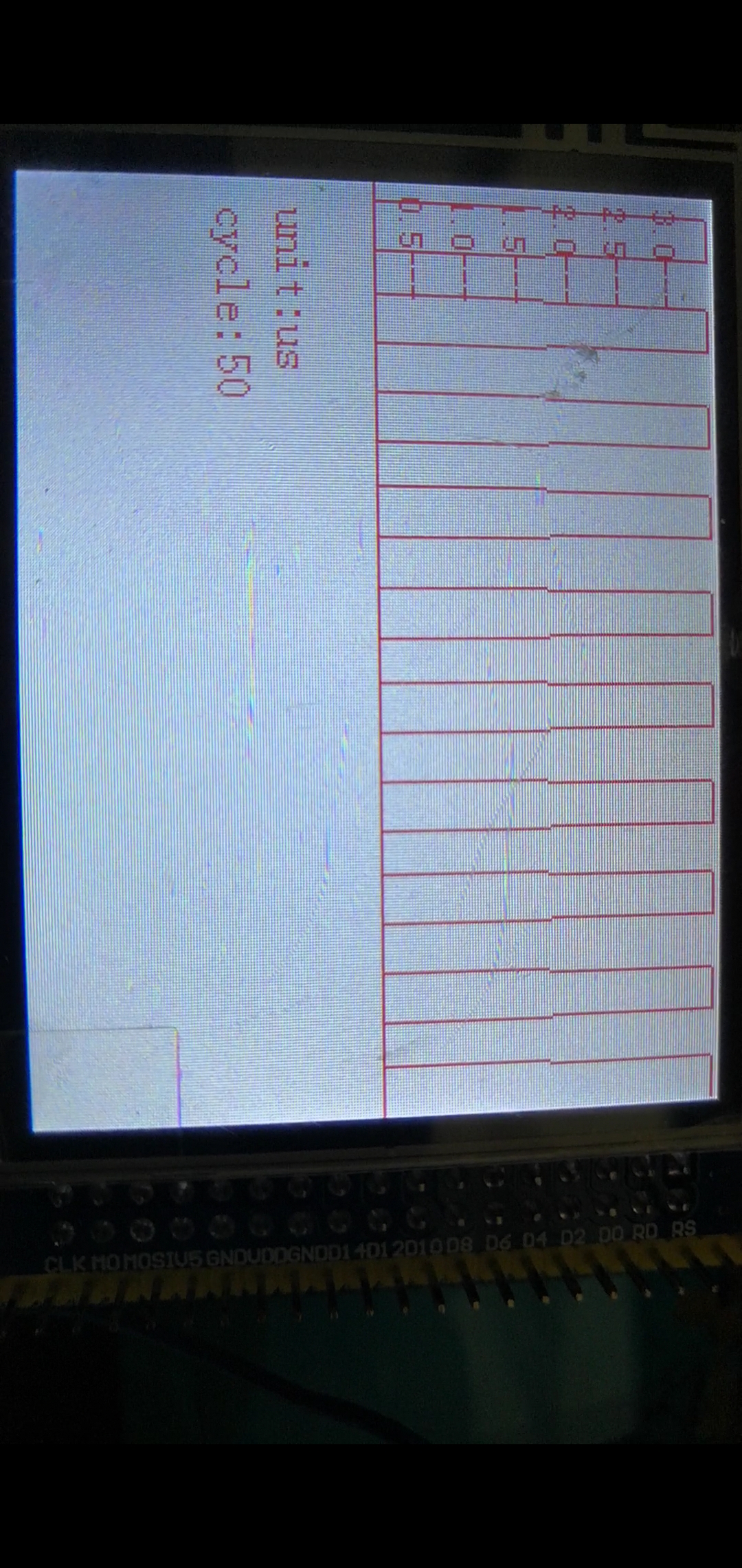
Sine wave (1K)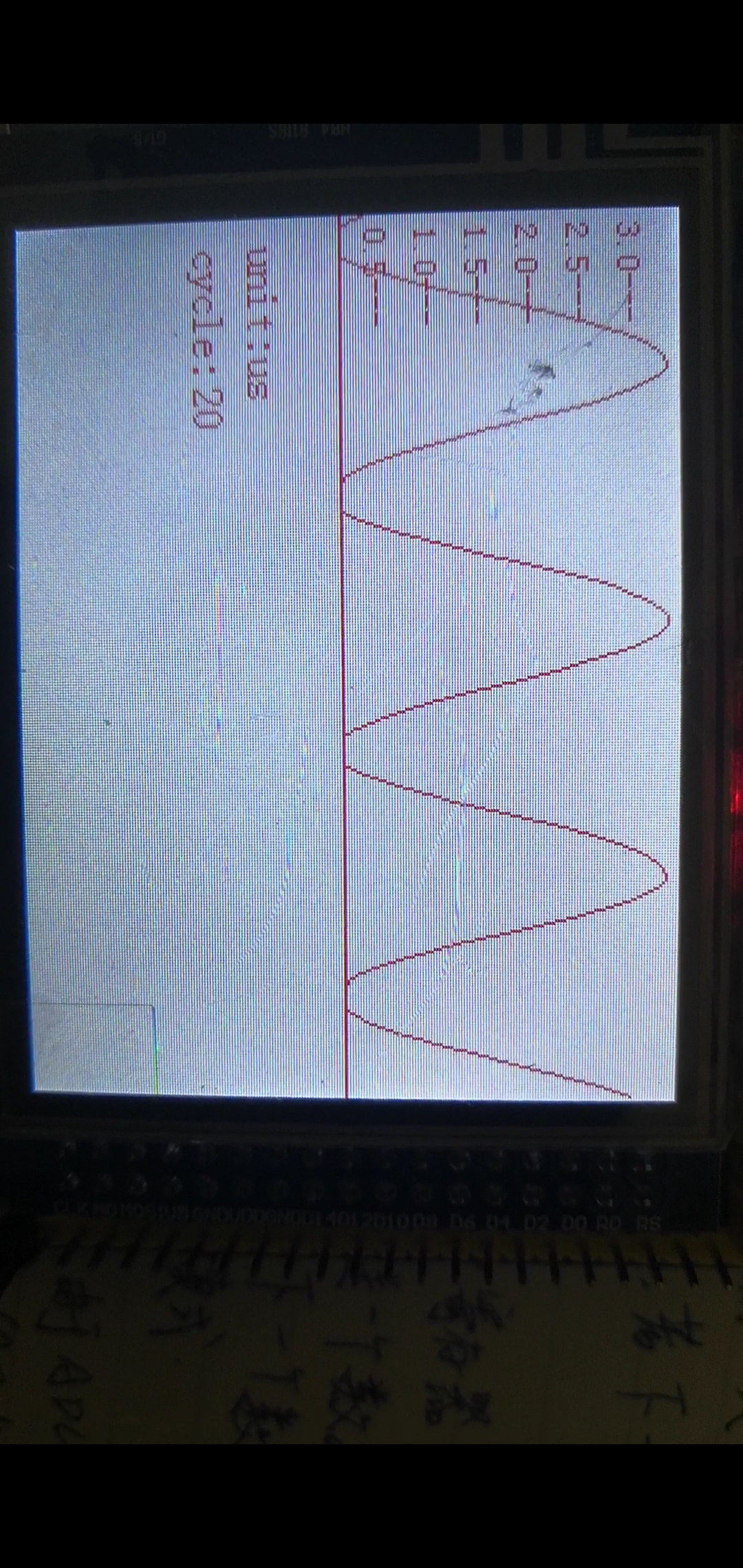
5, Code link
Link: https://pan.baidu.com/s/1-cHCp37KdmSaLiY3-LU4zw
Extraction code: bemx

