1. Introduction to USART
- Universal Synchronous Asynchronous Receiver and Transmitter is a serial communication device that provides flexibility for full duplex data exchange with external devices. Unlike USART, there is also a UART(Universal Asynchronous Receiver and Transmitter), which cuts out the synchronous communication function on the basis of USART and only asynchronous communication. Simple distinction between synchronous and asynchronous means that when communicating, there is no need to provide external clock output. Usually, the serial communication we use is UART.
- Serial communication generally transmits data in frame format, that is, frame by frame, each frame contains start signal, data information, stop information, and possibly check information. USART specifies these transmission parameters, and of course it is not the only parameter value. Many parameter values can be customized, just to enhance its compatibility.
2. Register Address Method
(1) New Keil Project
New Project - > New uVision Project.

Select the storage path, name the file and save it.

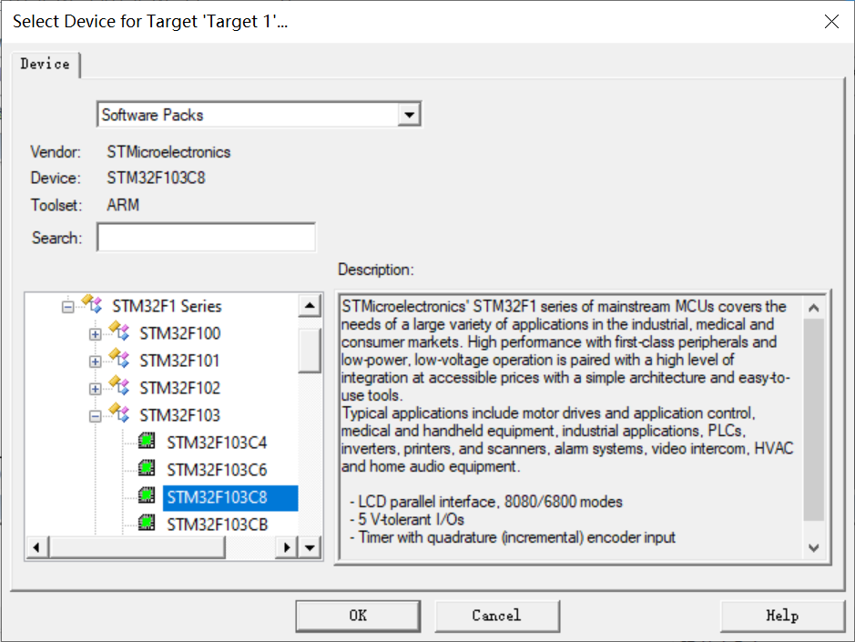
Select the chip and OK.
This step is not selected, click OK.

(2) Write code and compile
Right-click Source Group1 to select ADD New item to Gourp....

Select Asm File (.s) and name it. Click ADD.

hello.s:
;RCC Register Address Image
RCC_BASE            EQU    0x40021000
RCC_CR              EQU    (RCC_BASE + 0x00)
RCC_CFGR            EQU    (RCC_BASE + 0x04)
RCC_CIR             EQU    (RCC_BASE + 0x08)
RCC_APB2RSTR        EQU    (RCC_BASE + 0x0C)
RCC_APB1RSTR        EQU    (RCC_BASE + 0x10)
RCC_AHBENR          EQU    (RCC_BASE + 0x14)
RCC_APB2ENR         EQU    (RCC_BASE + 0x18)
RCC_APB1ENR         EQU    (RCC_BASE + 0x1C)
RCC_BDCR            EQU    (RCC_BASE + 0x20)
RCC_CSR             EQU    (RCC_BASE + 0x24)

;AFIO Register Address Image
AFIO_BASE           EQU    0x40010000
AFIO_EVCR           EQU    (AFIO_BASE + 0x00)
AFIO_MAPR           EQU    (AFIO_BASE + 0x04)
AFIO_EXTICR1        EQU    (AFIO_BASE + 0x08)
AFIO_EXTICR2        EQU    (AFIO_BASE + 0x0C)
AFIO_EXTICR3        EQU    (AFIO_BASE + 0x10)
AFIO_EXTICR4        EQU    (AFIO_BASE + 0x14)

;GPIOA Register Address Image
GPIOA_BASE          EQU    0x40010800
GPIOA_CRL           EQU    (GPIOA_BASE + 0x00)
GPIOA_CRH           EQU    (GPIOA_BASE + 0x04)
GPIOA_IDR           EQU    (GPIOA_BASE + 0x08)
GPIOA_ODR           EQU    (GPIOA_BASE + 0x0C)
GPIOA_BSRR          EQU    (GPIOA_BASE + 0x10)
GPIOA_BRR           EQU    (GPIOA_BASE + 0x14)
GPIOA_LCKR          EQU    (GPIOA_BASE + 0x18)

;GPIO C Port Control
GPIOC_BASE          EQU    0x40011000
GPIOC_CRL           EQU    (GPIOC_BASE + 0x00)
GPIOC_CRH           EQU    (GPIOC_BASE + 0x04)
GPIOC_IDR           EQU    (GPIOC_BASE + 0x08)
GPIOC_ODR           EQU    (GPIOC_BASE + 0x0C)
GPIOC_BSRR          EQU    (GPIOC_BASE + 0x10)
GPIOC_BRR           EQU    (GPIOC_BASE + 0x14)
GPIOC_LCKR          EQU    (GPIOC_BASE + 0x18)

;Serial Port 1 Control
USART1_BASE         EQU    0x40013800
USART1_SR           EQU    (USART1_BASE + 0x00)
USART1_DR           EQU    (USART1_BASE + 0x04)
USART1_BRR          EQU    (USART1_BASE + 0x08)
USART1_CR1          EQU    (USART1_BASE + 0x0c)
USART1_CR2          EQU    (USART1_BASE + 0x10)
USART1_CR3          EQU    (USART1_BASE + 0x14)
USART1_GTPR         EQU    (USART1_BASE + 0x18)

;NVIC Register Address
NVIC_BASE           EQU    0xE000E000
NVIC_SETEN          EQU    (NVIC_BASE + 0x0010)
;SETENA Starting address of register array
NVIC_IRQPRI         EQU    (NVIC_BASE + 0x0400)
;Starting address of interrupt priority register array
NVIC_VECTTBL        EQU    (NVIC_BASE + 0x0D08)
;Address of vector table offset register
NVIC_AIRCR          EQU    (NVIC_BASE + 0x0D0C)
;Address of application interrupt and reset control registers
SETENA0             EQU    0xE000E100
SETENA1             EQU    0xE000E104

;SysTick Register Address
SysTick_BASE        EQU    0xE000E010
SYSTICKCSR          EQU    (SysTick_BASE + 0x00)
SYSTICKRVR          EQU    (SysTick_BASE + 0x04)

;FLASH Buffer Register Address Image
FLASH_ACR           EQU    0x40022000

;SCB_BASE           EQU    (SCS_BASE + 0x0D00)

MSP_TOP             EQU    0x20005000
;Main Stack Start Value
PSP_TOP             EQU    0x20004E00
;Process Stack Start Value

BitAlias_BASE       EQU    0x22000000
;Beginning address of bit band alias area
Flag1               EQU    0x20000200
b_flas              EQU    (BitAlias_BASE + (0x200*32) + (0*4))
;Bit Address
b_05s               EQU    (BitAlias_BASE + (0x200*32) + (1*4))
;Bit Address
DlyI                EQU    0x20000204
DlyJ                EQU    0x20000208
DlyK                EQU    0x2000020C
SysTim              EQU    0x20000210

;Constant Definition
Bit0                EQU    0x00000001
Bit1                EQU    0x00000002
Bit2                EQU    0x00000004
Bit3                EQU    0x00000008
Bit4                EQU    0x00000010
Bit5                EQU    0x00000020
Bit6                EQU    0x00000040
Bit7                EQU    0x00000080
Bit8                EQU    0x00000100
Bit9                EQU    0x00000200
Bit10               EQU    0x00000400
Bit11               EQU    0x00000800
Bit12               EQU    0x00001000
Bit13               EQU    0x00002000
Bit14               EQU    0x00004000
Bit15               EQU    0x00008000
Bit16               EQU    0x00010000
Bit17               EQU    0x00020000
Bit18               EQU    0x00040000
Bit19               EQU    0x00080000
Bit20               EQU    0x00100000
Bit21               EQU    0x00200000
Bit22               EQU    0x00400000
Bit23               EQU    0x00800000
Bit24               EQU    0x01000000
Bit25               EQU    0x02000000
Bit26               EQU    0x04000000
Bit27               EQU    0x08000000
Bit28               EQU    0x10000000
Bit29               EQU    0x20000000
Bit30               EQU    0x40000000
Bit31               EQU    0x80000000

;Vector table
    AREA RESET, DATA, READONLY
    DCD    MSP_TOP            ;Initialize the main stack
    DCD    Start              ;Reset Vector
    DCD    NMI_Handler        ;NMI Handler
    DCD    HardFault_Handler  ;Hard Fault Handler
    DCD    0
    DCD    0
    DCD    0
    DCD    0
    DCD    0
    DCD    0
    DCD    0
    DCD    0
    DCD    0
    DCD    0
    DCD    0
    DCD    SysTick_Handler    ;SysTick Handler
    SPACE  20                 ;Reserved space 20 bytes

;Code snippet
    AREA |.text|, CODE, READONLY
    ;Main program start
    ENTRY
    ;Indicates that the program starts here
Start
    ;Clock System Settings
    ldr    r0, =RCC_CR
    ldr    r1, [r0]
    orr    r1, #Bit16
    str    r1, [r0]
    ;Open external crystal vibration enable
    ;Start External 8 M Crystal oscillator

ClkOk
    ldr    r1, [r0]
    ands   r1, #Bit17
    beq    ClkOk
    ;Waiting for external crystal vibration to be ready
    ldr    r1,[r0]
    orr    r1,#Bit17
    str    r1,[r0]
    ;FLASH Buffer
    ldr    r0, =FLASH_ACR
    mov    r1, #0x00000032
    str    r1, [r0]

    ;Set up PLL Phase-locked loop multiplier is 7,HSE Input nonfrequency Division
    ldr    r0, =RCC_CFGR
    ldr    r1, [r0]
    orr    r1, #(Bit18 :OR: Bit19 :OR: Bit20 :OR: Bit16 :OR: Bit14)
    orr    r1, #Bit10
    str    r1, [r0]
    ;start-up PLL Phase-locked loop
    ldr    r0, =RCC_CR
    ldr    r1, [r0]
    orr    r1, #Bit24
    str    r1, [r0]
PllOk
    ldr    r1, [r0]
    ands   r1, #Bit25
    beq    PllOk
    ;Choice PLL Clock as system clock
    ldr    r0, =RCC_CFGR
    ldr    r1, [r0]
    orr    r1, #(Bit18 :OR: Bit19 :OR: Bit20 :OR: Bit16 :OR: Bit14)
    orr    r1, #Bit10
    orr    r1, #Bit1
    str    r1, [r0]
    ;Other RCC Related Settings
    ldr    r0, =RCC_APB2ENR
    mov    r1, #(Bit14 :OR: Bit4 :OR: Bit2)
    str    r1, [r0]

    ;IO port settings
    ldr    r0, =GPIOC_CRL
    ldr    r1, [r0]
    orr    r1, #(Bit28 :OR: Bit29)
    ;PC.7 Output mode,Maximum Speed 50 MHz
    and    r1, #(~Bit30 & ~Bit31)
    ;PC.7 Universal Push-Pull Output Mode
    str    r1, [r0]

    ;PA9 Serial 0 Launch Foot
    ldr    r0, =GPIOA_CRH
    ldr    r1, [r0]
    orr    r1, #(Bit4 :OR: Bit5)
    ;PA.9 Output mode,Maximum Speed 50 MHz
    orr    r1, #Bit7
    and    r1, #~Bit6
    ;10: Push-Pull Output Mode with Reuse Function
    str    r1, [r0]

    ldr    r0, =USART1_BRR
    mov    r1, #0x271
    str    r1, [r0]
    ;Configure baud rate-> 115200

    ldr    r0, =USART1_CR1
    mov    r1, #0x200c
    str    r1, [r0]
    ;USART Module Always Enable Send and Receive Enables
    ;71 02 00 00   2c 20 00 00

    ;AFIO Parameter Settings
    ;Systick Parameter Settings
    ldr    r0, =SYSTICKRVR
    ;Systick Loading Initial Value
    mov    r1, #9000
    str    r1, [r0]
    ldr    r0, =SYSTICKCSR
    ;Set up,start-up Systick
    mov    r1, #0x03
    str    r1, [r0]

    ;NVIC
    ;ldr   r0, =SETENA0
    ;mov   r1, 0x00800000
    ;str   r1, [r0]
    ;ldr   r0, =SETENA1
    ;mov   r1, #0x00000100
    ;str   r1, [r0]

    ;Switch to user-level threading mode
    ldr    r0, =PSP_TOP
    ;Initialize Thread Stack
    msr    psp, r0
    mov    r0, #3
    msr    control, r0

    ;Initialization SRAM register
    mov    r1, #0
    ldr    r0, =Flag1
    str    r1, [r0]
    ldr    r0, =DlyI
    str    r1, [r0]
    ldr    r0, =DlyJ
    str    r1, [r0]
    ldr    r0, =DlyK
    str    r1, [r0]
    ldr    r0, =SysTim
    str    r1, [r0]

;Main cycle
main
    ldr    r0, =Flag1
    ldr    r1, [r0]
    tst    r1, #Bit1
    ;SysTick Generate 0.5s,Location bit 1
    beq    main                  ;0.5s Sign not yet positioned

    ;0.5s Flag already in place
    ldr    r0, =b_05s
    ;Bit-band operation zeroing 0.5s sign
    mov    r1, #0
    str    r1, [r0]
    bl     LedFlas
    mov    r0, #'H'
    bl     send_a_char
	mov    r0, #'e'
    bl     send_a_char
	mov    r0, #'l'
    bl     send_a_char
	mov    r0, #'l'
    bl     send_a_char
	mov    r0, #'o'
    bl     send_a_char
	mov    r0, #' '
    bl     send_a_char
	mov    r0, #'w'
    bl     send_a_char
	mov    r0, #'o'
    bl     send_a_char
	mov    r0, #'r'
    bl     send_a_char
	mov    r0, #'l'
    bl     send_a_char
	mov    r0, #'d'
    bl     send_a_char
	mov    r0, #'\n'
    bl     send_a_char
	b      main

;Subprogram serial port 1 sends a character
send_a_char
    push   {r0 - r3}
    ldr    r2, =USART1_DR
    str    r0, [r2]
b1
    ldr    r2, =USART1_SR
    ldr    r2, [r2]
    tst    r2, #0x40
    beq    b1
    ;Send complete(Transmission complete)wait for
    pop    {r0 - r3}
    bx     lr

;subroutine led Twinkle
LedFlas
    push   {r0 - r3}
    ldr    r0, =Flag1
    ldr    r1, [r0]
    tst    r1, #Bit0
    ;bit0 Flashing Mark Bit
    beq    ONLED        ;Open for 0 led lamp
    ;Close for 1 led lamp
    ldr    r0, =b_flas
    mov    r1, #0
    str    r1, [r0]
    ;Flash flag position is 0,Next state is on light
    ;PC.7 Output 0
    ldr    r0, =GPIOC_BRR
    ldr    r1, [r0]
    orr    r1, #Bit7
    str    r1, [r0]
    b      LedEx
ONLED
    ;Open for 0 led lamp
    ldr    r0, =b_flas
    mov    r1, #1
    str    r1, [r0]
    ;Flash flag position 1,Next state is off light
    ;PC.7 Output 1
    ldr    r0, =GPIOC_BSRR
    ldr    r1, [r0]
    orr    r1, #Bit7
    str    r1, [r0]
LedEx
    pop    {r0 - r3}
    bx     lr

;Exception Program
NMI_Handler
    bx     lr

HardFault_Handler
    bx     lr

SysTick_Handler
    ldr    r0, =SysTim
    ldr    r1, [r0]
    add    r1, #1
    str    r1, [r0]
    cmp    r1, #500
    bcc    TickExit
    mov    r1, #0
    str    r1, [r0]
    ldr    r0, =b_05s
    ;Clock tick counter settings greater than or equal to 500 zeroes 0.5s Sign bits
    ;Bit band operation position 1
    mov    r1, #1
    str    r1, [r0]
TickExit
    bx     lr

    ALIGN
    ;By using zero or empty instructions NOP Fill,To align the current position with a specified boundary
    END
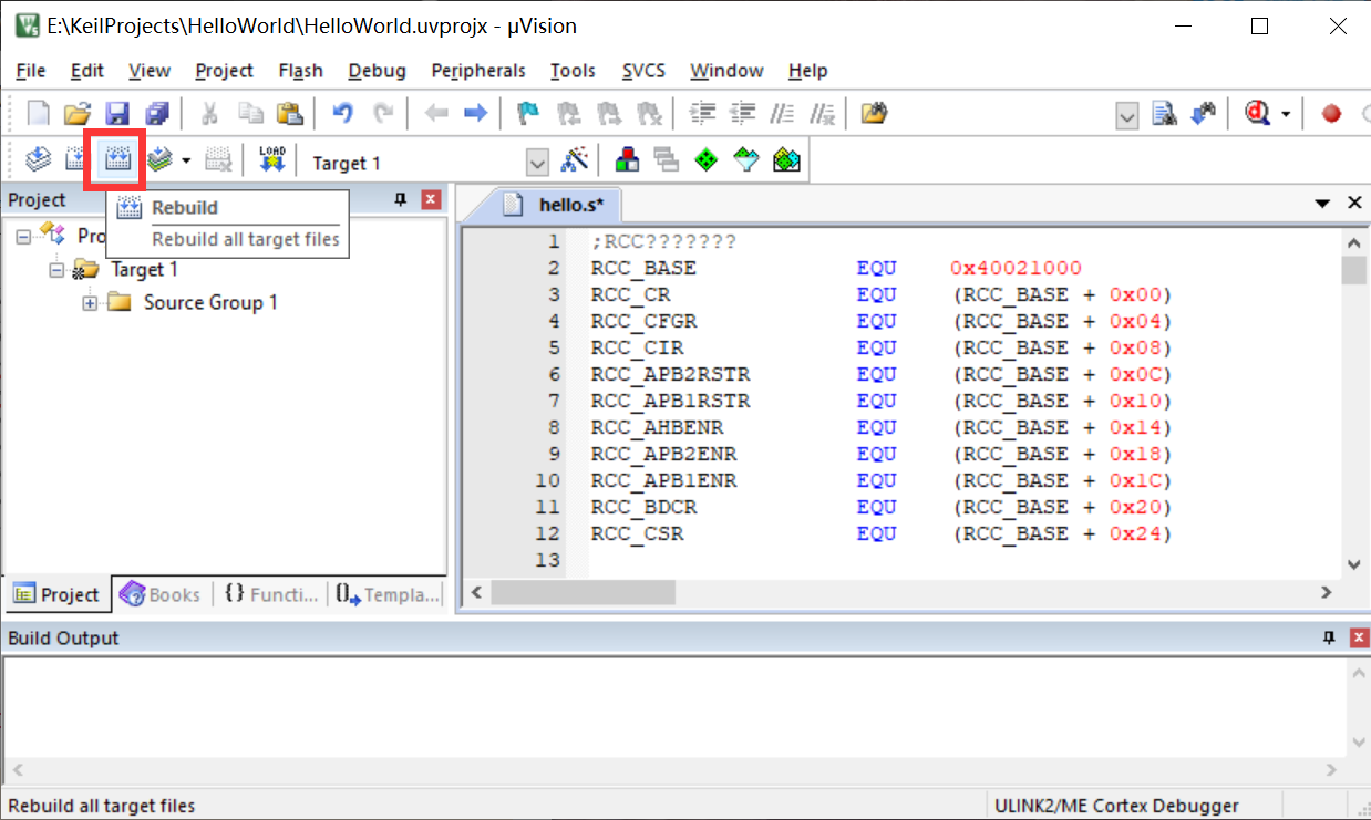
Click on the magic wand, as checked in the figure, to generate the hex file.

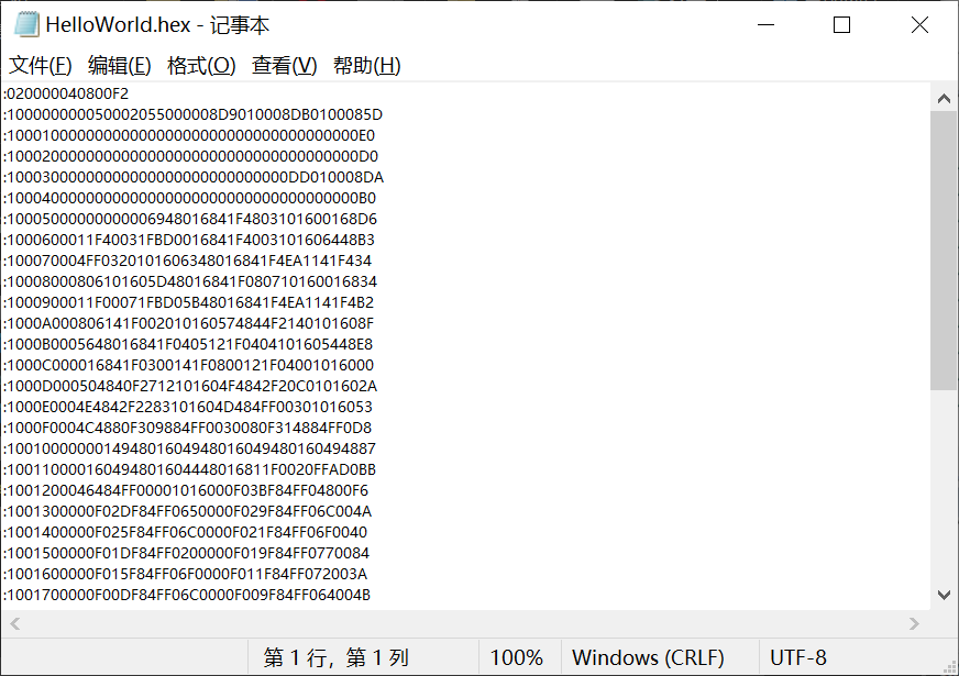
Compile to generate the hex file.

(3) Burning
Connect circuit.
Connect Serial Port
TXD-A10
RXD-A9
3V3-3V3
GND-G
boot0 at 1 and boot1 at 0 during burning
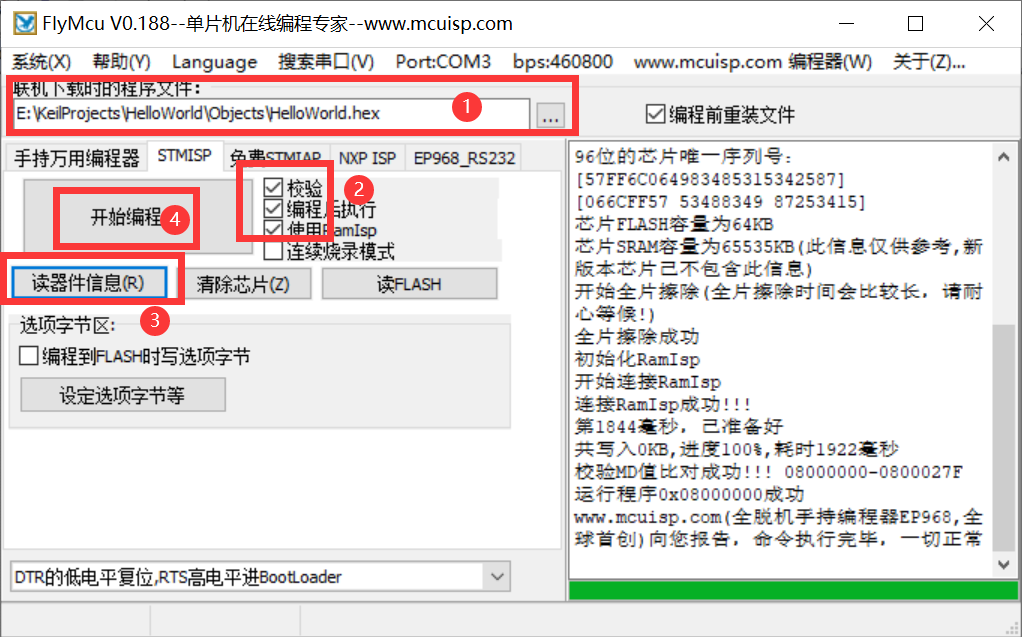
Burning, using either FlyMcu or Mcuisp, was successful as shown in the figure.
(4) Serial output results
At this point boot0 is set at 0, boot1 at 1
Circuit diagram:
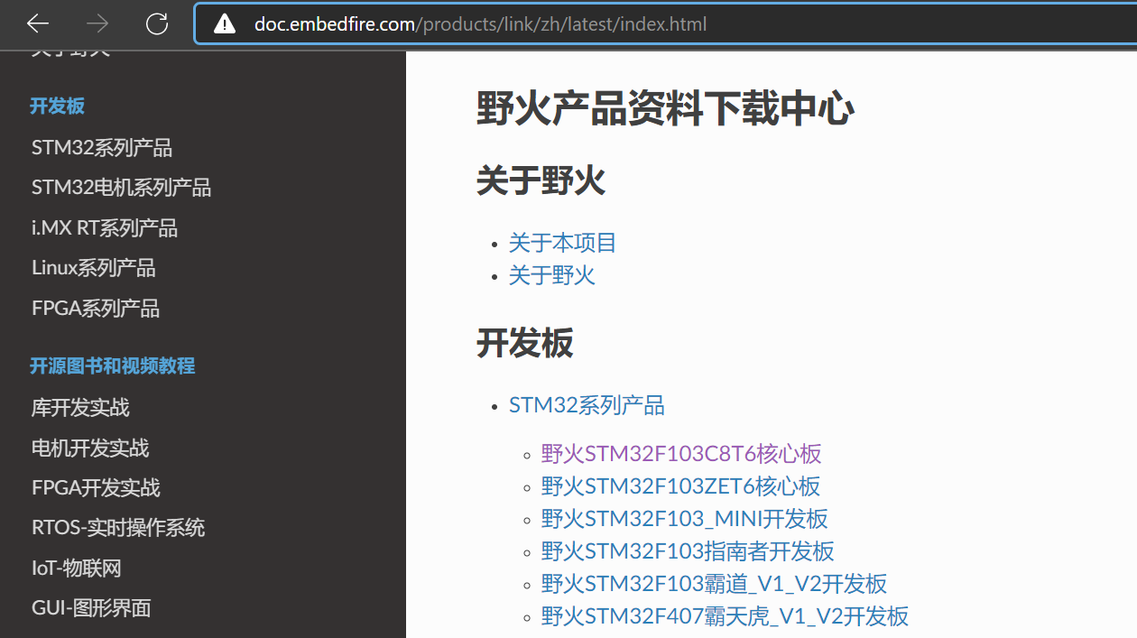
go Wildfire Product Data Download Center Download the STM32F103C8T6 core board, which contains relevant information.
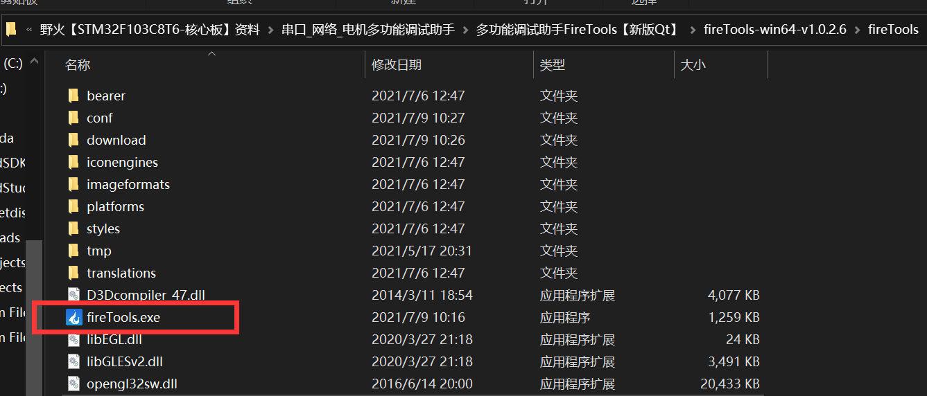
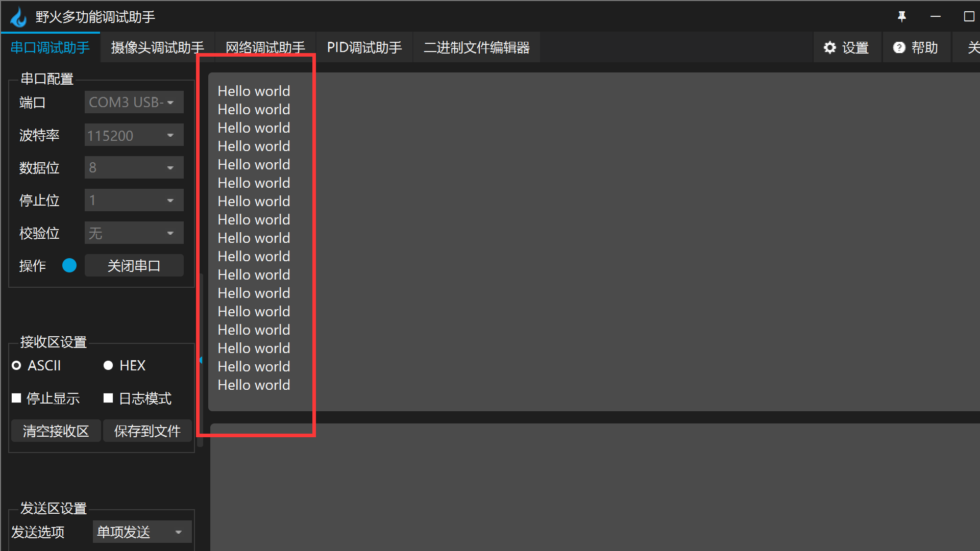
Debug with wildfire multi-function debugging assistant.
Open the serial port.

Output results.
3. HAL Library Mode
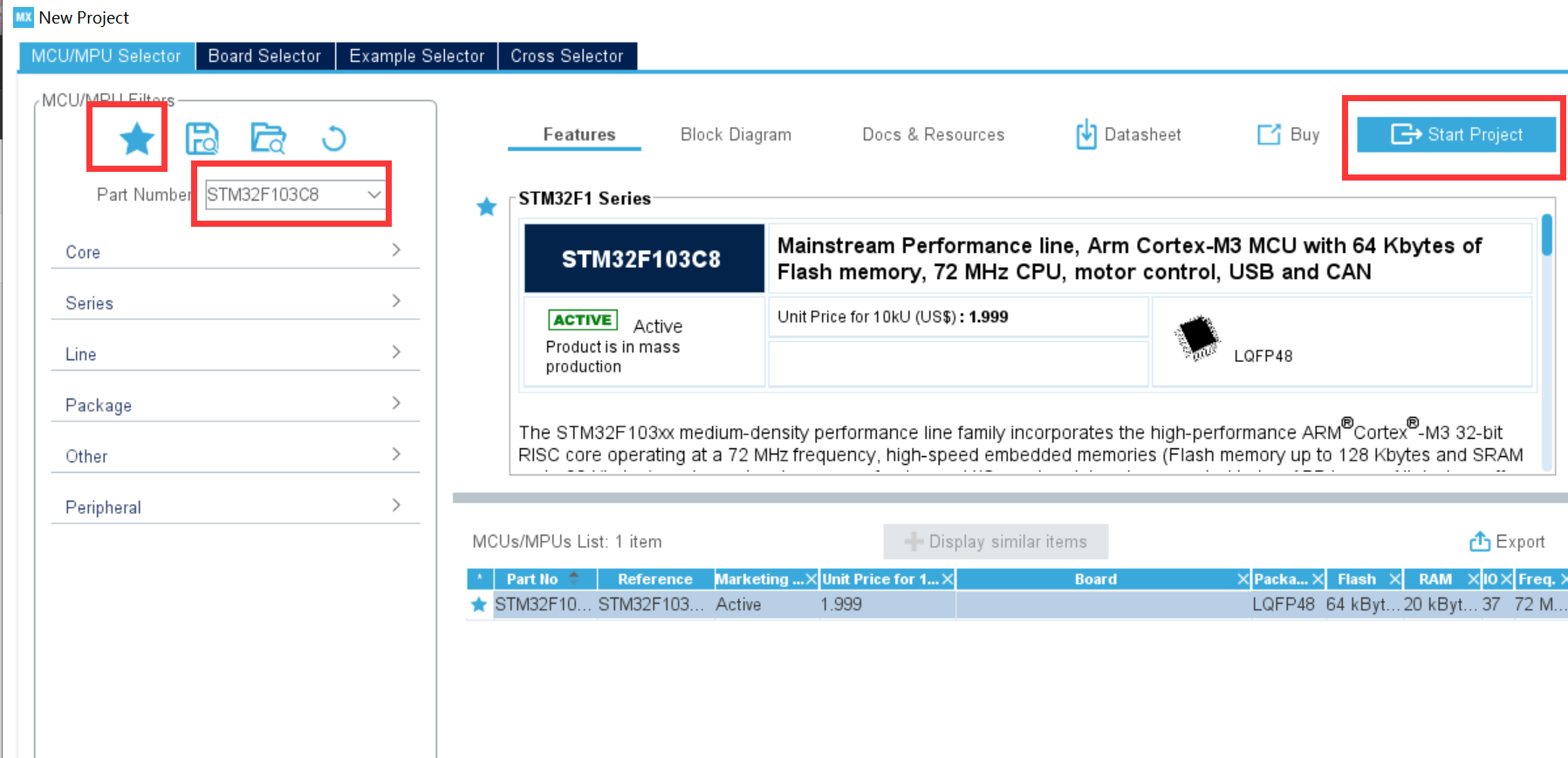
(1) CubeMX Creation Project
New File->New Project.

Choose chip, dot star ⭐, Then Start Project on the right.
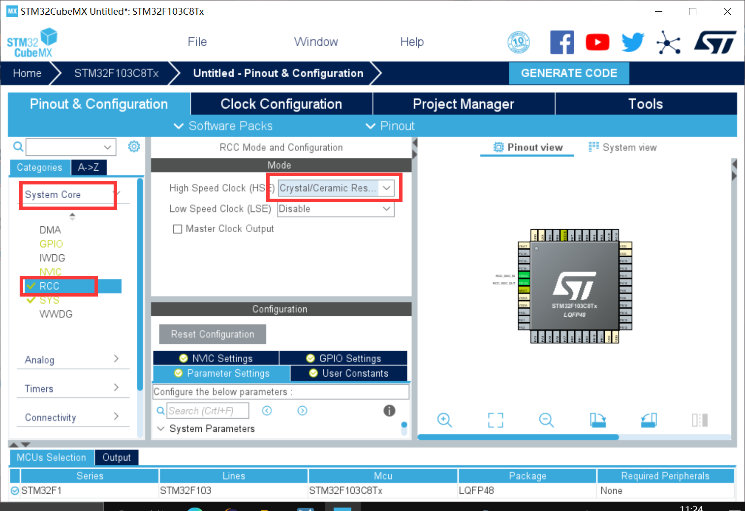
Rcc clock configuration, click System Core, click RCC, and select Crystal/Ceramic Resonator in the HSE option.
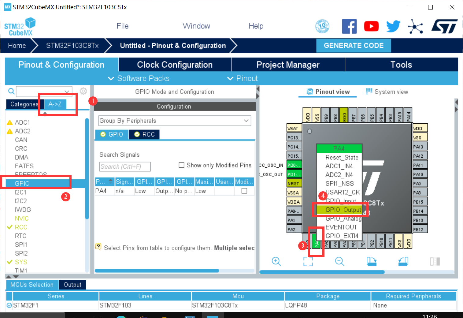
Pin A4.
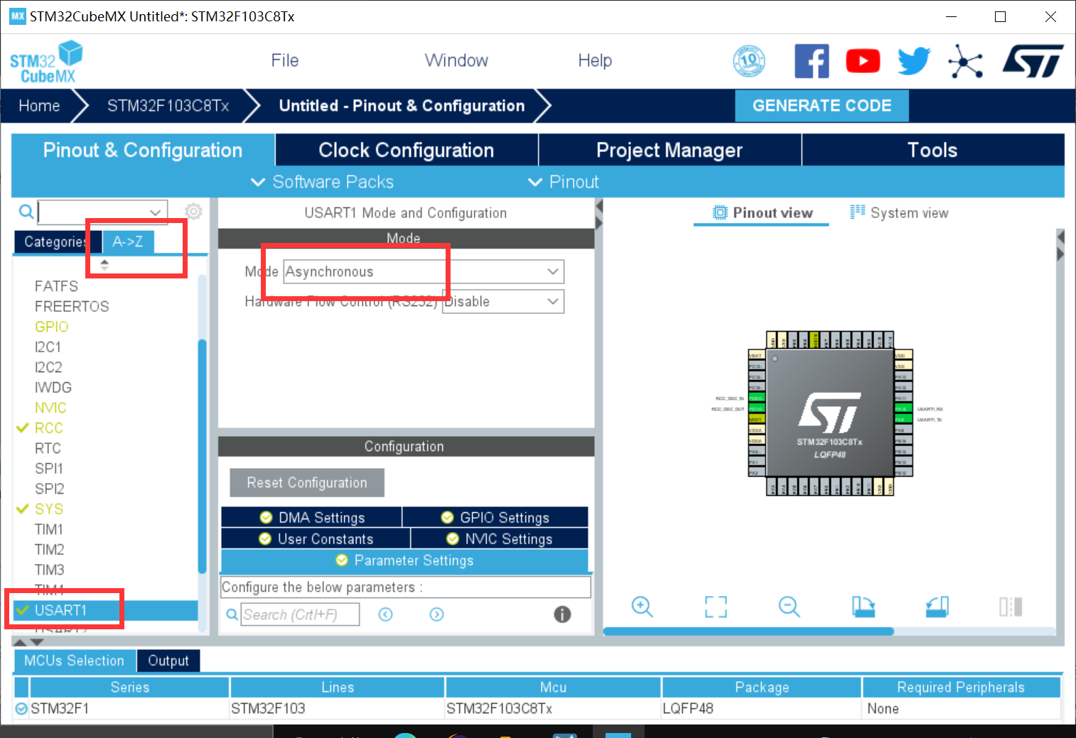
Set USART1.
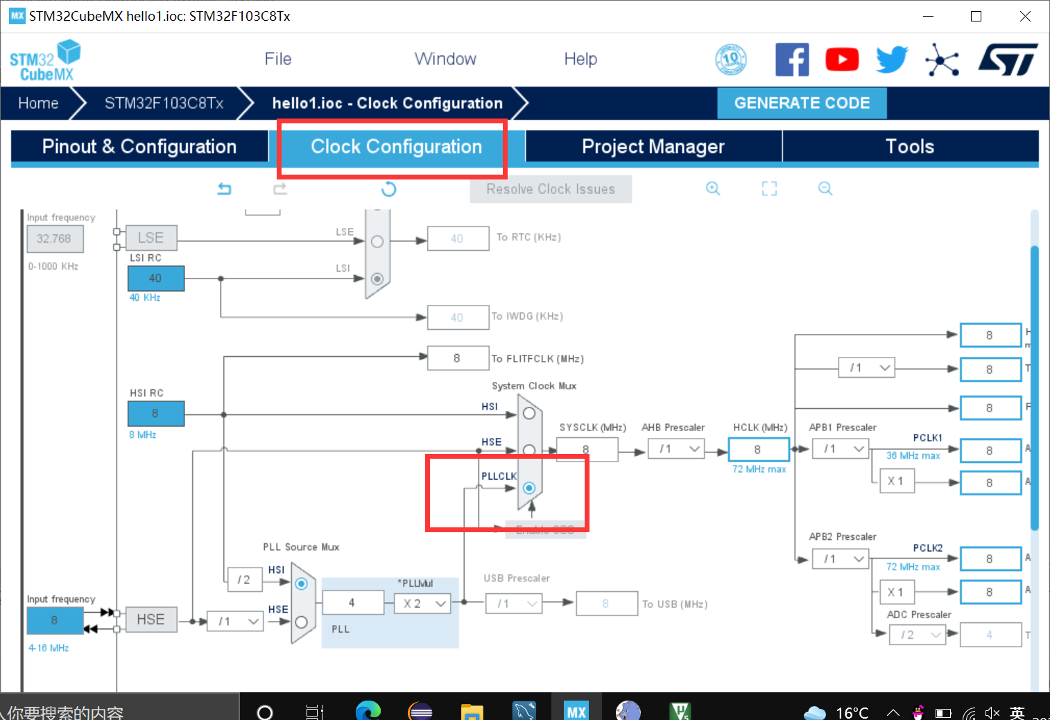
Click Clock Configuration and select PLLCLK.
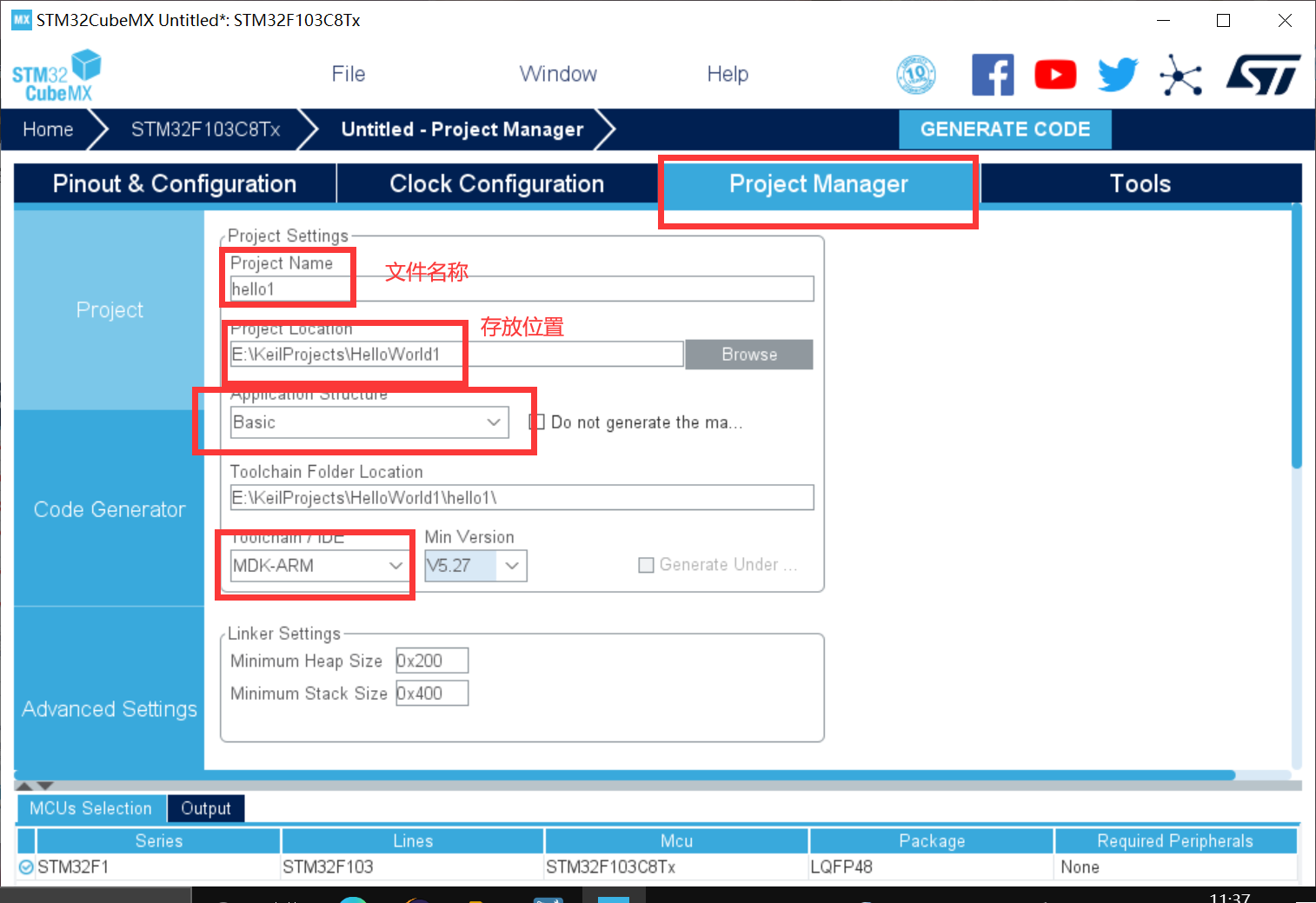
Click project manager to fill in the path and project name.
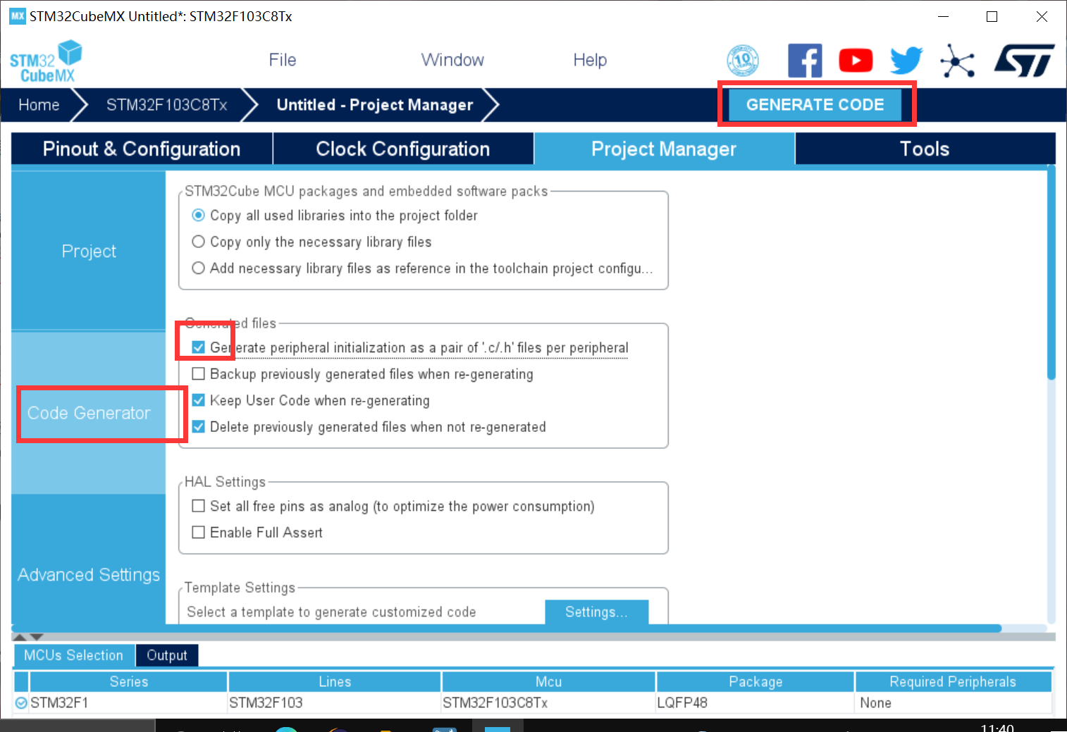
Enter the code generation interface, select Generate initialization.c/.h file, click generate code, and wait.
Click Open to open from Keil.

(2) main.c code modification
After opening with Keil, click on the main.c file to find the while function to add code to it to implement the function.
 char data[]="hello windows!\n";
		HAL_UART_Transmit(&huart1, (uint8_t *)data, 15, 0xffff);
		HAL_Delay(1000);

Compile.
(3) Burning
boot0 at 1, boot1 at 0

(4) Serial output results
Boot0 at 0,Boot1 at 1
Debug with wildfire multi-function debugging assistant, open the serial port, and output successfully.

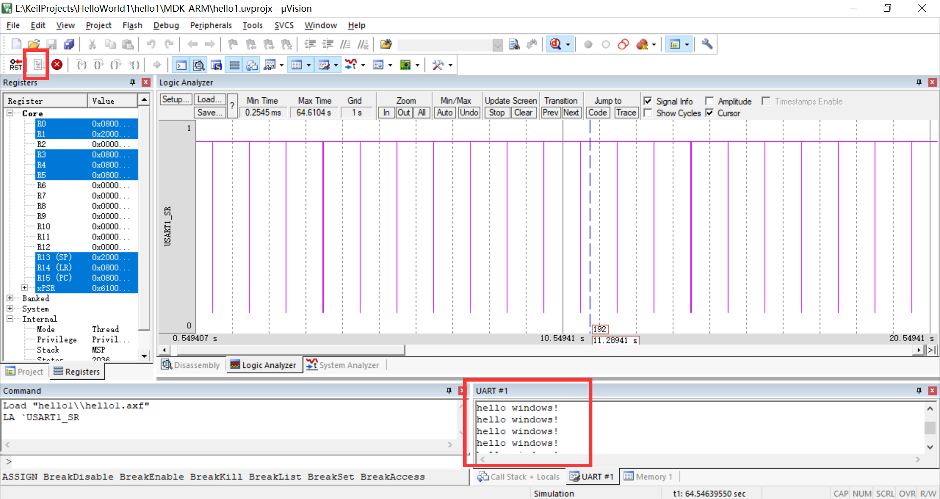
(5) Analyzing waveforms
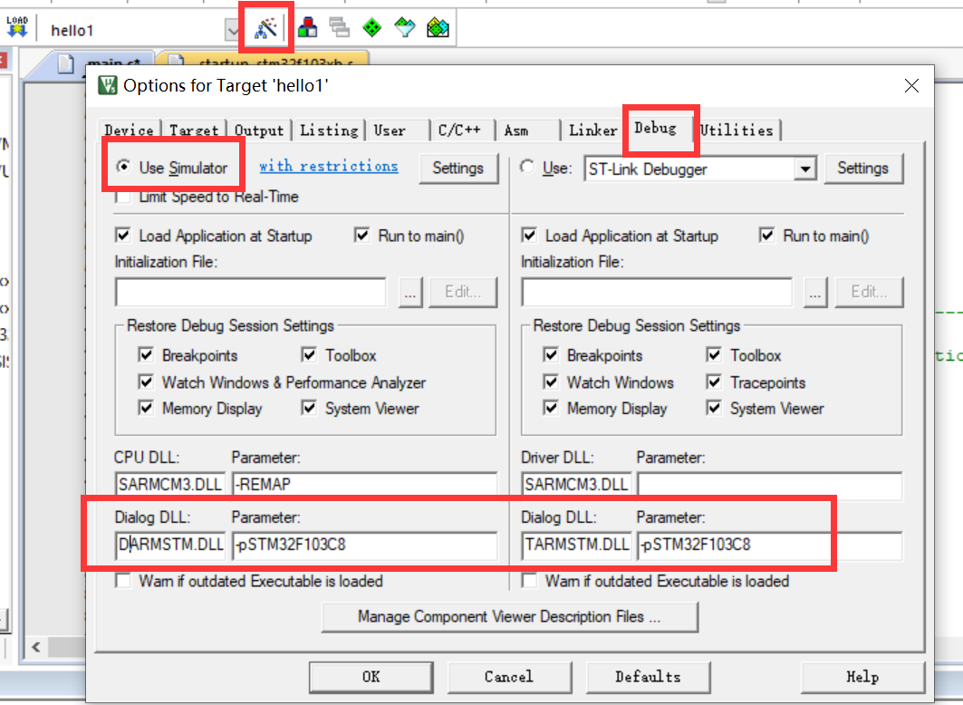
Click on the magic wand to set Debug.
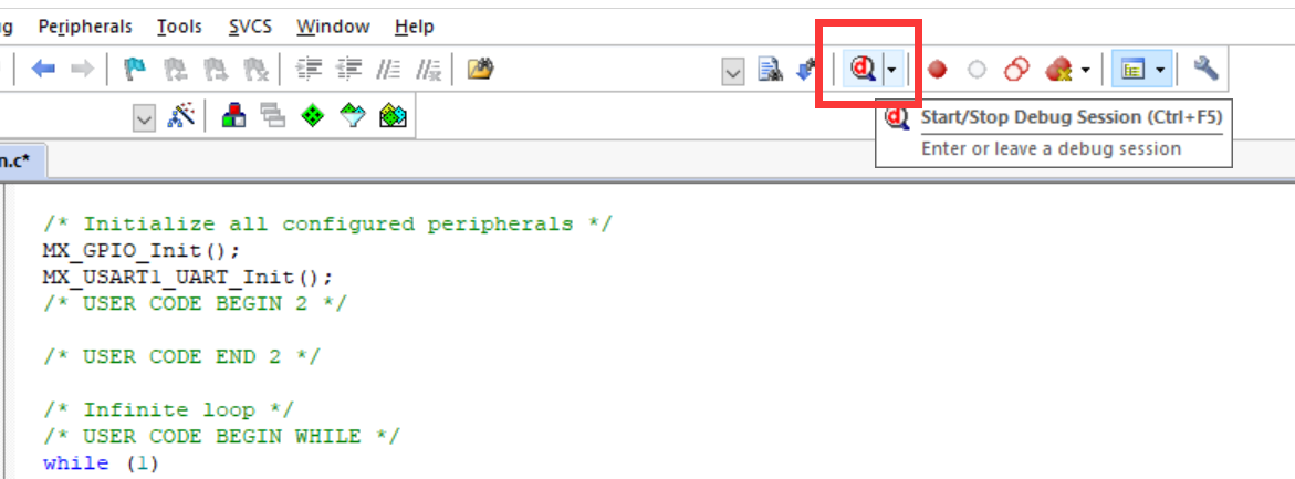
Debugging.
Select a logical analyzer.
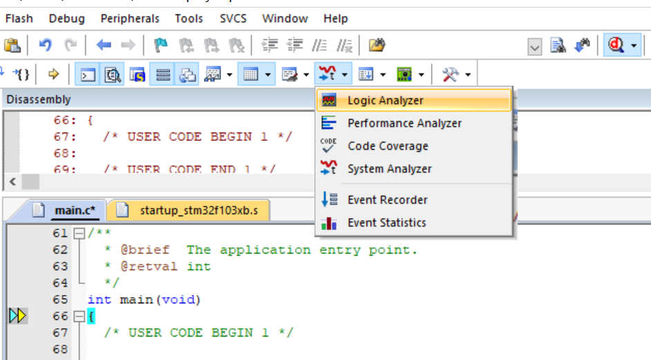
Click Setup.

Run once, output the result.
Reference
STM32 Minimum Core Board F103 Serial Communication USART
STM32 Serial Communication Output Hello Window
STM32 Assembler - Serial Output Hello world