STM32 SPI communication
- High speed full duplex communication bus
SPI communication uses three buses and chip select lines, the three buses are SCK, MOSI and MISO respectively, and the chip select line is NSS(CS)
-
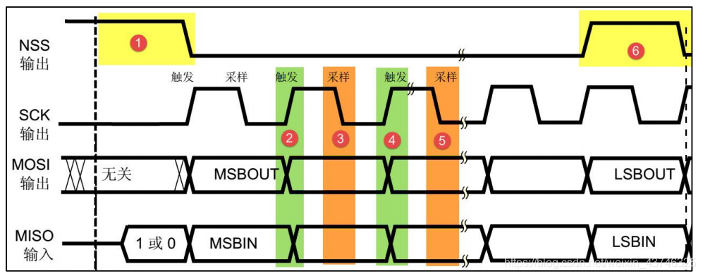
NSS signal line changes from high to low, which is the starting signal of SPI communication. NSS is the exclusive signal line of each slave. When the slave detects the start signal on its own NSS line, it knows that it has been selected by the host and begins to prepare to communicate with the host. At the label in the figure, the NSS signal changes from low to high, which is the stop signal of SPI communication, indicating that this communication is over and the selected state of the slave is cancelled.
-
SPI uses MOSI and MISO signal lines to transmit data, and SCK signal lines to synchronize data. MOSI and MISO data lines transmit one bit of data in each clock cycle of SCK, and the data input and output are carried out at the same time.
-
SPI has four communication modes. Their main differences are the clock state of SCK and data sampling time when the bus is idle. For convenience of explanation, the concepts of "clock polarity CPOL" and "clock phase CPHA" are introduced here.
-
Clock polarity CPOL refers to the level signal of SCK signal line when SPI communication equipment is in idle state (that is, before SPI communication, NSS line is in high level SCK state). When CPOL=0, SCK is low in idle state, and when CPOL=1, it is the opposite.
-
Clock phase CPHA refers to the time of data sampling. When CPHA=0, the signal on MOSI or MISO data line will be sampled at the "odd edge" of SCK clock line. When CPHA=1, the data line is sampled at the "even edge" of SCK.
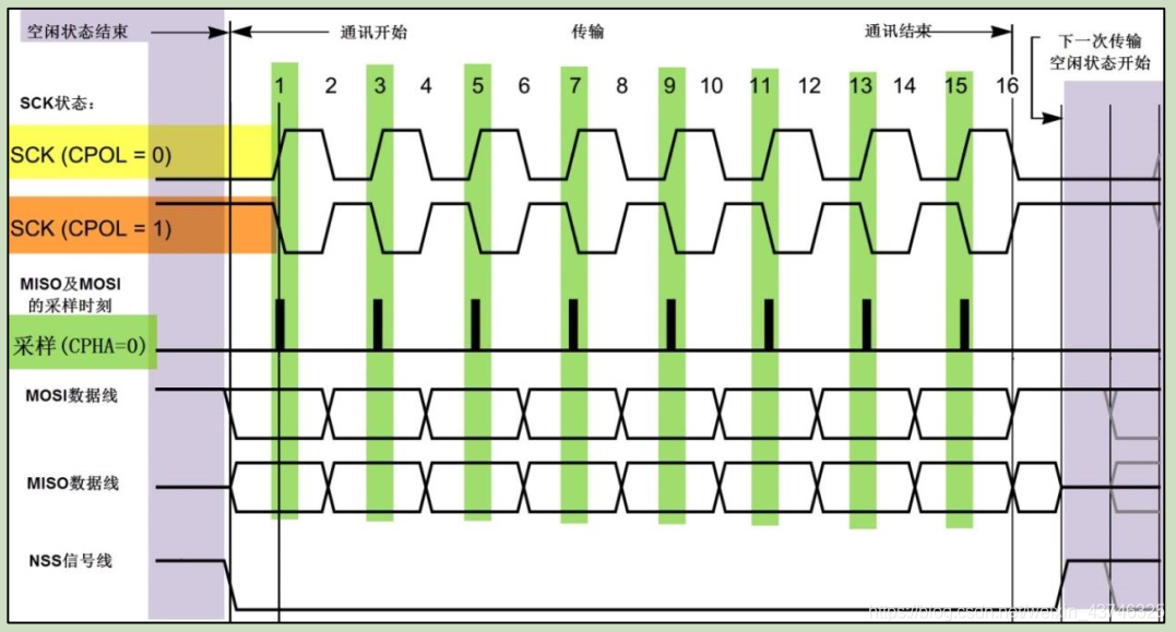
SPI communication mode when CPHA=0
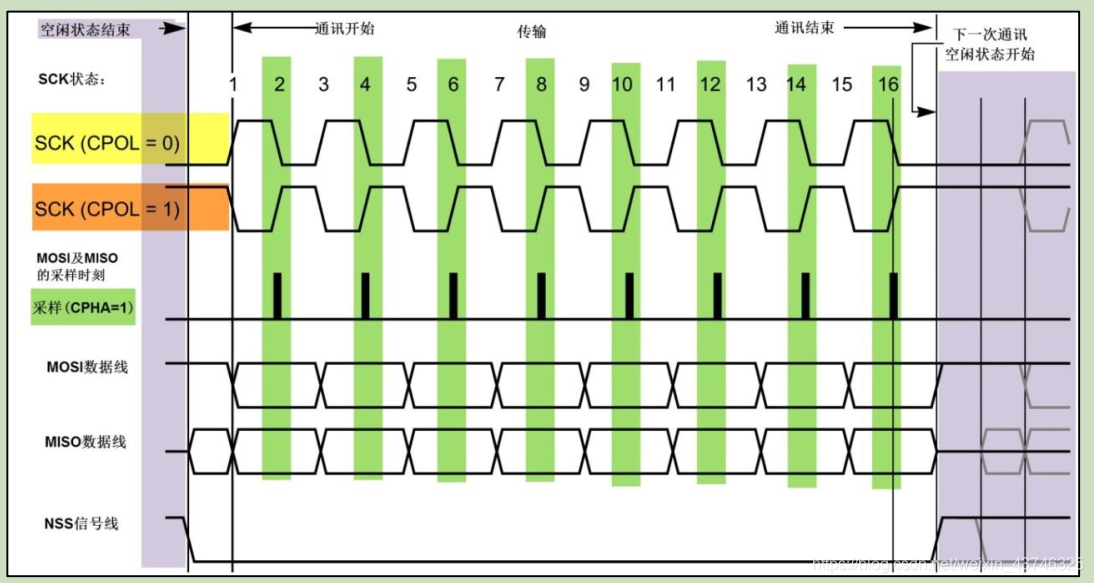
SPI communication mode when CPHA=1:
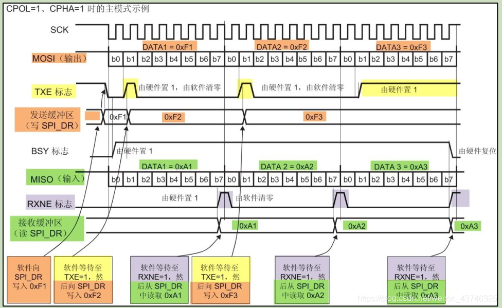
1. First pull down the NSS of the film selection line,
2. Write the data into the transmission buffer, the SCK clock starts to run, and the MOSI will automatically send the data in the transmission buffer. After each frame of data is sent, when the transmission buffer is empty, the TXE flag bit will change to 1 before continuing to send data.
3. Read the data of the reception buffer by judging whether the flag bit of the reception buffer is 1 (the reception buffer is not empty).
-
SCLK signal line is only controlled by master equipment, and slave equipment cannot control signal line. Similarly, in an SPI based device, there is at least one master device;
-
In point-to-point communication, SPI interface does not need addressing operation, and it is full duplex communication, which is simple and efficient. In a system with multiple slaves, each slave needs an independent enable signal, which is slightly more complex in hardware than I2C system.
MSB first (high data first) or LSB first (low data first)?
From the bit point of view, MSB in SPI protocol means to send with high bit first. Similarly, LSB means to send first with low bits. It cannot be confused with the size end.
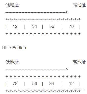
Large end and small end problems (from the perspective of bytes)
big endian means that the low address stores the most significant byte (the high-order byte at the large end is placed at the low address), while little endian means that the low address stores the least significant byte (the low-order byte at the small end is placed at the low address).
For example, taking 0x12345678 as an example, the storage order in two different byte order CPU s
SPI_DEMO practice
STM32 master slave SPI communication test:
Implementation function: the master and slave devices can receive each other's data
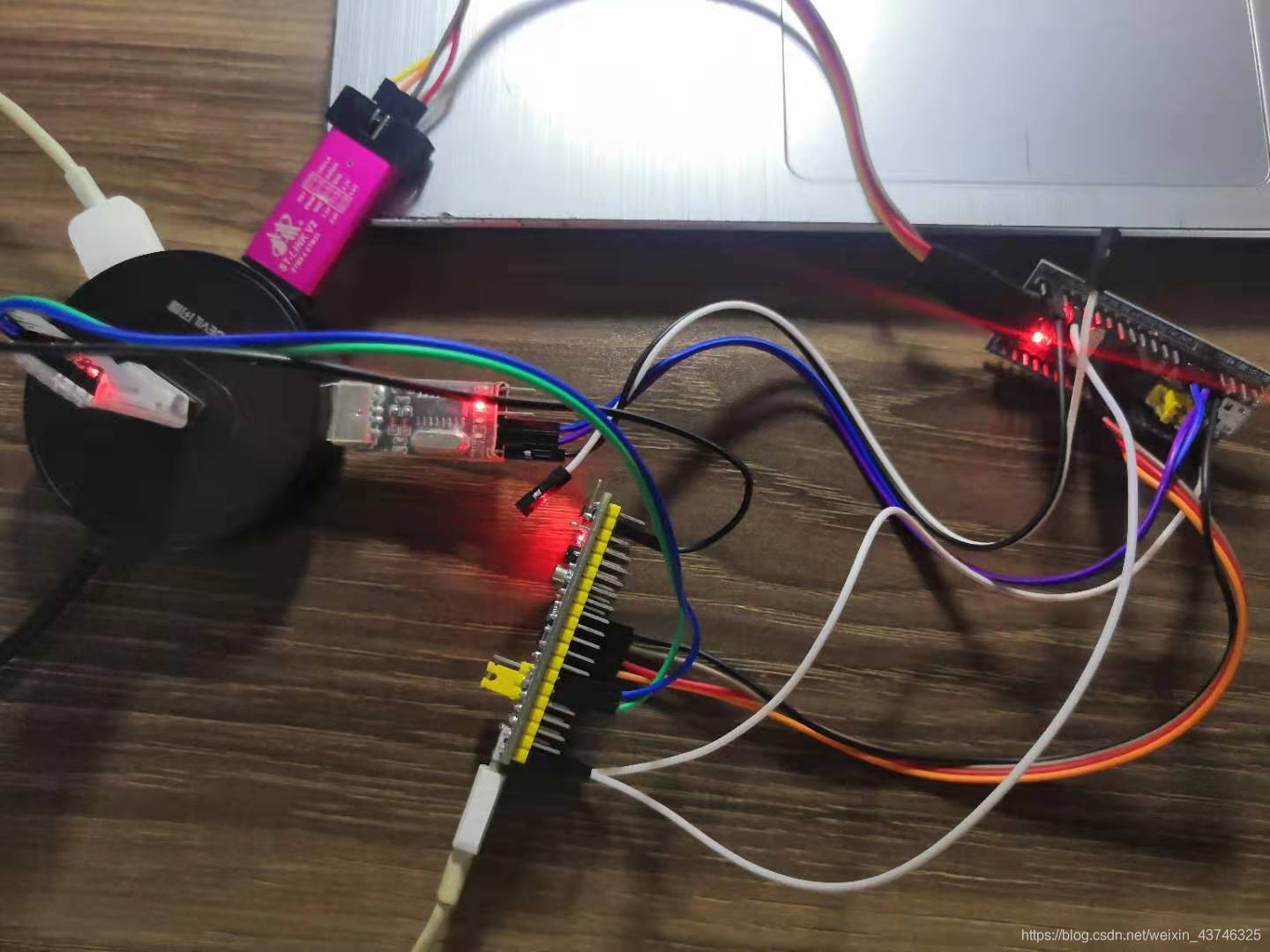
**stm32f103c8t6 main< --—>stm32f103c8t6 from**
Wiring:
| Main (SPI1) | From (SPI1) |
|---|---|
| MOSI(PA7) | MOSI(PA7) |
| MISO(PA6) | MISO(PA6) |
| SPI_CLK(PA5) | SPI_CLK(PA5) |
| SPI_NSS(PA8) | SPI_NSS(PA4) |
The connection is one-to-one. MOSI cannot be connected to MISO, and the configuration parameters of the two devices, such as rate, phase, polarity, CRC, transmission direction and number of bits, must be the same. Remember that they must be grounded together.
Main equipment code:
/*Main equipment stmf103c8 SPI1 */
 int main(void)
 {
   u16 t;
  u8 send_data='A';
  u8 led_flag = 0;
  delay_init();         //Delay function initialization
  NVIC_PriorityGroupConfig(NVIC_PriorityGroup_2); //Set NVIC interrupt packet 2: 2-bit preemption priority and 2-bit response priority
  uart_init(115200);   //The serial port is initialized to 115200
   LED_Init();           //LED port initialization
  KEY_Init();          //Key PB9 pull-up detection low level
  spi_M_init();        //SPI1
  SPI_MCU_CS_LOW();    //The start signal low level is selected to communicate with the slave device
   while(1)
  {
    if(KEY0==0)
    {
      delay_ms(5);
      if(KEY0==0){
      /*Check whether the specified SPI flag bit is set or not: there is no data in the send cache empty flag bit*/
      while (SPI_I2S_GetFlagStatus(MCU_SPIx, SPI_I2S_FLAG_TXE) == RESET); //Check whether the specified SPI flag bit is set or not: send cache empty flag bit
      SPI_I2S_SendData(MCU_SPIx, send_data); //Send a data through the peripheral SPIx
      /*Wait for a byte to be received*/
      while (SPI_I2S_GetFlagStatus(MCU_SPIx, SPI_I2S_FLAG_RXNE) == RESET);
      /*Send the data sent by the slave device, that is, the data received by the master device, to the serial port transmission buffer*/
      USART1->DR = SPI_I2S_ReceiveData(MCU_SPIx);
      led_flag++;
      send_data++;}
      while(KEY0==0);
    }else{

    }
    if(led_flag%2)
      GPIO_SetBits(GPIOC,GPIO_Pin_13);
    else
      GPIO_ResetBits(GPIOC,GPIO_Pin_13);
  }
 }

//spi main mode configuration
void spi_M_init(void){
  SPI_InitTypeDef  SPI_InitStructure;
  GPIO_InitTypeDef GPIO_InitStructure;
  NVIC_InitTypeDef NVIC_InitStructure;
  /* Enable SPI clock */
  MCU_SPI_APBxClock_FUN ( MCU_SPI_CLK, ENABLE );

  /* Enables the clock associated with the SPI pin */
   MCU_SPI_CS_APBxClock_FUN ( MCU_SPI_CS_CLK|MCU_SPI_SCK_CLK|MCU_SPI_MISO_PIN|MCU_SPI_MOSI_PIN, ENABLE );
  /* Configure the CS pin of SPI, just ordinary IO */
  GPIO_InitStructure.GPIO_Pin = MCU_SPI_CS_PIN;
  GPIO_InitStructure.GPIO_Speed = GPIO_Speed_50MHz;
  GPIO_InitStructure.GPIO_Mode = GPIO_Mode_Out_PP;
  GPIO_Init(MCU_SPI_CS_PORT, &GPIO_InitStructure);

  /* Configure the SCK pin of SPI*/
  GPIO_InitStructure.GPIO_Pin = MCU_SPI_SCK_PIN;
  GPIO_InitStructure.GPIO_Mode = GPIO_Mode_AF_PP;
  GPIO_Init(MCU_SPI_SCK_PORT, &GPIO_InitStructure);

  /* Configure MISO pin of SPI*/
  GPIO_InitStructure.GPIO_Pin = MCU_SPI_MISO_PIN;
  GPIO_Init(MCU_SPI_MISO_PORT, &GPIO_InitStructure);

  /* Configure the MOSI pin of SPI*/
  GPIO_InitStructure.GPIO_Pin = MCU_SPI_MOSI_PIN;
  GPIO_Init(MCU_SPI_MOSI_PORT, &GPIO_InitStructure);

  /* Stop signal MCU: CS pin high level*/
  SPI_MCU_CS_HIGH();
  /* SPI Mode configuration */
  // MCU chip supports SPI mode 0 and mode 3, and cpol and CPHA are set accordingly
  SPI_InitStructure.SPI_Direction = SPI_Direction_2Lines_FullDuplex;
  SPI_InitStructure.SPI_Mode = SPI_Mode_Master;
  SPI_InitStructure.SPI_DataSize = SPI_DataSize_8b;
  SPI_InitStructure.SPI_CPOL = SPI_CPOL_High;
  SPI_InitStructure.SPI_CPHA = SPI_CPHA_2Edge;
  SPI_InitStructure.SPI_NSS = SPI_NSS_Soft;//Need attention
  SPI_InitStructure.SPI_BaudRatePrescaler = SPI_BaudRatePrescaler_256;//
  SPI_InitStructure.SPI_FirstBit = SPI_FirstBit_MSB;
  SPI_InitStructure.SPI_CRCPolynomial = 7;
  SPI_Init(MCU_SPIx , &SPI_InitStructure);
  /* Enable SPI  */
  SPI_Cmd(MCU_SPIx , ENABLE);

  //SPI_I2S_ITConfig(MCU_SPIx, SPI_I2S_IT_RXNE, ENABLE);  //  Enable receive interrupt
  /* NVIC Interrupt controller configuration */
//  NVIC_PriorityGroupConfig(NVIC_PriorityGroup_2);      //  Interrupt priority group 2

//  NVIC_InitStructure.NVIC_IRQChannel = SPI1_IRQn;      // SPI2 interrupt
//  NVIC_InitStructure.NVIC_IRQChannelPreemptionPriority=1;  //  Preemption priority 3
//  NVIC_InitStructure.NVIC_IRQChannelSubPriority =3;    //  Sub priority 3
//  NVIC_InitStructure.NVIC_IRQChannelCmd = ENABLE;      // IRQ channel enable
//  NVIC_ Init(&NVIC_InitStructure);              //  Initializes the VIC register according to the specified parameters
}
Slave main code:
- In order to enable the host to receive valid data at the beginning, first store the data to be sent to the transmission buffer SPI_I2S_SendData(MCU_SPIx,‘n’);. It should be noted that at this time, the data has not been sent to the master device, because the slave device cannot actively send data, but passively sends data. You have to wait for the master device to send data. To put it bluntly, you have to wait for a cycle of clock signal. The slave device receives the clock signal (CLK), moves the data of the transmission buffer to the shift register and sends it to the master device.
- Because it is a slave device, SPI1 chip selection pin and hardware chip selection will be multiplexed.
//stm32f103c8 slave
 int main(void)
 {
   u16 retry;
  u8 send_data='a';

  u8 led_flag=0;
  delay_init();         //Delay function initialization
  NVIC_PriorityGroupConfig(NVIC_PriorityGroup_2); //Set NVIC interrupt packet 2: 2-bit preemption priority and 2-bit response priority
  uart_init(115200);   //The serial port is initialized to 115200
   LED_Init();           //LED port initialization
   KEY_Init();
  spi_S_init();
  while (SPI_I2S_GetFlagStatus(MCU_SPIx, SPI_I2S_FLAG_TXE) == RESET); //Check whether the specified SPI flag bit is set or not: cache non empty flag bits are accepted
  SPI_I2S_SendData(MCU_SPIx,'n');//

   while(1)
  {
 //   while (SPI_I2S_GetFlagStatus(MCU_SPIx, SPI_I2S_FLAG_TXE) == RESET); // Check whether the specified SPI flag bit is set or not: cache non empty flag bits are accepted
  //  SPI_I2S_SendData(MCU_SPIx,'n');
 }
}
//spi slave mode configuration
void spi_S_init(void){
  SPI_InitTypeDef  SPI_InitStructure;
  GPIO_InitTypeDef GPIO_InitStructure;
  NVIC_InitTypeDef NVIC_InitStructure;
  /* Enable SPI clock */
  MCU_SPI_APBxClock_FUN ( MCU_SPI_CLK, ENABLE );
  /* Enables the clock associated with the SPI pin */
   MCU_SPI_CS_APBxClock_FUN ( MCU_SPI_CS_CLK|MCU_SPI_SCK_CLK|MCU_SPI_MISO_PIN|MCU_SPI_MOSI_PIN, ENABLE );

  /* Configure the CS pin of SPI, just ordinary IO */
  GPIO_InitStructure.GPIO_Pin = MCU_SPI_CS_PIN;
//  GPIO_InitStructure.GPIO_Speed = GPIO_Speed_50MHz;
  GPIO_InitStructure.GPIO_Mode = GPIO_Mode_AF_PP;
  GPIO_Init(MCU_SPI_CS_PORT, &GPIO_InitStructure);

  /* Configure the SCK pin of SPI*/
  GPIO_InitStructure.GPIO_Pin = MCU_SPI_SCK_PIN;
  GPIO_InitStructure.GPIO_Mode = GPIO_Mode_AF_PP;
  GPIO_Init(MCU_SPI_SCK_PORT, &GPIO_InitStructure);

  /* Configure MISO pin of SPI*/
  GPIO_InitStructure.GPIO_Pin = MCU_SPI_MISO_PIN;
  GPIO_Init(MCU_SPI_MISO_PORT, &GPIO_InitStructure);

  /* Configure the MOSI pin of SPI*/
  GPIO_InitStructure.GPIO_Pin = MCU_SPI_MOSI_PIN;
  GPIO_Init(MCU_SPI_MOSI_PORT, &GPIO_InitStructure);

  /* Stop signal MCU: CS pin high level*/
//  SPI_MCU_CS_HIGH();
  /* SPI Mode configuration */
  // MCU chip supports SPI mode 0 and mode 3, and cpol and CPHA are set accordingly
  SPI_InitStructure.SPI_Direction = SPI_Direction_2Lines_FullDuplex;
  SPI_InitStructure.SPI_Mode = SPI_Mode_Slave;
  SPI_InitStructure.SPI_DataSize = SPI_DataSize_8b;
  SPI_InitStructure.SPI_CPOL = SPI_CPOL_High;
  SPI_InitStructure.SPI_CPHA = SPI_CPHA_2Edge;
  SPI_InitStructure.SPI_NSS = SPI_NSS_Hard;//Select as slave
  SPI_InitStructure.SPI_BaudRatePrescaler = SPI_BaudRatePrescaler_256;
  SPI_InitStructure.SPI_FirstBit = SPI_FirstBit_MSB;
  SPI_InitStructure.SPI_CRCPolynomial = 7;
  SPI_Init(MCU_SPIx , &SPI_InitStructure);

  /* Enable SPI  */
  SPI_Cmd(MCU_SPIx , ENABLE);
  SPI_I2S_ITConfig(MCU_SPIx, SPI_I2S_IT_RXNE, ENABLE);  // Enable receive interrupt


  NVIC_InitStructure.NVIC_IRQChannel = SPIX_IRQ;      // SPI1 interrupt
  NVIC_InitStructure.NVIC_IRQChannelPreemptionPriority=1;  // Preemption priority 3
  NVIC_InitStructure.NVIC_IRQChannelSubPriority =3;    // Sub priority 3
  NVIC_InitStructure.NVIC_IRQChannelCmd = ENABLE;      // IRQ channel enable
  NVIC_Init(&NVIC_InitStructure);              // Initializes the VIC register according to the specified parameters
}
u8 send_data='a';
u8 led_flag=0;
//Interrupt handling function
void handle_spi_fun(void)
{

  /* Judge whether the receive buffer is not empty */
  if (SET == SPI_I2S_GetITStatus(MCU_SPIx, SPI_I2S_IT_RXNE))
  {

    USART1->DR = MCU_SPIx->DR;             /* Read receive buffer data */
    while (SPI_I2S_GetFlagStatus(MCU_SPIx, SPI_I2S_FLAG_TXE) == RESET);
    MCU_SPIx->DR = send_data;
    if(led_flag%2)
      GPIO_ResetBits(GPIOC,GPIO_Pin_13);
    else
      GPIO_SetBits(GPIOC,GPIO_Pin_13);
    led_flag++;
    send_data++;
    /* Clear interrupt flag */
    SPI_I2S_ClearITPendingBit(MCU_SPIx, SPI_I2S_IT_RXNE);
  }
}
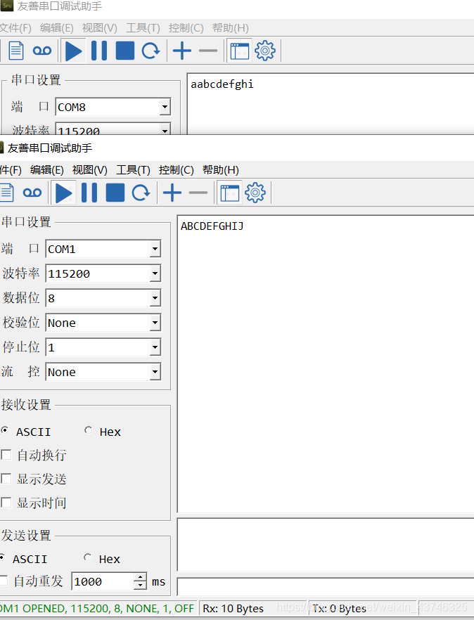
Test effect:
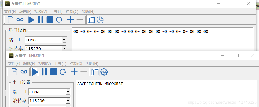 COM8 is the data received by the master device from the slave device, and COM4 is the data received by the slave device from the master device
Obviously, the master device failed to successfully obtain the data from the slave device, and the slave device received the data from the master device.
Problem analysis:
1. The problem occurs in the master device: the master device does not receive or respond.
2. The problem is with the slave device: the slave device does not send data.
3. The above two problems occur at the same time.
Troubleshooting problem:
1. First, I connect the MOSI of the master device to the MISO of my own master device. The test results show that the master device can receive data. The first possibility is ruled out.
2. When the master and slave devices communicate, the logic analyzer is used to detect the MISO pin, and no waveform change can be detected. The problem is probably from the device.
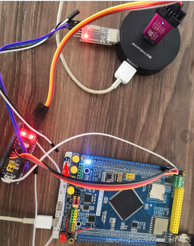
Therefore, I changed the slave device to STM32F429. The master device is still STM32F103C8, and the program is the same.
stm32f103c8t6 main< --—>stm32f429IG from
Wiring:
| Main (SPI1) | From (SPI2) |
|---|---|
| MOSI(PA7) | MOSI(PB15) |
| MISO(PA6) | MISO(PB14) |
| SPI_CLK(PA5) | SPI_CLKP(B13) |
| SPI_NSS(PA8) | SPI_NSS(PB12) |
/*stm32F429IG SPI2 Slave device*/
#define SELECT_MASTER 0
int main(void)
{
u8 send_data='a';
u8 led_flag=0;
LED_GPIO_Config();//PB0 PB1
Debug_USART_Config();//Serial port 1 115200
SPI_MCU_Init();//SPI2
key_init();//PA0 key
#if SELECT_MASTER / / in bsp_spi_mcu.h file settings
send_data='A';
#else
/*Points to pay attention to when judging that the send buffer is empty
As a slave device, the data is put into the send buffer and has not been sent to the master device,
To wait for the master device to send data, that is, a clock signal (SCK) is required
*/
while (SPI_I2S_GetFlagStatus(MCU_SPI, SPI_I2S_FLAG_TXE) == RESET);
/* Write the data register and write the data to be written to the transmission buffer */
SPI_I2S_SendData(MCU_SPI, send_data);
#endif
while(1){
//Main equipment
#if SELECT_MASTER / / in bsp_spi_mcu.h file settings
if(KEY==1)
{
delay(0x0F);
if(KEY==1){
/*Judge that the send buffer is empty and there is no data*/
while (SPI_I2S_GetFlagStatus(MCU_SPI, SPI_I2S_FLAG_TXE) == RESET);
/* Write the data register and write the data to be written to the transmission buffer */
SPI_I2S_SendData(MCU_SPI, send_data);
/*Judge that the receiving buffer is non empty data*/
while (SPI_I2S_GetFlagStatus(MCU_SPI, SPI_I2S_FLAG_RXNE) == RESET);
/*Send the received data to the serial port send buffer*/
USART1->DR = SPI_I2S_ReceiveData(MCU_SPI);
led_flag++;
send_data++;
while(KEY==1);
}else{}
}
#else
//Slave device
/*Judge that the receiving buffer is non empty data*/
while(SPI_I2S_GetFlagStatus(MCU_SPI, SPI_I2S_FLAG_RXNE) == RESET);
/*Send the received data to the serial port send buffer*/
USART1->DR = SPI_I2S_ReceiveData(MCU_SPI);
/*Judge that the send buffer is empty and there is no data*/
while (SPI_I2S_GetFlagStatus(MCU_SPI, SPI_I2S_FLAG_TXE) == RESET);
/*Write the data register and write the data to be written to the transmission buffer*/
SPI_I2S_SendData(MCU_SPI, send_data);
led_flag++;
send_data++;
#endif
//LED1 PB0 reverses every time the slave device sends data or the master device presses a key
if(led_flag%2)
LED1_OFF
else
LED1_ON
}
}
//SPI2 configuration
void SPI_MCU_Init(void)
{
SPI_InitTypeDef SPI_InitStructure;
GPIO_InitTypeDef GPIO_InitStructure;
/* Enable MCU_SPI and GPIO clock */
/*!< SPI_MCU_SPI_CS_GPIO, SPI_MCU_SPI_MOSI_GPIO,
SPI_MCU_SPI_MISO_GPIO,SPI_MCU_SPI_SCK_GPIO Clock enable */
RCC_AHB1PeriphClockCmd (MCU_SPI_SCK_GPIO_CLK | MCU_SPI_MISO_GPIO_CLK|MCU_SPI_MOSI_GPIO_CLK|MCU_CS_GPIO_CLK, ENABLE);
/*!< SPI_MCU_SPI Clock enable */
MCU_SPI_CLK_INIT(MCU_SPI_CLK, ENABLE);
//Set pin reuse
GPIO_PinAFConfig(MCU_SPI_SCK_GPIO_PORT,MCU_SPI_SCK_PINSOURCE,MCU_SPI_SCK_AF);
GPIO_PinAFConfig(MCU_SPI_MISO_GPIO_PORT,MCU_SPI_MISO_PINSOURCE,MCU_SPI_MISO_AF);
GPIO_PinAFConfig(MCU_SPI_MOSI_GPIO_PORT,MCU_SPI_MOSI_PINSOURCE,MCU_SPI_MOSI_AF);
/*!< Configure SPI_MCU_SPI pin: SCK */
GPIO_InitStructure.GPIO_Pin = MCU_SPI_SCK_PIN;
GPIO_InitStructure.GPIO_Speed = GPIO_Speed_50MHz;
GPIO_InitStructure.GPIO_Mode = GPIO_Mode_AF;
GPIO_InitStructure.GPIO_OType = GPIO_OType_PP;
GPIO_InitStructure.GPIO_PuPd = GPIO_PuPd_NOPULL;
GPIO_Init(MCU_SPI_SCK_GPIO_PORT, &GPIO_InitStructure);
/*!< Configure SPI_MCU_SPI pin: MISO */
GPIO_InitStructure.GPIO_Pin = MCU_SPI_MISO_PIN;
GPIO_Init(MCU_SPI_MISO_GPIO_PORT, &GPIO_InitStructure);
/*!< Configure SPI_MCU_SPI pin: MOSI */
GPIO_InitStructure.GPIO_Pin = MCU_SPI_MOSI_PIN;
GPIO_Init(MCU_SPI_MOSI_GPIO_PORT, &GPIO_InitStructure);
/*!< Configure SPI_MCU_SPI pin: CS */
GPIO_InitStructure.GPIO_Pin = MCU_CS_PIN;
#if SELECT_MASTER
GPIO_InitStructure.GPIO_Mode = GPIO_Mode_OUT;
#else
/*As the slave device uses the hardware chip selection pin CS, the chip selection pin needs to be multiplexed*/
GPIO_PinAFConfig(MCU_CS_GPIO_PORT,MCU_SPI_CS_PINSOURCE,MCU_SPI_CS_AF);
#endif
GPIO_Init(MCU_CS_GPIO_PORT, &GPIO_InitStructure);
/* Stop signal MCU: CS pin high level*/
// SPI_MCU_CS_HIGH();
/* MCU_SPI Mode configuration */
// MCU chip supports SPI mode 0 and mode 3, and cpol and CPHA are set accordingly
SPI_InitStructure.SPI_Direction = SPI_Direction_2Lines_FullDuplex;
#if SELECT_MASTER
SPI_InitStructure.SPI_Mode = SPI_Mode_Master;
SPI_InitStructure.SPI_NSS = SPI_NSS_Soft;
#else
/*Slave set hardware chip selection*/
SPI_InitStructure.SPI_Mode = SPI_Mode_Slave;
SPI_InitStructure.SPI_NSS = SPI_NSS_Hard;
#endif
SPI_InitStructure.SPI_DataSize = SPI_DataSize_8b;
SPI_InitStructure.SPI_CPOL = SPI_CPOL_High;
SPI_InitStructure.SPI_CPHA = SPI_CPHA_2Edge;
SPI_InitStructure.SPI_BaudRatePrescaler = SPI_BaudRatePrescaler_256;
SPI_InitStructure.SPI_FirstBit = SPI_FirstBit_MSB;
SPI_InitStructure.SPI_CRCPolynomial = 7;
SPI_Init(MCU_SPI, &SPI_InitStructure);
/* Enable MCU_SPI */
SPI_Cmd(MCU_SPI, ENABLE);
}

effect:
COM8 is the data received by the master device from the slave device, and COM1 is the data received by the slave device from the master device
From the serial output results, we can see that the test is successful.
In order to further verify my guess, I switched the master-slave mode of STM32F1 and STM32F4. The result is the same as my guess. The master device (F4) failed to successfully receive the data sent by the slave device (F1), but the slave device can receive the data.
Conclusion:
When STM32F103 is a slave, it can receive data, but it can not send data or there is a problem of data shift.
One more point: the dominant frequency of the above two microcontrollers is different. The dominant frequency of F4 is 180MHz and that of F1 is 72MHz. APB2 clock frequency of F4 is 90MHz and APB1 clock frequency is 45MHz; APB2 clock frequency of F1 is 72MHz and APB1 clock frequency is 36MHz. SPI1 equipment belongs to high-speed equipment and belongs to APB2 bus; SPI2 belongs to low-speed equipment and belongs to APB1 bus. Therefore, under the same setting parameters, taking F1 as an example, when SPI1 is the host, the SCLK clock frequency is 72MHz/256=2812.5 KHz, and SPI2 is 36MHz/256=140.625 KHz.
The above is the result of my one-day test. The conclusion needs further demonstration. I'll record it here first.
If there are any mistakes or problems, please criticize and correct them. Thank you!
The above code can be downloaded from github
Code link