1, Experimental purpose
Understand and master the working principle of program counter PC and semiconductor memory RAM in CPU, and use Verilog and ModelSim for design and simulation.
2, Experimental content
Complete the design of program counter PC with Verilog. Requirements:
PC is an 8-bit counter
Use Verilog to complete the design of data memory, and write test simulation files to verify its correctness. requirement
the storage word length is 16 bits and the storage capacity is 1K bytes;
a read-write control signal line controls reading and writing, and the low level is effective.
3, Experimental principle
PC:
Is the place where the address of the unit where the next instruction is located is stored. When executing an instruction, it is first necessary to fetch the instruction from memory to the instruction register according to the instruction address stored in the PC. this process is called "fetch instruction".
At the same time, the address in the PC is automatically incremented by 1 or the address of the next instruction is given by the transfer pointer. After that, the instructions are analyzed and executed. Complete the execution of the first instruction, and then take out the address of the second instruction according to the PC. in this cycle, execute each instruction.
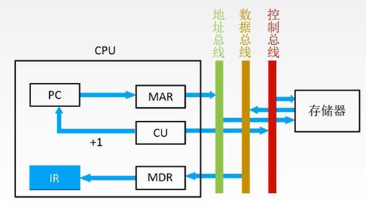
RAM:
A memory in which the contents of the storage unit can be taken out or stored as needed, and the access speed is independent of the location of the storage unit.
This kind of memory will lose its storage content in case of power failure, so it is mainly used to store programs used for a short time. According to different stored information, random access memory is divided into static random access memory (SRAM) and dynamic random access memory (DRAM).
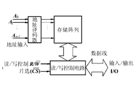
Structure block diagram of RAM
4, Experimental steps
- Verilog key code description
PC
The code is as follows:
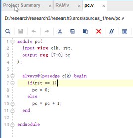
module pc(
  input  clk, rst,
  output reg [7:0] pc
);

  always@(posedge clk) begin
    if(rst == 1)
      pc = 0;
    else
      pc = pc + 1;
  end

endmodule
The code screenshot is as follows:
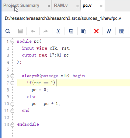
Verilog key code explanation:
Judge at each rising edge. If rst is equal to 1, set pc to 0; otherwise, pc = pc +1
RAM
The code is as follows:
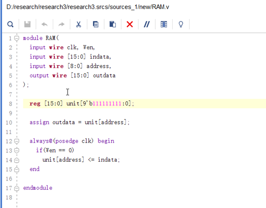
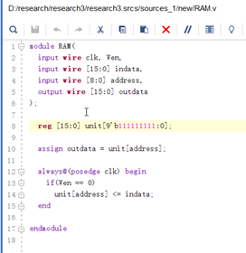
module RAM(
  input wire clk, Wen,
  input wire [15:0] indata,
  input wire [8:0] address,
  output wire [15:0] outdata
);

  reg [15:0] unit[9'b111111111:0];

  assign outdata = unit[address];

  always@(posedge clk) begin
    if(Wen == 0)
      unit[address] <= indata;
  end

endmodule
The code screenshot is as follows:
Verilog key code explanation:
The storage unit is constructed with 16 bits and 1K bytes
Judge at each rising edge. If Wen= 0, write the data to the storage unit
- Test file description
PC
The code is as follows:
module pc_simulation(
output [7:0] pc_count // Do not write default 1 bit
);
reg clk,pcs;
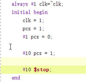
always #1 clk=~clk;
initial begin
clk = 1;
pcs = 1;
#1 pcs = 0;
#10 pcs = 1;
#10 $stop;
end
pc try(
.clk(clk),
.pcs(pcs),
.pc_count(pc_count)
);
endmodule
The screenshot of key codes of the test file is as follows:

Interpretation of key codes in test documents:
Flip the clk clock every 1ns, and set clk = 1 and pcs = 1 at the beginning
pcs = 1 after 1ns
pcs = 1 after 10ns
RAM
The code is as follows:
module RAM_simulation(
output [15:0] outdata
);
reg [9:0] address;
reg clk,Wen;
reg [15:0] indata;
always #5 clk=~clk;
integer i;
initial clk = 0;
initial begin
clk = 0;
Wen = 1;
#10;
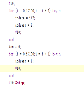
for (i = 0;i<100;i = i + 1) begin
indata = i*2;
address = i;
#10;
end
Wen = 0;
for (i = 0;i<100;i = i + 1) begin
address = i;
#10;
end
#10 $stop;
end
RAM try(
.clk(clk),
.Wen(Wen),
.address(address),
.outdata(outdata),
.indata(indata)
);
endmodule
The screenshot of key codes of the test file is as follows:

Interpretation of key codes in test documents:
We fill in the number of 2*i (a total of 100) on the storage unit with address i
Then set Wen to 0, that is, it is not writable
Then continuously set the address verification
- ModelSim simulation (including simulation analysis and summary)
PC


Combined with our verilog language and test files
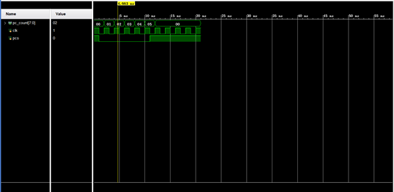
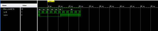
In the first 12 ns, pc is constantly + 1.;
In the 11ns, we set pcs to 0, that is, set pc to 0 at the next rising edge.
According to the ModelSim simulation diagram, we can see that our experiment is successful
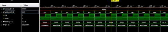
RAM
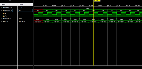
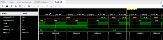

Combined with our verilog language and test files, the simulation diagram shows that
In the first 1000 ns, we are constantly writing numbers
After 1000 ns, change the address to achieve digital verification
5, Summary
PC
Verilog is used to complete the design of program counter PC, and PC is an 8-bit counter
Corresponding test documents have been prepared,
Flip the clk clock every 1ns, and set clk = 1 and pcs = 1 at the beginning
pcs = 1 after 1ns
pcs = 1 after 10ns
Combined with ModelSim simulation file, we can know the success of the experiment
RAM
Verilog is used to complete the design of data memory. Its storage word length is 16 bits and storage capacity is 1K bytes. A read-write control signal line controls reading and writing, and the low level is effective.
And prepare corresponding test documents


In the first 1000 ns, we are constantly writing numbers
After 1000 ns, change the address to achieve digital verification
Combined with ModelSim simulation file, we can know the success of the experiment