STM32 multi-channel ADC sampling to obtain analog output data of GY-25A inclination sensor
GY-25A module is a new type of inclination sensor module, which has the functions of X-axis and Y-axis analog angle output and serial port angle output. This paper introduces that STM32 obtains the angle data of GY-25A analog output and adopts the multi-channel ADC mode with power supply voltage calibration.

Introduction to analog output format
The power supply voltage of the module is 3.3V ~ 5V, and the built-in LDO output 3.3V supplies power to the chip, so the output of the chip takes 3.3V as the reference. The voltage values of the two analog voltages output by the x-axis and Y-axis of the module are in the range of 0 ~ 3.3V.
Roll angle rollover characteristics
The rolling angle variation relationship of the chip is as follows:
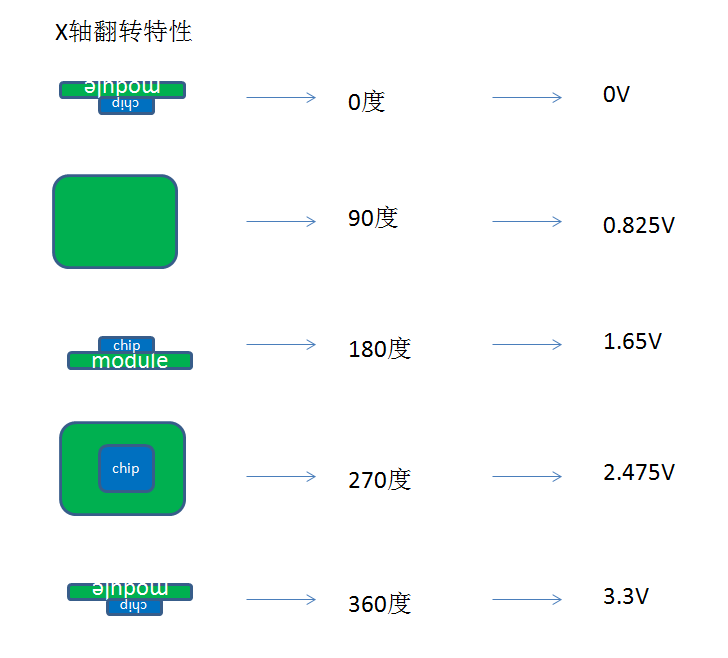
It should be noted that when the chip is facing down and the module is parallel to the horizontal plane, the X-axis of the chip will jog, and there will be a jump between 0V output and 3.3V output!
The above is the output characteristics of roll angle X axis.
Pitch angle flip characteristic
The pitch angle variation relationship of the chip is as follows:
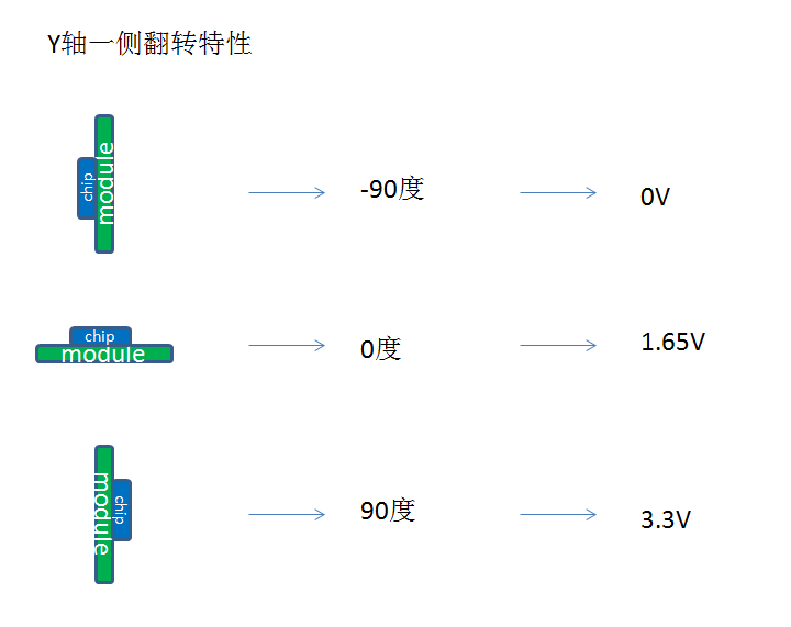

From the output characteristics of roll angle and pitch angle, it can be seen that roll angle is a 360 degree resolution characteristic and pitch angle is a 180 degree resolution characteristic, which is consistent with the origin of the name.
STM32 multichannel ADC program
Here, the STM32F401CCU6 development board is used to introduce the way of ADC sampling to obtain GY-25A analog output voltage.
Introduce the project of establishing HAL library through stm32subeide:
First, establish the project and configure the clock. For ordinary timing, the internal clock can be used.

Select PA0 and PA1 as ADC sampling analog input channel, and select reference voltage input channel:
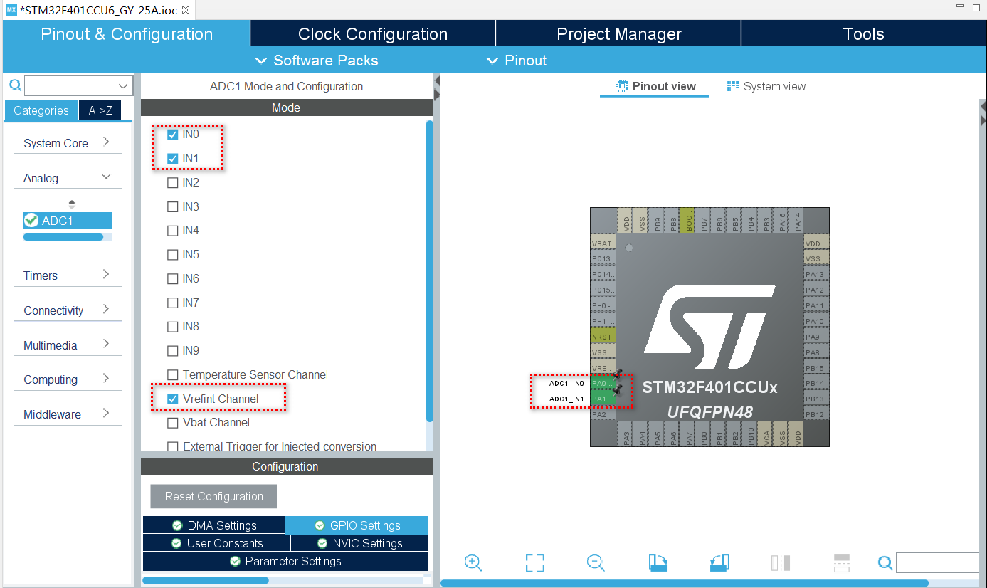
Set sampling parameters, including sampling frequency, resolution and data output alignment. Here, scanning mode and discontinuous conversion mode are adopted, and one conversion trigger is set to sample only one channel. DMA receiving mode is not adopted. And set the end flag generated after single channel sampling conversion.

Here, the priority control mode is not required, but the conventional conversion mode is adopted. The reference voltage channel vreint, channel 0 (connected to the X-axis analog output of the inclination sensor) and channel 1 (connected to the Y-axis analog output of the inclination sensor) are listed as conversion channels in order:

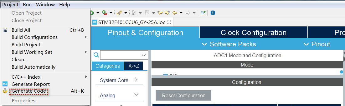
Generate project initial file:
Write code to realize multi-channel ADC sampling with reference voltage calibration:
/* USER CODE BEGIN Header */
/**
  ******************************************************************************
  * @file           : main.c
  * @brief          : Main program body
  ******************************************************************************
  * @attention
  *
  * Copyright (c) 2022 STMicroelectronics.
  * All rights reserved.
  *
  * This software is licensed under terms that can be found in the LICENSE file
  * in the root directory of this software component.
  * If no LICENSE file comes with this software, it is provided AS-IS.
  *
  ******************************************************************************
  */
/* USER CODE END Header */
/* Includes ------------------------------------------------------------------*/
#include "main.h"

/* Private includes ----------------------------------------------------------*/
/* USER CODE BEGIN Includes */

/* USER CODE END Includes */

/* Private typedef -----------------------------------------------------------*/
/* USER CODE BEGIN PTD */

/* USER CODE END PTD */

/* Private define ------------------------------------------------------------*/
/* USER CODE BEGIN PD */
/* USER CODE END PD */

/* Private macro -------------------------------------------------------------*/

/* USER CODE END PM */

/* Private variables ---------------------------------------------------------*/
ADC_HandleTypeDef hadc1;

/* USER CODE BEGIN PV */

/* USER CODE END PV */

/* Private function prototypes -----------------------------------------------*/
void SystemClock_Config(void);
static void MX_GPIO_Init(void);
static void MX_ADC1_Init(void);
/* USER CODE BEGIN PFP */

/* USER CODE END PFP */

/* Private user code ---------------------------------------------------------*/
/* USER CODE BEGIN 0 */
uint16_t i_VDD_CALI ;
uint16_t ADCV[3];
uint16_t ADCV_AVG[3];

/* USER CODE BEGIN PM */
void GET_ADC(void) {
	HAL_StatusTypeDef adc_polling_status;

	__HAL_RCC_ADC1_CLK_ENABLE();
	//Wait for the VREFINT used by ADC ready
	while (__HAL_PWR_GET_FLAG(PWR_FLAG_VOSRDY) == RESET) ;
	HAL_ADC_Stop(&hadc1);

	ADCV[0]=0xffff;ADCV[1]=0xffff;ADCV[2]=0xffff;

	//Start conversion
	HAL_ADC_Start(&hadc1);
	//Wait for for the end of conversion
	adc_polling_status = HAL_ADC_PollForConversion(&hadc1, 20); // overtime 20ms

	if (adc_polling_status == HAL_OK)
	{
		ADCV[0] = HAL_ADC_GetValue(&hadc1); //Vref
	}
	else
	{
		HAL_ADC_Stop(&hadc1);
		__HAL_RCC_ADC1_CLK_DISABLE();
		return;
	}

	//Start conversion
	HAL_ADC_Start(&hadc1);
	//Wait for for the end of conversion
	adc_polling_status = HAL_ADC_PollForConversion(&hadc1, 20); // overtime 20ms
	if (adc_polling_status == HAL_OK)
	{
		//ADCV[1] = HAL_ADC_GetValue(&hadc1); //Channel 0 w/o Vref correction
		ADCV[1] = (uint16_t)(HAL_ADC_GetValue(&hadc1)*(((double)i_VDD_CALI)/ADCV[0])); //Channel 0 w/ Vref correction
	}
	else
	{
		HAL_ADC_Stop(&hadc1);
		__HAL_RCC_ADC1_CLK_DISABLE();
		return;
	}

	//Start conversion
	HAL_ADC_Start(&hadc1);
	//Wait for for the end of conversion
	adc_polling_status = HAL_ADC_PollForConversion(&hadc1, 20); // overtime 20ms
	if (adc_polling_status == HAL_OK)
	{
		//ADCV[2] = HAL_ADC_GetValue(&hadc1);  //Channel 1 w/o Vref correction
		ADCV[2] = (uint16_t)(HAL_ADC_GetValue(&hadc1)*(((double)i_VDD_CALI)/ADCV[0])); //Channel 1 w/ Vref correction
	}
	else
	{
		HAL_ADC_Stop(&hadc1);
		__HAL_RCC_ADC1_CLK_DISABLE();
		return;
	}

	//Stop
	HAL_ADC_Stop(&hadc1);
	__HAL_RCC_ADC1_CLK_DISABLE();
}

void GET_ADC_AVG(uint32_t times) {
	uint64_t adc_acc0 = 0, adc_acc1=0, adc_acc2=0;
	uint32_t adc_conv0 = 0 ,adc_conv1 = 0 , adc_conv2 = 0;

	HAL_StatusTypeDef adc_polling_status;
	uint32_t i=0, j=0;

	__HAL_RCC_ADC1_CLK_ENABLE();
	//Wait for the VREFINT used by ADC ready
	while (__HAL_PWR_GET_FLAG(PWR_FLAG_VOSRDY) == RESET) ;
	HAL_ADC_Stop(&hadc1);

	for (i = 0; i < times; i++) {
		//Start conversion
		HAL_ADC_Start(&hadc1);
		//Wait for conversion end
		adc_polling_status = HAL_ADC_PollForConversion(&hadc1, 20); // overtime 20ms

		if (adc_polling_status == HAL_OK) {
			//read data
			adc_acc0 = (uint64_t) HAL_ADC_GetValue(&hadc1);
		}
		else
		{
			continue;
		}

		//Start conversion
		HAL_ADC_Start(&hadc1);
		//Wait for conversion end
		adc_polling_status = HAL_ADC_PollForConversion(&hadc1, 20); // overtime 20ms
		if (adc_polling_status == HAL_OK) {
			//read data
			adc_acc1 = (uint64_t) HAL_ADC_GetValue(&hadc1);

		}
		else
		{
			continue;
		}

		//Start conversion
		HAL_ADC_Start(&hadc1);
		//Wait for conversion end
		adc_polling_status = HAL_ADC_PollForConversion(&hadc1, 20); // overtime 20ms
		if (adc_polling_status == HAL_OK) {
			//read data
			adc_acc2 = (uint64_t) HAL_ADC_GetValue(&hadc1);

			adc_conv0 += (uint32_t)adc_acc0;
			adc_conv1 += (uint32_t)(adc_acc1*(((double)i_VDD_CALI)/adc_acc0));
			adc_conv2 += (uint32_t)(adc_acc2*(((double)i_VDD_CALI)/adc_acc0));

			j++;
		}
		else
		{
			continue;
		}

	}
	// Stop
	HAL_ADC_Stop(&hadc1);
	__HAL_RCC_ADC1_CLK_DISABLE();

	ADCV_AVG[0] = adc_conv0/j;
	ADCV_AVG[1] = adc_conv1/j;
	ADCV_AVG[2] = adc_conv2/j;

	return ;

}
/* USER CODE END 0 */

/**
  * @brief  The application entry point.
  * @retval int
  */
int main(void)
{
  /* USER CODE BEGIN 1 */
 i_VDD_CALI = (*((uint16_t *)(0x1FFF7A2A)));
  /* USER CODE END 1 */

  /* MCU Configuration--------------------------------------------------------*/

  /* Reset of all peripherals, Initializes the Flash interface and the Systick. */
  HAL_Init();

  /* USER CODE BEGIN Init */

  /* USER CODE END Init */

  /* Configure the system clock */
  SystemClock_Config();

  /* USER CODE BEGIN SysInit */

  /* USER CODE END SysInit */

  /* Initialize all configured peripherals */
  MX_GPIO_Init();
  MX_ADC1_Init();
  /* USER CODE BEGIN 2 */

  /* USER CODE END 2 */

  /* Infinite loop */
  /* USER CODE BEGIN WHILE */
  while (1)
  {

	  GET_ADC();
	  HAL_Delay(10);
	  GET_ADC_AVG(10000) ;
	  HAL_Delay(10);

    /* USER CODE END WHILE */

    /* USER CODE BEGIN 3 */
  }
  /* USER CODE END 3 */
}

/**
  * @brief System Clock Configuration
  * @retval None
  */
void SystemClock_Config(void)
{
  RCC_OscInitTypeDef RCC_OscInitStruct = {0};
  RCC_ClkInitTypeDef RCC_ClkInitStruct = {0};

  /** Configure the main internal regulator output voltage
  */
  __HAL_RCC_PWR_CLK_ENABLE();
  __HAL_PWR_VOLTAGESCALING_CONFIG(PWR_REGULATOR_VOLTAGE_SCALE2);
  /** Initializes the RCC Oscillators according to the specified parameters
  * in the RCC_OscInitTypeDef structure.
  */
  RCC_OscInitStruct.OscillatorType = RCC_OSCILLATORTYPE_HSI;
  RCC_OscInitStruct.HSIState = RCC_HSI_ON;
  RCC_OscInitStruct.HSICalibrationValue = RCC_HSICALIBRATION_DEFAULT;
  RCC_OscInitStruct.PLL.PLLState = RCC_PLL_ON;
  RCC_OscInitStruct.PLL.PLLSource = RCC_PLLSOURCE_HSI;
  RCC_OscInitStruct.PLL.PLLM = 16;
  RCC_OscInitStruct.PLL.PLLN = 168;
  RCC_OscInitStruct.PLL.PLLP = RCC_PLLP_DIV2;
  RCC_OscInitStruct.PLL.PLLQ = 4;
  if (HAL_RCC_OscConfig(&RCC_OscInitStruct) != HAL_OK)
  {
    Error_Handler();
  }
  /** Initializes the CPU, AHB and APB buses clocks
  */
  RCC_ClkInitStruct.ClockType = RCC_CLOCKTYPE_HCLK|RCC_CLOCKTYPE_SYSCLK
                              |RCC_CLOCKTYPE_PCLK1|RCC_CLOCKTYPE_PCLK2;
  RCC_ClkInitStruct.SYSCLKSource = RCC_SYSCLKSOURCE_PLLCLK;
  RCC_ClkInitStruct.AHBCLKDivider = RCC_SYSCLK_DIV1;
  RCC_ClkInitStruct.APB1CLKDivider = RCC_HCLK_DIV2;
  RCC_ClkInitStruct.APB2CLKDivider = RCC_HCLK_DIV1;

  if (HAL_RCC_ClockConfig(&RCC_ClkInitStruct, FLASH_LATENCY_2) != HAL_OK)
  {
    Error_Handler();
  }
}

/**
  * @brief ADC1 Initialization Function
  * @param None
  * @retval None
  */
static void MX_ADC1_Init(void)
{

  /* USER CODE BEGIN ADC1_Init 0 */

  /* USER CODE END ADC1_Init 0 */

  ADC_ChannelConfTypeDef sConfig = {0};

  /* USER CODE BEGIN ADC1_Init 1 */

  /* USER CODE END ADC1_Init 1 */
  /** Configure the global features of the ADC (Clock, Resolution, Data Alignment and number of conversion)
  */
  hadc1.Instance = ADC1;
  hadc1.Init.ClockPrescaler = ADC_CLOCK_SYNC_PCLK_DIV4;
  hadc1.Init.Resolution = ADC_RESOLUTION_12B;
  hadc1.Init.ScanConvMode = ENABLE;
  hadc1.Init.ContinuousConvMode = DISABLE;
  hadc1.Init.DiscontinuousConvMode = ENABLE;
  hadc1.Init.NbrOfDiscConversion = 1;
  hadc1.Init.ExternalTrigConvEdge = ADC_EXTERNALTRIGCONVEDGE_NONE;
  hadc1.Init.ExternalTrigConv = ADC_SOFTWARE_START;
  hadc1.Init.DataAlign = ADC_DATAALIGN_RIGHT;
  hadc1.Init.NbrOfConversion = 3;
  hadc1.Init.DMAContinuousRequests = DISABLE;
  hadc1.Init.EOCSelection = ADC_EOC_SINGLE_CONV;
  if (HAL_ADC_Init(&hadc1) != HAL_OK)
  {
    Error_Handler();
  }
  /** Configure for the selected ADC regular channel its corresponding rank in the sequencer and its sample time.
  */
  sConfig.Channel = ADC_CHANNEL_VREFINT;
  sConfig.Rank = 1;
  sConfig.SamplingTime = ADC_SAMPLETIME_3CYCLES;
  if (HAL_ADC_ConfigChannel(&hadc1, &sConfig) != HAL_OK)
  {
    Error_Handler();
  }
  /** Configure for the selected ADC regular channel its corresponding rank in the sequencer and its sample time.
  */
  sConfig.Channel = ADC_CHANNEL_0;
  sConfig.Rank = 2;
  if (HAL_ADC_ConfigChannel(&hadc1, &sConfig) != HAL_OK)
  {
    Error_Handler();
  }
  /** Configure for the selected ADC regular channel its corresponding rank in the sequencer and its sample time.
  */
  sConfig.Channel = ADC_CHANNEL_1;
  sConfig.Rank = 3;
  if (HAL_ADC_ConfigChannel(&hadc1, &sConfig) != HAL_OK)
  {
    Error_Handler();
  }
  /* USER CODE BEGIN ADC1_Init 2 */

  /* USER CODE END ADC1_Init 2 */

}

/**
  * @brief GPIO Initialization Function
  * @param None
  * @retval None
  */
static void MX_GPIO_Init(void)
{

  /* GPIO Ports Clock Enable */
  __HAL_RCC_GPIOA_CLK_ENABLE();

}

/* USER CODE BEGIN 4 */

/* USER CODE END 4 */

/**
  * @brief  This function is executed in case of error occurrence.
  * @retval None
  */
void Error_Handler(void)
{
  /* USER CODE BEGIN Error_Handler_Debug */
  /* User can add his own implementation to report the HAL error return state */
  __disable_irq();
  while (1)
  {
  }
  /* USER CODE END Error_Handler_Debug */
}

#ifdef  USE_FULL_ASSERT
/**
  * @brief  Reports the name of the source file and the source line number
  *         where the assert_param error has occurred.
  * @param  file: pointer to the source file name
  * @param  line: assert_param error line source number
  * @retval None
  */
void assert_failed(uint8_t *file, uint32_t line)
{
  /* USER CODE BEGIN 6 */
  /* User can add his own implementation to report the file name and line number,
     ex: printf("Wrong parameters value: file %s on line %d\r\n", file, line) */
  /* USER CODE END 6 */
}
#endif /* USE_FULL_ASSERT */
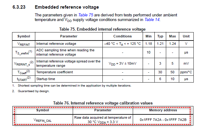
Where, by variable i_VDD_CALI reads the parameter values in the chip that are tested and configured by ST company when leaving the factory. After reading the real-time power supply voltage through ADC, Cali calibrates the signal voltage read by channel 0 and channel 1. i_ VDD_ The value storage address of Cali comes from the data manual:
Among them, ADCV[0], ADCV[1], ADCV[2] are respectively used to store the power supply voltage of single ADC sampling and the voltage values of channel 0 and channel 1. Call GET_ADC() implements sampling.
Where ADCV_AVG[0], ADCV_AVG[1], ADCV_AVG[2] is used to store the power supply voltage after multiple ADC sampling average, as well as the voltage values of channel 0 and channel 1. Call GET_ADC_AVG(times) implements sampling, and times specifies the cumulative number of samples.
A simple loop read operation is implemented in the while loop.
–End–