catalogue
1, Hardware circuit

2, DS1302
1.DS1302 overview
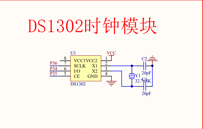
DS1302 is a trickle charging clock chip launched by DALLAS company. It contains a real-time clock / calendar and 31 byte static RAM. It communicates with the single chip microcomputer through a simple serial interface. The real-time clock / calendar circuit provides the information of seconds, minutes, hours, days, weeks, months and years, and the number of days of each month and leap years can be adjusted automatically. The clock operation can be indicated by AM/PM. The DS1302 and MCU can simply communicate in synchronous serial mode. The simple three wire SPI communication mode: ① RES reset ② I/O data line ③ SCLK serial clock.
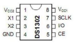
1. VCC2: main power pin
2. X1 and X2: DS1302 external crystal oscillator pins, which usually need to be externally connected with 32.768K crystal oscillator
3. GND: power ground
4. CE: the enable pin is also the reset pin (the function of the new version is changed).
5. I/O: serial data pin. Data output or input is from this pin
6. SCLK: serial clock pin
7. VCC1: standby power supply
2.ds1302 control register
It is used to store the control DS1302 command. This register can be controlled to control operations such as selective read or write.
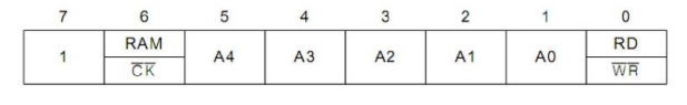
1. The 7th bit is fixed as 1
2. Bit 6, 1 refers to address internal memory address ram, and 0 refers to address internal register, that is, the memory of month, year and day, which is generally set to 0
3. Address of bit 5 to bit 1 and bit 6 memory
4. Bit 0, bit 1, read operation, and 0 is write operation
The details are shown in the figure below.
3.DS1302 sequence diagram

CE: reset sequence
SCLK: clock timing
IO: data transmission timing
Note: both DS1302 and DS18B20 transmit (read / write) data from low to high, which should be paid attention to during programming.
(1) Byte Reader:
/*Read byte*/
u8 ds1302_read_byte(u8 addr) //Meaning of addr: users need to read data from a register. Addr is the address of this register
{
	u8 i=0,t=0,dat=0,x=0;
	CE=0;
	_nop_();
	SCLK=0;
	_nop_();
	CE=1;
	for(i=0;i<8;i++)
	{
		t=addr<<7;
		IO=t>>7;
		SCLK=1;
		_nop_();
		SCLK=0;
		_nop_();
		addr>>=1;
	}
	for(i=0;i<8;i++)
	{
		SCLK=1;
		_nop_();
		dat>>=1;
		x=IO;
		SCLK=0;
		_nop_();
		dat=dat|(x<<7);

	}
	CE=0;
	_nop_();
//The meaning of the following code: because the IO port of the single chip microcomputer used by the author has no pull-up resistance, it needs to pull-up level artificially.
	IO=0;
	_nop_();
	IO=1;
	_nop_();
	return dat;
}
(2) Byte writing program
/*Write byte*/
void ds1302_write_byte(u8 addr,u8 dat)//dat meaning: data to be written
{                                     //Meaning of addr: users need to write data to a register. Addr is the address of this register
	u8 i=0,t=0;
	CE=0;
	_nop_();
	SCLK=0;
	_nop_();
	CE=1;
	_nop_();
	for(i=0;i<8;i++)
	{
		t=addr<<7;
		IO=t>>7;
		SCLK=1;
		_nop_();
		SCLK=0;
		_nop_();
		addr>>=1;
	}
		for(i=0;i<8;i++)
	{
		t=dat<<7;
		IO=t>>7;
		SCLK=1;
		_nop_();
		SCLK=0;
		_nop_();
		dat>>=1;
	}
	CE=0;
}
(3) Initialization procedure
/*This function is used to set the initial time, such as 13:30:59*/
void ds1302_init(void)
{
	u8 i=0;
	ds1302_write_byte(0x8e,0x00);
	for(i=0;i<7;i++)//Write initial time
	{
		ds1302_write_byte(gWRITE_RTC_ARRD[i],gDS1302_TIME[i]);
	}
	ds1302_write_byte(0x8e,0x80);
}
gWRITE_RTC_ARRD[]Is the address of the read register
(4) Conversion time program
void ds1302_read_time(void)
{
u8 i=0;
for(i=0;i<7;i++)
{
gDS1302_TIME[i]=ds1302_read_byte(gREAD_RTC_ARRD[i]);
}
}
//gDS1302_TIME [] is the BCD code corresponding to time
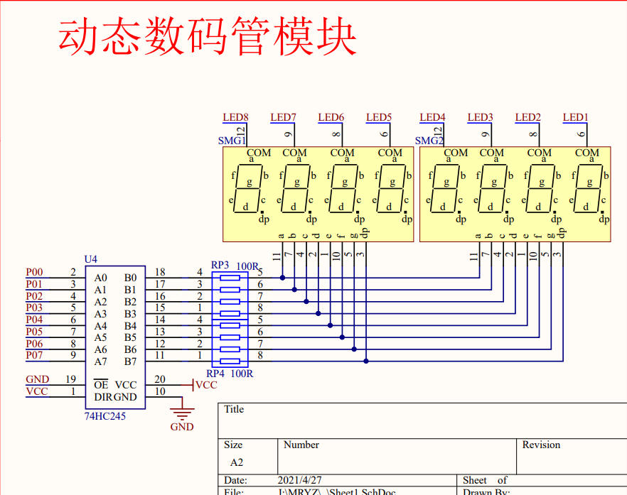
//gREAD_RTC_ARRD [] is the address of the read registerIII. nixie tube
void smg_display(u8 dat[],u8 pos)//dat array elements are hexadecimal numbers corresponding to numbers
{                                //pos is the number of nixie tubes that start to light up
	u8 i=0;
	u8 pos_temp=pos-1;
	for(i=pos_temp;i<8;i++)
	{
	   	switch(i)//Bit selection
		{
			case 0: LSC=1;LSB=1;LSA=1;break;
			case 1: LSC=1;LSB=1;LSA=0;break;
			case 2: LSC=1;LSB=0;LSA=1;break;
			case 3: LSC=1;LSB=0;LSA=0;break;
			case 4: LSC=0;LSB=1;LSA=1;break;
			case 5: LSC=0;LSB=1;LSA=0;break;
			case 6: LSC=0;LSB=0;LSA=1;break;
			case 7: LSC=0;LSB=0;LSA=0;break;
		}
		SMG_A_DP_PORT=dat[i-pos_temp];
		delay_10us(100);
		SMG_A_DP_PORT=0x00;
	}
}
IV. main program
void main()
{
	u8 num[8];
	ds1302_init();
	while(1)
	{
	 	ds1302_read_time();


		num[0]=gsmg_code[gDS1302_TIME[2]/16];
		num[1]=gsmg_code[gDS1302_TIME[2]%16];
		num[2]=0x40;
		num[3]=gsmg_code[gDS1302_TIME[1]/16];
		num[4]=gsmg_code[gDS1302_TIME[1]%16];
		num[5]=0x40;
		num[6]=gsmg_code[gDS1302_TIME[0]/16];
		num[7]=gsmg_code[gDS1302_TIME[0]%16];
		smg_display(num,1);
	}

}