Introduction
After entering the national competition, the expansion board is also an important part. Some of the above things are also the first contact, so take this opportunity to record the learning process and help you mine.
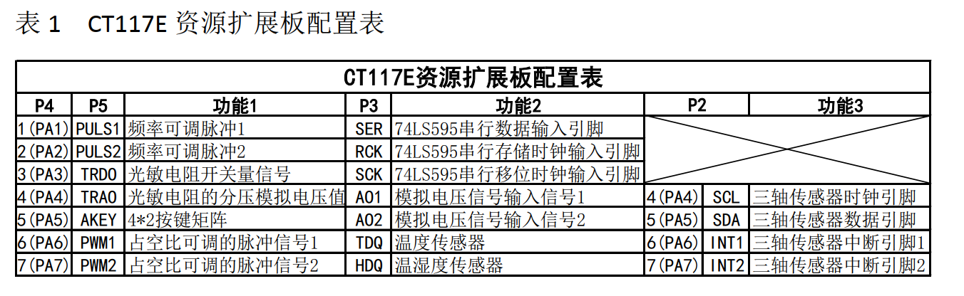
The resources on the expansion board are roughly divided into: nixie tube, ADC key, photosensitive resistance, temperature sensor, temperature and humidity sensor, triaxial acceleration sensor, two ways of duty cycle adjustable PWM, two ways of frequency adjustable PWM (for input capture) and two ways of ADC input.
It looks like a lot. In fact, the PWM and analog signal output parts can be realized without programming hardware. The acquisition and ADC can use the previous knowledge. The key and photoresist are also based on the principle of ADC part, which is slightly modified. In this way, the task is simplified and learning is much easier.
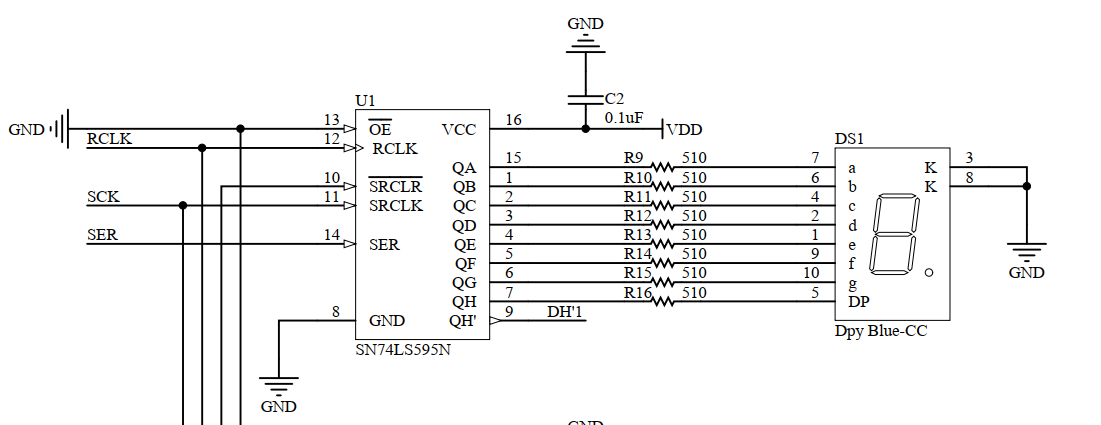
Digital tube
The expansion board has three nixie tubes, which are realized by 74LS595 shift register. After configuration, it can be realized by operating ser (serial data input pin), SCK (serial shift clock input pin) and RCK (traversal storage shift clock input).
Jumper cap: SER, SCK and RCK of P3 are connected with P4 correspondingly
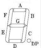
I personally understand the purpose of the three pins: SER is to operate the nixie tube position, which can be understood as controlling a certain section of A-G to turn on or off
SCK is used for shifting. When the falling edge of SCK is shifted, the data is valid
RCK sends the shifted data to the hardware at the falling edge.
Operation process:
code
SER, RCK and SCK correspond to PA1, PA2 and PA3 respectively, and the push-pull output mode can be configured
macros predefined
#ifndef _SEG_H_
#define _SEG_H_

#include "stm32f10x.h"

#define SER_H	GPIO_SetBits(GPIOA,GPIO_Pin_1)
#define SER_L	GPIO_ResetBits(GPIOA,GPIO_Pin_1)
#define RCK_H	GPIO_SetBits(GPIOA,GPIO_Pin_2)
#define RCK_L	GPIO_ResetBits(GPIOA,GPIO_Pin_2)
#define SCK_H	GPIO_SetBits(GPIOA,GPIO_Pin_3)
#define SCK_L	GPIO_ResetBits(GPIOA,GPIO_Pin_3)

void Seg_Init(void);
void Seg_Write(u8 N1,u8 N2,u8 N3);


#endif
function
#include "seg.h"

u8 Seg7[17] = { 0x3f,0x06,0x5b,0x4f, 0x66,0x6d,0x7d,0x07,0x7f,0x6f,0x77,0x7c, 0x39,0x5e,0x79,0x71,0x00};

void Seg_Init(void)
{
	GPIO_InitTypeDef GPIO_InitStructure;

	RCC_APB2PeriphClockCmd(RCC_APB2Periph_GPIOA, ENABLE);

	GPIO_InitStructure.GPIO_Pin = GPIO_Pin_1 | GPIO_Pin_2 | GPIO_Pin_3;
	GPIO_InitStructure.GPIO_Speed = GPIO_Speed_50MHz;
	GPIO_InitStructure.GPIO_Mode = GPIO_Mode_Out_PP;
	GPIO_Init(GPIOA, &GPIO_InitStructure);
}

void Seg_Write(u8 N1,u8 N2,u8 N3)
{
	u8 num,i;
	num = Seg7[N3];
	for(i=0;i<8;i++)
	{
		if(num&0x80)	SER_H;
		else	SER_L;
		SCK_H;
		num <<= 1;
		SCK_L;
	}
	num = Seg7[N2];
	for(i=0;i<8;i++)
	{
		if(num&0x80)	SER_H;
		else	SER_L;
		SCK_H;
		num <<= 1;
		SCK_L;
	}
	num = Seg7[N1];
	for(i=0;i<8;i++)
	{
		if(num&0x80)	SER_H;
		else	SER_L;
		SCK_H;
		num <<= 1;
		SCK_L;
	}
	RCK_H;
	RCK_L;

}
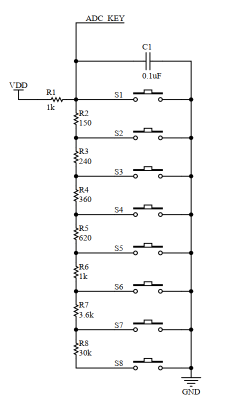
ADC key
ADC button is actually based on the principle of partial voltage. It can be regarded as ADC, but it can not be regarded as a button. In fact, only one IO is used, but multiple keys can be detected to save resources. (I don't know if the National Games will directly use him as a button)
Principle: when each key is pressed, due to different partial voltage resistance values, the input analog signals are different. You only need to judge the range of the input analog signal value.
Jumper cap: AKEY of P3 is connected with P4 correspondingly
code
macros predefined
#define AdcKey1		1
#define AdcKey2		2
#define AdcKey3		3
#define AdcKey4		4
#define AdcKey5		5
#define AdcKey6		6
#define AdcKey7		7
#define AdcKey8		8
function
#include "adckey.h"
#include "stdio.h"
#include "lcd.h"

void ADCkey_Init(void)
{
	GPIO_InitTypeDef GPIO_InitStructure;
	ADC_InitTypeDef ADC_InitStructure;

	RCC_APB2PeriphClockCmd(RCC_APB2Periph_ADC1 | RCC_APB2Periph_GPIOA, ENABLE);

	GPIO_InitStructure.GPIO_Pin = GPIO_Pin_5;
	GPIO_InitStructure.GPIO_Mode = GPIO_Mode_AIN;
	GPIO_Init(GPIOA, &GPIO_InitStructure);

	ADC_InitStructure.ADC_Mode = ADC_Mode_Independent;
	ADC_InitStructure.ADC_ScanConvMode = DISABLE;
	ADC_InitStructure.ADC_ContinuousConvMode = DISABLE;
	ADC_InitStructure.ADC_ExternalTrigConv = ADC_ExternalTrigConv_None;
	ADC_InitStructure.ADC_DataAlign = ADC_DataAlign_Right;
	ADC_InitStructure.ADC_NbrOfChannel = 2;
	ADC_Init(ADC1, &ADC_InitStructure);

	ADC_Cmd(ADC1, ENABLE);

	ADC_ResetCalibration(ADC1);
	while(ADC_GetResetCalibrationStatus(ADC1));

	ADC_StartCalibration(ADC1);
	while(ADC_GetCalibrationStatus(ADC1));

}

u16 Get_Adc(void)
{
	u16 Value;

	ADC_RegularChannelConfig(ADC1, ADC_Channel_5, 1, ADC_SampleTime_55Cycles5);
	ADC_SoftwareStartConvCmd(ADC1, ENABLE);
	while(!ADC_GetFlagStatus(ADC1,ADC_FLAG_EOC));

	Value=ADC_GetConversionValue(ADC1);


	ADC_SoftwareStartConvCmd(ADC1, DISABLE);

	return Value;
}

u8 Key_Compare(void)
{
	u16 value;
	u8 str[20];
	value =	Get_Adc();
	sprintf((char*)str,"    Key_Val : %d     ",value);
	LCD_DisplayStringLine(Line6,str);
	if(value<500)	return AdcKey1;
	else if(value>500&&value<1000)	return AdcKey2;
	else if(value>1000&&value<1500)	return AdcKey3;
	else if(value>1500&&value<2000)	return AdcKey4;
	else if(value>2000&&value<2800)	return AdcKey5;
	else if(value>2800&&value<3300)	return AdcKey6;
	else if(value>3300&&value<3800)	return AdcKey7;
	else	return AdcKey8;

}
Final supplement
ADC keys can also be seen from the code. I have displayed the ADC value, so that you can roughly delimit the range of detection keys by pressing each key. Compared with memorizing the interval directly, it is more stable even if you change other boards, and debugging is fast.
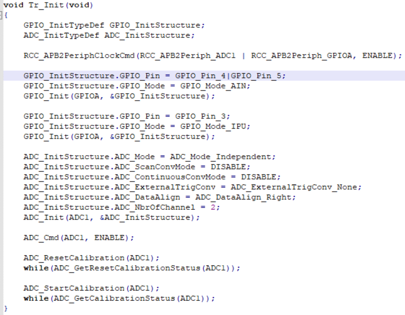
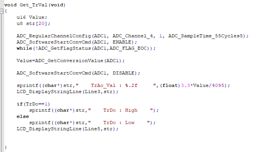
As for the ADC part, after learning the photoresist, I use it together with the ADC key (Channel 4 and channel 5), which are initialized respectively. However, there is a problem that two data displays are reversed. The ADC key value displayed by the photoresist value changes the value displayed by the photoresist when the key is pressed. However, if two channels operate separately, one of them will return to normal.
Solution: two channels are initialized in the same function in ADC