4.6 EEPROM memory chip (AT24C02)
4.6.1 introduction to schematic diagram
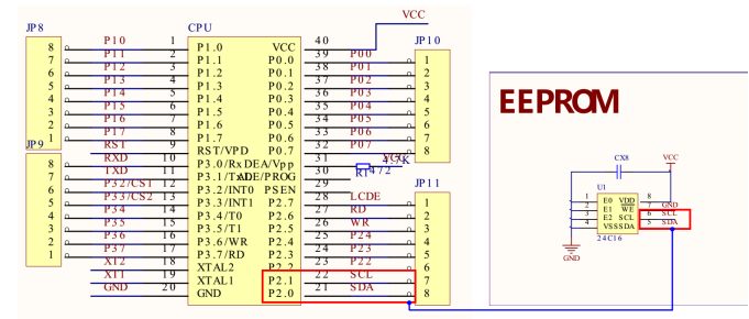
Figure 4-6-1
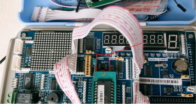
Figure 4-6-2
The EEPROM model on the experimental board is AT24C02N, and the communication interface is IIC, which is connected to P2.1(SCL) and P2.2(SDA) ports of single chip microcomputer.
AT24C02 is a 2kbit (256 byte) EEPROM.
The schematic diagram of the experimental board is 24C16, and the specific chip model used on the actual experimental board is AT24C02.
4.6.2 introduction to AT24C02
AT24C02 is a 2K Bit Serial EEPROM with 256 byte space. AT24C02 has an 8-byte page write buffer inside. The device operates through IIC bus interface and has a special write protection function.
I2C bus is a two-wire serial bus developed by Philips company, which is used to connect microcontrollers and their peripherals. It is a bus standard widely used in the field of microelectronic communication control. It is a special form of synchronous communication. It has the advantages of few interface lines, simple control mode, small device packaging form and high communication rate (this high rate refers to the communication bus with it).
characteristic:
(1) The transmission rate is 400KHz and is compatible with IIC bus
(2) 2.7V to 7V operating voltage
(3) 8-byte page write buffer
(4) 1 million erasure cycles
(5) . the data can be saved for up to 100 years
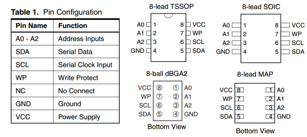
Figure 4-6-3 AT24C02 package diagram and pin function introduction
A0, A1 and A2 on the pin are address configuration pins to form eight cases of 000 ~ 111. Up to eight AT24C02 devices can be connected to the bus through device address inputs A0, A1 and A2. SDA is the data line of IIC bus and SCL is the clock line of IIC bus.
The internal device address of AT24C02 is 1010 , 2K in the following picture is the corresponding address of AT2C02.
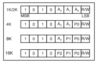
Figure 4-6-4 AT24C02 device address
A write cycle time of AT24C02 is 10ms. When the single chip microcomputer transmits data to AT24C02, AT24C02 temporarily stores the data in an 8-byte buffer. After the single chip microcomputer sends the data, it needs to wait 10ms, wait for AT24C02 to store the data in the buffer in the internal EEPROM, and the power will not be lost after it is stored in the EEPROM.

Figure 4-6-5 write cycle time
4.6.3 introduction to AT24C02 timing
(1) Bus sequence diagram

Figure 4-6-6 bus timing
(2) Start signal and stop signal sequence diagram

Fig. 4-6-7 timing of start signal and stop signal
When the clock line is at high level, the data line changes from high level to low level.
IIC_SCL=1;
IIC_SDA=1;
IIC_SDA=0;
IIC_SCL=0; //The bus starts working and starts reading and writing data
When the clock line is at high level, the data line changes from low level to high level.
IIC_SCL=0;
IIC_SDA=0;
IIC_SCL=1;
IIC_SDA=1;
(3) Response signal sequence diagram
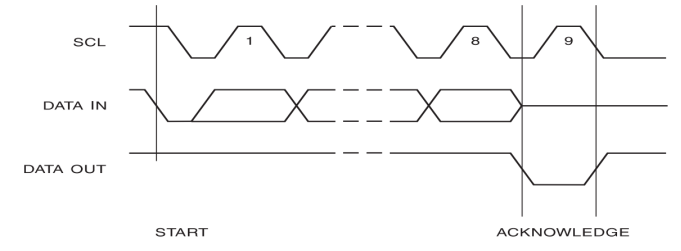
Figure 4-6-8 response sequence diagram
The effective response signal is low.
(4) Transmission sequence diagram of data bits

Figure 4-6-9 data validity
The output transmission starts from the high bit.
/*Function function:   Send a byte of data*/
void IIC_SendOneByte(u8 dat)
{
    u8 j=0,i=0;
    for(j=0;j<8;j++)
    {
        IIC_SCL=0;
        if(dat&0x80)IIC_SDA=1;
        else IIC_SDA=0;
        IIC_SCL=1;
        dat<<=1;
    }
IIC_SCL=0;
}
(5) Total timing of writing one byte to AT24C02

Figure 4-6-10
(6) Total timing of writing one page of data to AT24C02

Figure 4-6-11
(7) The total timing of reading one byte from the current address of AT24C02
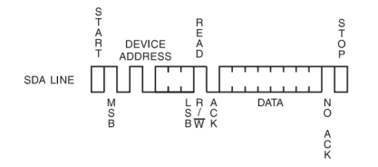
Figure 4-6-12
(8) . total timing of reading data of specified length from the specified position of AT24C02
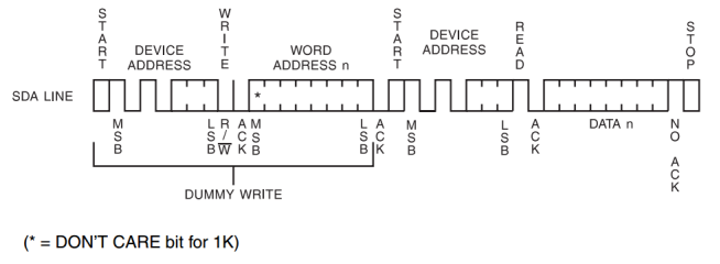
Figure 4-6-13
4.6.4 AT24C02 read / write data example code
The following code demonstrates the process of AT24C02 writing and reading data. In the main function, call the AT24C02 writing section function to store data in the specified space, then call the reading function to read it out and print it to the serial port terminal.
(description of hardware platform: CPU is STC90C516RD, crystal oscillator frequency is 12MHZ, working in 12T mode, and one machine cycle is 1us time)
Example code:
#include <reg51.h>
/*
explain:   In 12MHZ crystal oscillator and 12T mode, the time consumed by i + + is almost 12us
*/
/*
Hardware connection:
    SCL---P2.1
    SDA---P2.0
*/
//data line
sbit IIC_SDA=P2^0;
//Clock line
sbit IIC_SCL=P2^1;

/*
Function function:   Send start signal
 When the clock line is at high level, the data line changes from high level to low level
*/
void IIC_SendStart(void)
{
    u8 i=0;
    IIC_SCL=1;
    IIC_SDA=1;
    IIC_SDA=0;
    IIC_SCL=0; //The bus starts working and starts reading and writing data
}

/*
Function function:   Stop signal
 When the clock line is at high level, the data line changes from low level to high level
*/
void IIC_SendStop(void)
{
    u8 i=0;
    IIC_SCL=0;
    IIC_SDA=0;
    IIC_SCL=1;
    IIC_SDA=1;
}

/*
Function function:   Get response signal
 return   return   Value:   0 indicates that a reply has been obtained   1 means no response is obtained
*/
u8 IIC_GetAck(void)
{
    u8 i=0;
    IIC_SDA=1; //Pull up
    IIC_SCL=0;
    IIC_SCL=1;
    while(IIC_SDA)
    {
        i++;
        if(i>250)return 1; //No reply was obtained
    }
    IIC_SCL=0;
    return 0;
}

/*
Function function:   Send response signal
 Function parameter: 0 indicates response   1 means no response
*/
void IIC_SendAck(u8 ack)
{
    u8 i=0;
    IIC_SCL=0;
    if(ack)IIC_SDA=1; //Send non reply
    else IIC_SDA=0; //Send reply
    IIC_SCL=1;
    IIC_SCL=0;
}

/*
Function function:   Send a byte of data
*/
void IIC_SendOneByte(u8 dat)
{
    u8 j=0,i=0;
    for(j=0;j<8;j++)
    {
        IIC_SCL=0;
        if(dat&0x80)IIC_SDA=1;
        else IIC_SDA=0;
        IIC_SCL=1;
        dat<<=1;
    }
    IIC_SCL=0;
}

/*
Function function:   Receive one byte of data
*/
u8 IIC_RecvOneByte(void)
{
    u8 i=0,j=0;
    u8 dat=0;
    for(j=0;j<8;j++)
    {
        IIC_SCL=0;
        IIC_SCL=1;
        dat<<=1; //Indicates that 0 is received by default
        if(IIC_SDA)dat|=0x01;
    }
    IIC_SCL=0;
    return dat;
}
/*
Function function:   Write a byte
 Function parameters:
    u8 addr Location of data (0 ~ 255)
    u8 dat Data range (0 ~ 255)
*/
void AT24C02_WriteOneByte(u16 addr,u8 dat)
{
    IIC_SendStart();//Start signal
    IIC_SendOneByte(AT24C02_WRITE_ADDR);//Sending device address
    IIC_GetAck();//Get response
    IIC_SendOneByte(addr); //Address of data storage
    IIC_GetAck();//Get response
    IIC_SendOneByte(dat); //Send data to be stored
    IIC_GetAck();//Get response
    IIC_SendStop(); //Stop signal
    DelayMs(10); //Waiting to write
}

/*
Function function:   Read a byte
 Function parameters:
    u8 addr Location of data (0 ~ 255)
Return value:   Read data
*/
u8 AT24C02_ReadOneByte(u16 addr)
{
    u8 dat=0;
    IIC_SendStart();//Start signal
    IIC_SendOneByte(AT24C02_WRITE_ADDR);//Sending device address
    IIC_GetAck();//Get response
    IIC_SendOneByte(addr); //The address where the data will be read
    IIC_GetAck();//Get response

    IIC_SendStart();//Start signal
    IIC_SendOneByte(AT24C02_READ_ADDR);//Sending device address
    IIC_GetAck();//Get response
    dat=IIC_RecvOneByte();//Read data
    IIC_SendAck(1); //Send non reply
    IIC_SendStop(); //Stop signal
    return dat;
}

/*
Function function:   Reads data of the specified length from the specified location
 Function parameters:
    u16 addr Location of data (0 ~ 255)
    u16 len Read length
    u8 *buffer Store read data
 Return value:   Read data
*/
void AT24C02_ReadByte(u16 addr,u16 len,u8 *buffer)
{
    u16 i=0;
    IIC_SendStart();//Start signal
    IIC_SendOneByte(AT24C02_WRITE_ADDR);//Sending device address
    IIC_GetAck();//Get response
    IIC_SendOneByte(addr); //The address where the data will be read
    IIC_GetAck();//Get response

    IIC_SendStart();//Start signal
    IIC_SendOneByte(AT24C02_READ_ADDR);//Sending device address
    IIC_GetAck();//Get response
    for(i=0;i<len;i++)
    {
        buffer[i]=IIC_RecvOneByte();//Read data
        if(i<len-1)IIC_SendAck(0); //Send reply
        else IIC_SendAck(1); //Send non reply
    }
    IIC_SendStop(); //Stop signal
}

/*
Function function:   AT24C02 page write function
 Function parameters:
    u16 addr Write position (0 ~ 1023)
    u8 len Length written (16 bytes per page)
    u8 *buffer Store read data
*/
void AT24C02_PageWrite(u16 addr,u16 len,u8 *buffer)
{
    u16 i=0;
    IIC_SendStart();//Start signal
    IIC_SendOneByte(AT24C02_WRITE_ADDR);//Sending device address
    IIC_GetAck();//Get response
    IIC_SendOneByte(addr); //Address of data storage
    IIC_GetAck();//Get response
    for(i=0;i<len;i++)
    {
        IIC_SendOneByte(buffer[i]); //Send data to be stored
        IIC_GetAck();//Get response
    }
    IIC_SendStop(); //Stop signal
    DelayMs(10); //Waiting to write
}

/*
Function function:   Writes data of a specified length from a specified location
 Function parameters:
    u16 addr Location of data (0 ~ 255)
    u16 len Write length
    u8 *buffer Store the data to be written
 Return value:   Read data
*/
void AT24C02_WriteByte(u16 addr,u16 len,u8 *buffer)
{
    u8 page_byte=8-addr%8; //Gets the number of bytes remaining on the current page
    if(page_byte>len) //Judge whether the remaining byte space of the current page is enough to write
    {
        page_byte=len; //It means that it can be written at one time
    }
    while(1)
    {
        AT24C02_PageWrite(addr,page_byte,buffer); //Write a page
        if(page_byte==len)break; //Finished
        buffer+=page_byte; //Pointer offset
        addr+=page_byte;//Address offset
        len-=page_byte;//Get the remaining unfinished length
        if(len>8)page_byte=8;
        else page_byte=len; //You can finish it at one time
    }
}

//u8 at24c02_w[8]="1234567";
//u8 at24c02_r[8];
int main()
{
    u8 dat;
    UART_Init();        //The baud rate of initialization serial port is 4800
    while(1)
    {
//Single byte read / write test
        AT24C02_WriteOneByte(10,34);
        dat=AT24C02_ReadOneByte(10);
        printf("dat=%d\r\n",(int)dat);
        //Multiple byte read / write test
        //AT24C02_WriteByte(0,8,at24c02_w);
//        AT24C02_ReadByte(0,8,at24c02_r);
//        printf("at24c02_r=%s\r\n",at24c02_r);
          DelayMs(1000);
}
} 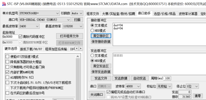
Figure 4-6-13

Fig. 4-6-14 write timing process detected by logic analyzer

Fig. 4-6-15 read sequence process detected by logic analyzer