4.7 DS1302 real time clock chip
4.7.1 introduction to schematic diagram
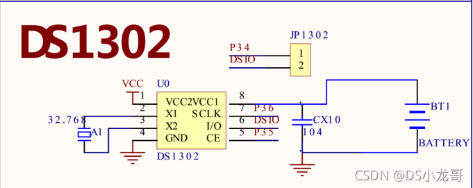
Figure 4-7-1
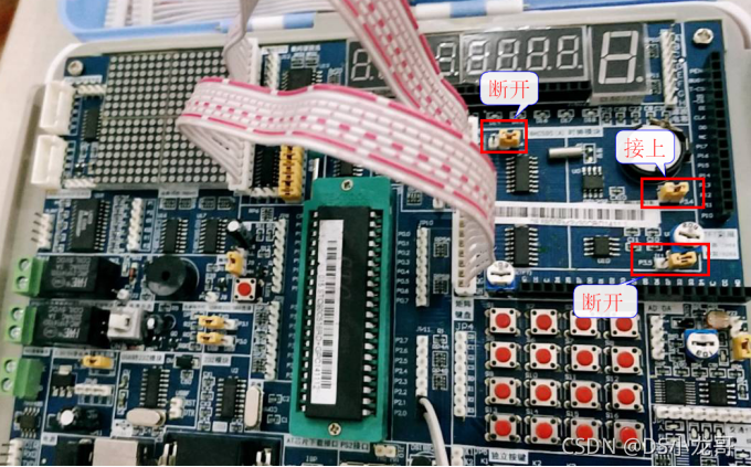
Figure 4-7-2
Before driving DS1302, disconnect JP595 jumper cap and J11 jumper cap on the test board. Connect JP1302 jumper cap.
4.7.2 introduction to DS1302 clock chip
There are many popular serial real-time clock (RTC) chips, such as DS1302, DS1307, PCF8485 and so on. These chips are widely used because of their simple interface, low price and convenient use.
The real-time clock chip introduced in this section is DS1302. It is a low-power real-time clock chip with trickle (small) current charging ability. It can time year, month, day, week, hour, minute and second, and has leap year compensation and other functions. DS1302 adopts serial data transmission, can provide programmable charging function for power failure protection power supply, and can turn off the charging function. The crystal oscillator adopts 32.768kHz.
DS1302 only needs three lines to communicate with MCU: (1) RST (reset), (2) I/O (data line) and (3) SCLK (serial clock); Data can be transmitted in single byte form of one byte at a time or multi byte form of up to 31 bytes.
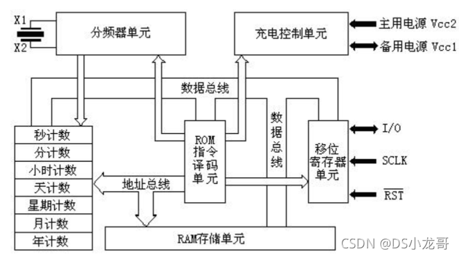
Figure 4-7-3 internal block diagram of DS1302
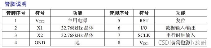
Figure 4-7-4 pin function description
4.7.3 introduction to sequence diagram
(1). Read data timing
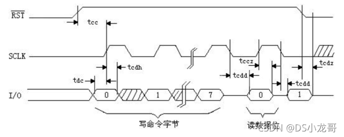
Figure 4-7-5
The above timing chart is the timing chart for reading data from DS1302 register. Before reading data, you need to set the register address of the read data, and then receive the data returned by DS1302.
It can be seen from the timing chart that before starting data transmission, RST remains low and the clock line remains low. When starting data transmission, RST remains high. The data is transmitted from the low position first, the data is changed at the rising edge, the data is kept stable at the falling edge, and the rst remains low after the data transmission is completed.
Example code:
/*
Function function: read a byte of data from the specified register of DS1302
*/
u8 DS1302_ReadByte(u8 addr)
{
    u8 n=0,dat=0;
    DS1302_RST=1;   //Then the DS1302_RST(CE) is set to high level.
    /*1. Set read address*/
    for(n=0;n<8;n++)
    {
        DS1302_IO=addr&0x01;//Data is transmitted from low bit
        addr>>=1;
        DS1302_SCLK=1;//When the data is on the rising edge, the DS1302 reads the data
        DS1302_SCLK=0;//When DS1302 falling edge, place data
    }
    /*2. Read data*/
    for(n=0;n<8;n++)
    {
        dat>>=1;
        if(DS1302_IO)dat|=0x80;
        DS1302_SCLK=1;
        DS1302_SCLK=0;//When DS1302 falling edge, place data
    }
    DS1302_RST=0;
    //Necessary operation, reset time
    DS1302_IO=0;
    DS1302_IO=1;
return dat;
}
(2). Write data timing
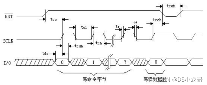
Figure 4-7-6
The above timing chart is the timing chart for writing data to the DS1302 register. Before writing data, you need to set the register address of the written data, and then write the actual data.
It can be seen from the timing chart that before starting data transmission, RST remains low and the clock line remains low. When starting data transmission, RST remains high. The data is transmitted from the low position first, the data is changed at the rising edge, the data is kept stable at the falling edge, and the rst remains low after the data transmission is completed.
Example code:
/*
Function: write a byte of data to the specified register of DS1302
*/
void DS1302_WriteByte(u8 addr,u8 dat)
{
    u8 n;
    DS1302_RST=1; //Then the DS1302_RST(CE) is set to high level.
    /*1. Set address to write*/
    for(n=0;n<8;n++)
    {
        DS1302_IO=addr&0x01;//Data is transmitted from low bit
        addr>>=1;
        DS1302_SCLK=1;//When the data is on the rising edge, the DS1302 reads the data
        DS1302_SCLK=0;
    }

    /*2. Write data*/
    for(n=0;n<8;n++)
    {
        DS1302_IO=dat&0x01;
        dat>>=1;
        DS1302_SCLK=1;//When the data is on the rising edge, the DS1302 reads the data
        DS1302_SCLK=0;
    }
    DS1302_RST=0;//End of data transfer
}
(3). Single byte read-write sequence diagram
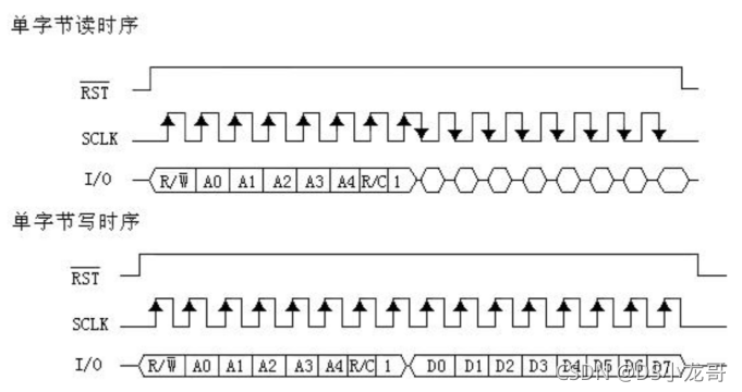
Figure 4-7-7
4.7.4 register definition
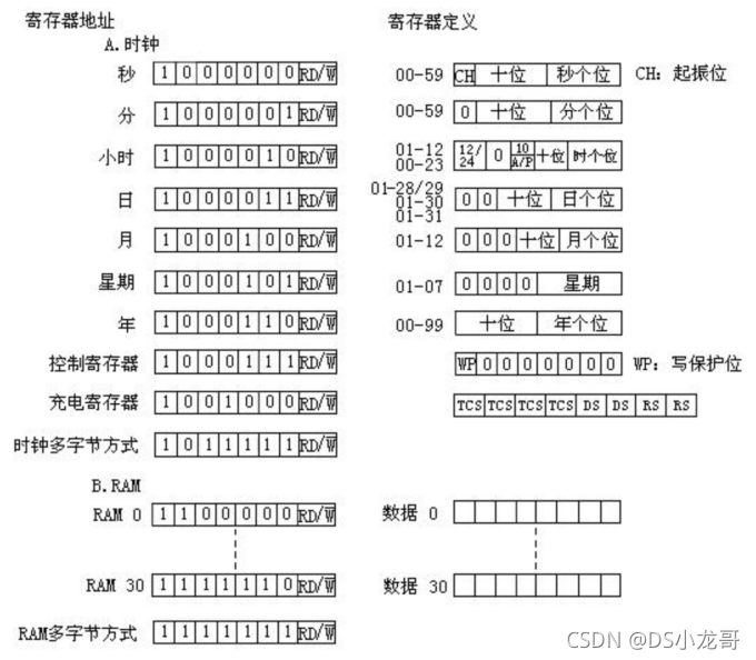
Figure 4-7-8
The lowest bit of the register is the read-write control bit, 0 is write and 1 is read.
The data in the register is in BCD code format, and the decimal system can be separated: ten bits are separated from data > > 4, and ten bits are obtained from data & 0x0f.
Second register description:
Bit 7 of the second register is defined as the clock pause bit. When this bit is set to logic 1, the clock oscillator stops and the DS1302 is put into a low-power backup mode, with a power consumption of less than 100 nanoamp s. When this bit is written as logic 0, the clock will start.
Control register description:
Bit 7 of the write protect register is the write protect bit. The start 7 bits (bits 0-6) are set to zero, and zero is always read out during the read operation. Bit 7 must be zero before writing to the clock or RAM. When it is high, the write protect bit prohibits writing to any other register.
Hour register description:
Bit 7 of the hour register is defined as the 12 or 24-hour mode selection bit. When it is high, select the 12 hour mode. In the 12 hour mode, bit 5 is the AM/PM bit, and this bit is the logic high level, indicating PM. In the 24-hour mode, bit 5 is the second 10 hour bit (20-23 hours).
The above register address is converted into hexadecimal address as follows:
Control register (write protect): (write) 0x8E
Year register address: (write) 0x8c (read) 0x8c|0x01
Month register address: (write) 0x88 (read) 0x88|0x01
Daily register address: (write) 0x86 (read) 0x86|0x01
Time register address: (write) 0x84 (read) 0x84|0x01
Sub register address: (write) 0x82 (read) 0x82|0x01
Second register address: (write) 0x80 (read) 0x80 × 0x01
Week register address: (write) 0x8a (read) 0x8a|0x01
4.7.5 detailed function introduction of register
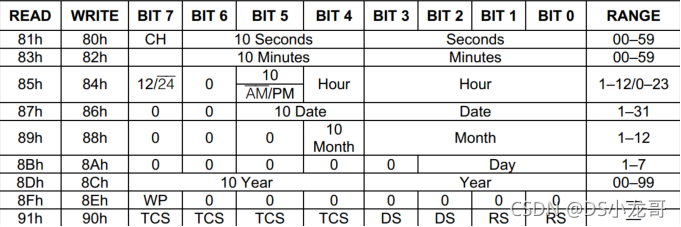
Fig. 4-7-9 register diagram
Register 0: the highest bit CH is a clock stop flag bit. If the clock circuit has a standby power supply, you can check this bit first after power on. If this bit is 0, it means that the clock chip continues to operate normally due to the supply of standby power supply after the system is powered off; If this bit is 1, it means that the clock chip does not work after the system is powered down. If Vcc1 is suspended or the battery is dead, when it is powered on again next time, read this bit, and this bit is 1. You can judge whether the clock still operates normally after the MCU system is powered off. The remaining 7 bits, the upper 3 bits are ten bits of the second, the lower 4 bits are one bit of the second, the DS1302 is internally BCD code, and the maximum ten bits of the second is 5.
Register 1: the highest bit is unused. Among the remaining 7 bits, the upper 3 bits are ten bits of the minute and the lower 4 bits are ten bits of the minute.
Register 2: bit7 represents 12-hour system and 0 represents 24-hour system; bit6 is fixed to 0, bit5 in the 12 hour system, 0 represents the morning and 1 represents the afternoon. In the 24-hour system, bit4 and bit4 represent the ten digits of the hour, and the lower four digits represent the one digit of the hour.
Register 3: the upper 2 bits are fixed to 0, bit5 and bit4 are ten bits of the date, and the lower 4 bits are one bit of the date.
Register 4: the upper 3 bits are fixed to 0, bit4 is the ten bits of the month, and the lower 4 bits are the one bits of the month.
Register 5: the upper 5 bits are fixed to 0, and the lower 3 bits represent week. (1~7)
Register 6: the upper 4 bits represent the ten bits of the year, and the lower 4 bits represent the one bit of the year. 00 ~ 99 refers to 2000 ~ 2099.
Register 7: the highest write protected bit. If this bit is 1, it is prohibited to write data to any other register or the 31 byte RAM. Therefore, this bit must be written as 0 before writing data.
4.7.6 BCD code to decimal
BCD code is a 4-bit binary number to represent the 10 numbers 0 ~ 9 in 1-bit decimal number. It is a binary digital coding form and a binary coded decimal code. BCD code uses four bits to store a decimal number, which makes the conversion between binary and decimal convenient.
Example code:
/*Function function: convert decimal data to BCD code*/
u8 DEC_TO_BCD(u8 val)
{
    return ((val/10)<<4)+val%10;
}
/*Function function: convert BCD code data to decimal format*/
u8 BCD_TO_DEC(u8 val)
{
return (val&0x0f)+(val>>4)*10;
}
4.7.7 DS1302 example code
The following code realizes the register reading and writing, time setting and reading of DS1302. Judge whether DS1302 works normally before in the main function. If DS1302 is in the stop timing state, reset the time. In the loop code, print the read time to the serial port every 1 second.
(description of hardware platform: CPU is STC90C516RD, crystal oscillator frequency is 12MHZ, working in 12T mode, and one machine cycle is 1us time)
Example code:
#include <reg51.h>
//Define the IO port used by ds1302
sbit DS1302_IO=P3^4;
sbit DS1302_RST=P3^5;
sbit DS1302_SCLK=P3^6;

u8 DS1302_TIME[7]; //Time for storing and reading

/*
Function function: convert decimal data to BCD code
*/
u8 DEC_TO_BCD(u8 val)
{
    return ((val/10)<<4)+val%10;
}

/*
Function function: convert BCD code data to decimal format
*/
u8 BCD_TO_DEC(u8 val)
{
    return (val&0x0f)+(val>>4)*10;
}

void DS1302_Init(void)
{
   DS1302_RST=0;
   DS1302_SCLK=0;//DS1302_SCLK is set to low level.
}

/*
Function: write a byte of data to the specified register of DS1302
*/
void DS1302_WriteByte(u8 addr,u8 dat)
{
    u8 n;
    DS1302_RST=1; //Then the DS1302_RST(CE) is set to high level.
    /*1. Set address to write*/
    for(n=0;n<8;n++)
    {
        DS1302_IO=addr&0x01;//Data is transmitted from low bit
        addr>>=1;
        DS1302_SCLK=1;//When the data is on the rising edge, the DS1302 reads the data
        DS1302_SCLK=0;
    }

    /*2. Write data*/
    for(n=0;n<8;n++)
    {
        DS1302_IO=dat&0x01;
        dat>>=1;
        DS1302_SCLK=1;//When the data is on the rising edge, the DS1302 reads the data
        DS1302_SCLK=0;
    }
    DS1302_RST=0;//End of data transfer
}

/*
Function function: read a byte of data from the specified register of DS1302
*/
u8 DS1302_ReadByte(u8 addr)
{
    u8 n=0,dat=0;
    DS1302_RST=1;   //Then the DS1302_RST(CE) is set to high level.
    /*1. Set read address*/
    for(n=0;n<8;n++)
    {
        DS1302_IO=addr&0x01;//Data is transmitted from low bit
        addr>>=1;
        DS1302_SCLK=1;//When the data is on the rising edge, the DS1302 reads the data
        DS1302_SCLK=0;//When DS1302 falling edge, place data
    }
    /*2. Read data*/
    for(n=0;n<8;n++)
    {
        dat>>=1;
        if(DS1302_IO)dat|=0x80;
        DS1302_SCLK=1;
        DS1302_SCLK=0;//When DS1302 falling edge, place data
    }
    DS1302_RST=0;
    //Necessary operation, reset time
    DS1302_IO=0;
    DS1302_IO=1;
    return dat;
}

/*
Function: set the time of DS1302 chip
DS1302 The time benchmark of starts from 2000. When setting the year, subtract 2000 and then enter the setting
 For example: DS1302_WriteTime(20,1,18,14,46,20,6);
*/
void DS1302_WriteTime(u8 year,u8 mon,u8 mday,u8 hour,u8 min,u8 sec,u8 week)
{
    DS1302_WriteByte(0x8E,0x00); //To disable write protection is to disable the write protection function
    DS1302_WriteByte(0x8c,DEC_TO_BCD(year)); //Set year
    DS1302_WriteByte(0x88,DEC_TO_BCD(mon));  //Set month
    DS1302_WriteByte(0x86,DEC_TO_BCD(mday)); //Set day
    DS1302_WriteByte(0x84,DEC_TO_BCD(hour)); //When setting
    DS1302_WriteByte(0x82,DEC_TO_BCD(min));  //Set score
    DS1302_WriteByte(0x80,DEC_TO_BCD(sec));  //Set seconds
    DS1302_WriteByte(0x8a,DEC_TO_BCD(week)); //Set week
    DS1302_WriteByte(0x8E,0x80);             //Turn on write protection
}

/*
Function: read the time of DS1302 clock
DS1302 The lowest bit of the register is the read / write bit, 0 is the write bit, and 1 is the read bit
*/
void DS1302_ReadTime(void)
{
    DS1302_TIME[0]=BCD_TO_DEC(DS1302_ReadByte(0x8c|0x01));//Read year
    DS1302_TIME[1]=BCD_TO_DEC(DS1302_ReadByte(0x88|0x01));//Read month
    DS1302_TIME[2]=BCD_TO_DEC(DS1302_ReadByte(0x86|0x01));//Read day
    DS1302_TIME[3]=BCD_TO_DEC(DS1302_ReadByte(0x84|0x01));//When reading
    DS1302_TIME[4]=BCD_TO_DEC(DS1302_ReadByte(0x82|0x01));//Read score
    DS1302_TIME[5]=BCD_TO_DEC(DS1302_ReadByte(0x80|0x01));//Read seconds
    DS1302_TIME[6]=BCD_TO_DEC(DS1302_ReadByte(0x8a|0x01));//Read week
}

int main()
{
    u8 stat;
    UART_Init();        //The baud rate of initialization serial port is 4800
    DS1302_Init();
    stat=DS1302_ReadByte(0x80|0x01);//Read seconds
    if(stat&0x80)
    {
        DS1302_WriteTime(2020-2000,1,18,16,33,33,6);
    }
    else
    {
        printf("DS1302 OK\r\n");
    }
    while(1)
    {
        DS1302_ReadTime();
        printf("DS1302:%d-%d-%d %d:%d:%d %d\r\n",
        (int)DS1302_TIME[0]+2000,
        (int)DS1302_TIME[1],
        (int)DS1302_TIME[2],
        (int)DS1302_TIME[3],
        (int)DS1302_TIME[4],
        (int)DS1302_TIME[5],
        (int)DS1302_TIME[6]
        );
        DelayMs(1000);
    }
}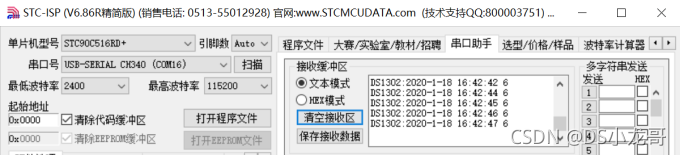
Figure 4-7-10