1, System clock
1. Clock tree
1. The system main frequency of mx6u is 528MHz, but by default, the internal boot rom will set the main frequency of I.MX6U to 396MHz
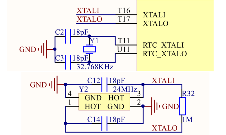
1. The system clock of mx6u-alpha development board comes from two parts: 32.768KHz crystal oscillator and 24MHz crystal oscillator. The 32.768KHz crystal oscillator is the RTC clock source of I.MX6U, and the 24MHz crystal oscillator is the clock source of I.MX6U core and other peripherals
Clock tree:
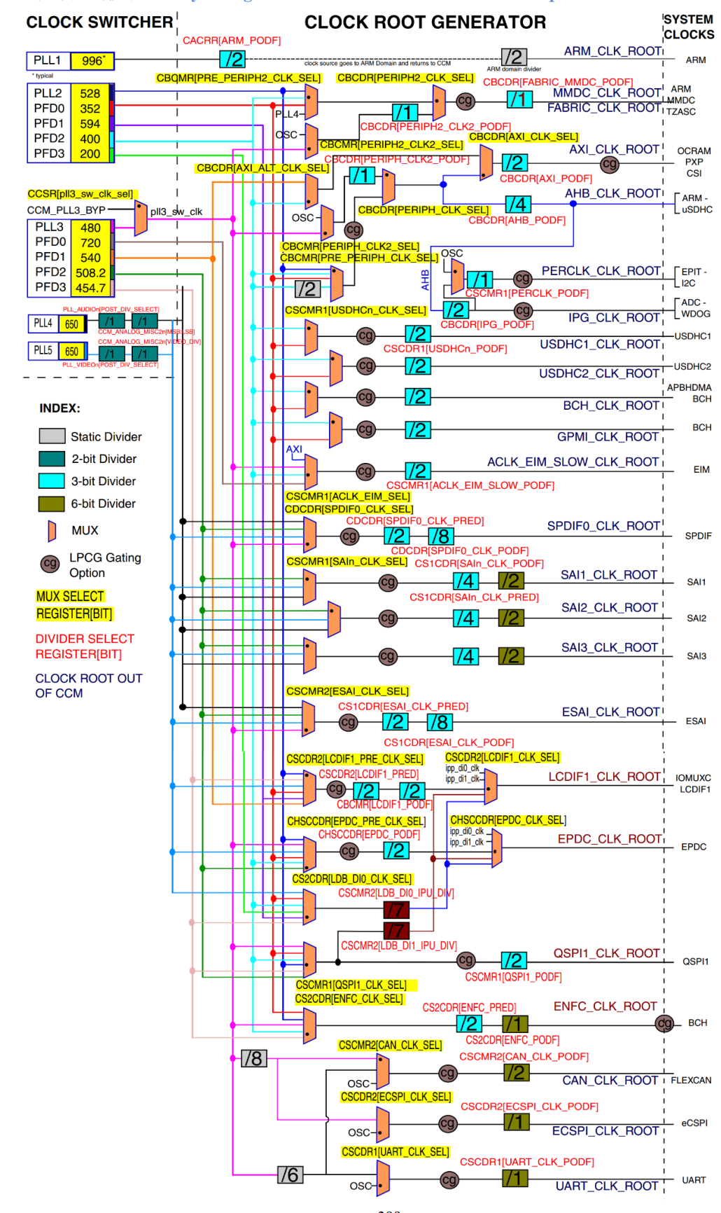
The clock tree has three parts: CLOCK_SWITCHER, CLOCK ROOT GENERATOR and SYSTEM CLOCKS. CLOCK_SWITCHER is 7-way PLL and 8-way PFD, and SYSTEM CLOCKS is the clock of chip peripherals. CLOCK ROOT GENERATOR selects the appropriate clock source from 7-way PLL and 8-way PFD and divides the frequency to peripherals for use.
Note: each line with different colors in the middle indicates that it comes from different clock sources. Combined with the annotation analysis of the icon on the left, for example, the yellow flag indicates the bit setting of the clock source register, and the red flag indicates the bit setting of the clock source frequency division coefficient register.
In order to facilitate clock generation, alpha generates 7-channel PLL from 24MHz crystal oscillator. PLL2 and PLL3 generate 4-way PDF0-3.
ARM_PLL(PLL1): it is used by the arm core. The arm core clock is generated by this PLL. This PLL can double the frequency up to 1.3GHz by programming
528_PLL(PLL2): also called System_PLL and pll2 are fixed 22 octave frequency. PLL2 =24MHz * 22 = 528MHz. Pll2 is divided into four PFDs: PLL2_PFD0~PLL2_PFD3. This 4-way PFD and 528_PLL
It serves as the clock source of the internal system bus and the root clock source of many other peripherals
USB1_PLL(PLL3): mainly used for USBPHY. PLL3 is a fixed 20 times frequency division, USB1_PLL=24MHz *20=480MHz
AUDIO_PLL(PLL4): used for audio related peripherals
VIDEO_PLL(PLL5): used to display related peripherals
ENET_PLL(PLL6): used to generate the clock required by the network. PLL6 is fixed as 20 + 5 / 6 octave, ENET_PLL=24MHz * (20+5/6)= 500MHz
USB2_PLL(PLL7): for USB2PHY, PLL7 is fixed to 20 octave, so PLL7=480MHz
Clock tree configuration peripheral clock: (ESAI peripheral as an example)
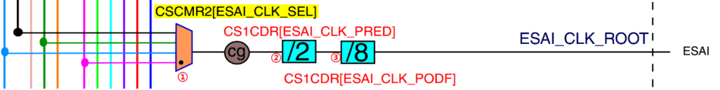
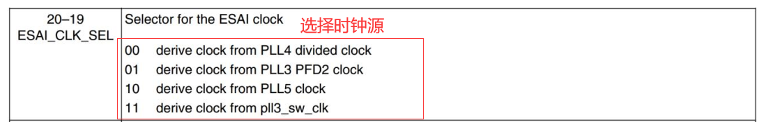
(1) this is the clock source selector. There are four optional clock sources: PLL4, PLL5 and PLL3_PFD2 and pll3_sw_clk . Which channel is selected as the clock source of ESAI is determined by the ESAI of register CCM - > cscmr2_ CLK_ Determined by sel bit (yellow mark right above)
(2) Clock frequency divider, the frequency division value is determined by the register CCM_ Esai of cs1cdr_ CLK_ Determined by PRED, 1 ~ 8 frequency division can be set (light blue is the 3bit distributor, icon)
(3) The same function as 2, Esai is obtained after twice frequency division_ CLK_ Root peripheral clock source
2. Kernel clock
Purpose: set the ARM core clock to 528Mhz
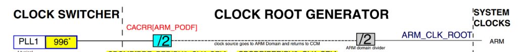
(1) The core clock source comes from PLL1, and then the system clock is obtained by two frequency division (the gray frequency divider behind is static divider, which does not divide the frequency). Therefore, to set the system clock to 528MHz, it is necessary to modify the value of PLL1 to 528 * 2 = 1056mhz < 1.3GHz, and the frequency of PLL1 passes through the register CCM_ANALOG_PLL_ARMn to set
CCM_CACRR register (frequency division)
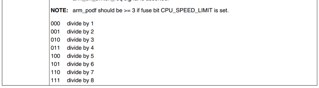
ARM_ Only the third bit is used in podf. Set it to 2 frequency division and write 1 to the register
CCM_ ANALOG_ PLL_ Armn (frequency)
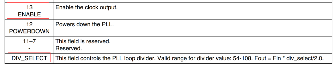
13 bits: clock output enable, 1: enable PLL1 output; 0: turn off PLL1 output
DIV_SELECT: set the output frequency of PLL1, PLL1 CLK = Fin *div_seclec/2.0, Fin=24MHz
Writable range: 54 ~ 108, so PLL1 needs to output 1056MHz, div_select to be set to 88
(2) however, when modifying the PLL1 clock frequency, it is necessary to change the core clock source to another clock source first, because PLL1 is generally selected as the time base by default, and the clock must provide the time base to the system during modification.
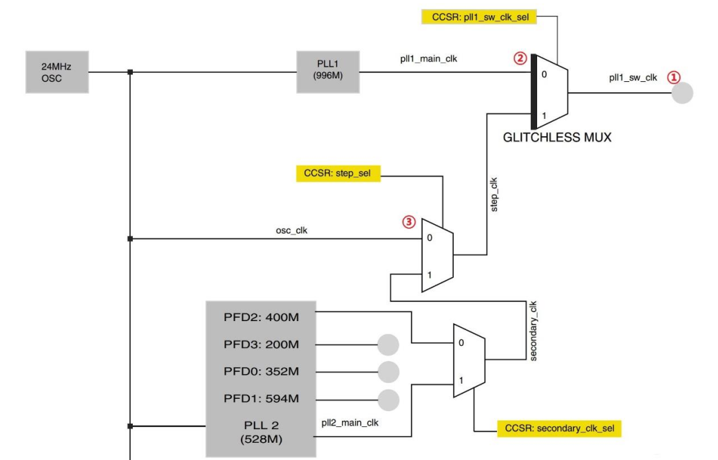
pll1_sw_clk is the output frequency of PLL1. Clock source: pll1_main_clk and step_clk, by register CCM_ PLL1 of CCSR_ SW_ CLK_ SEL bit decision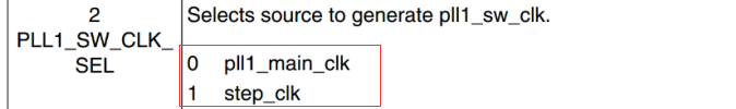
And step_ The clock source of CLK can come from osc_clk and secondary_clk, usually osc_clk(24MHz crystal oscillator), controlled by register CCM_CCSR STEP_SEL bit decision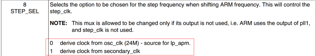
/* 1.1,Judge whether the current ARM kernel is started by the clock source used. Under normal circumstances, the ARM kernel is started by pll1_sw_clk driven, and
	 *      pll1_sw_clk There are two sources: pll1_main_clk and tep_clk.
	 *      If we want to make the ARM kernel run to 528M, we must choose pll1_main_clk is used as the clock source of pll1.
	 *      If we want to modify PLL1_ main_ For CLK clock, PLL1 must be set first_ sw_ CLK from pll1_main_clk switch to step_clk,
	 *		When PLL1 is modified_ main_ After CLK, pll1_sw_clk switches back to pll1_main_clk.  And step_clk clock source can be selected
	 * 		24MHz crystal oscillator on the board.
	 */

	if((((CCM->CCSR) >> 2) & 0x1 ) == 0) 	/* Current PLL1_ sw_ PLL1 used by CLK_ main_ clk*/
	{
		CCM->CCSR &= ~(1 << 8);				/* Configure step_clk clock source is 24MH OSC */
		CCM->CCSR |= (1 << 2);				/* Configure pll1_sw_clk clock source is step_clk */
	}

	/* 1.2,Set pll1_main_clk is 528MHz
	 *      Because pll1_sw_clk will be divided by two when it enters the ARM core!
	 *      Configure CCM_ ANLOG->PLL_ Arm register
	 *      bit13: 1 Enable clock output
	 *      bit[6:0]: 88, By formula: Fout = Fin * div_select / 2.0,528=24*div_select/2.0,
	 *              		Get: div_select=    88
	 */
	CCM_ANALOG->PLL_ARM = (1 << 13) | ((88 << 0) & 0X7F); 	/* Configure pll1_main_clk=528MHz */
	CCM->CCSR &= ~(1 << 2);									/* pll_sw_clk clock switches back to pll1_main_clk */
	CCM->CACRR = 1;											/* ARM The kernel clock is pll1_sw_clk=1056/2=528Mhz */
First judge the clock source used by the ARM kernel, and then set the step of the register CCSR_ SEL bit, set step_ The clock source of CLK is a 24M crystal oscillator, and then set the PLL1 of register CCSR_ SW_ CLK_ SEL bit, set PLL1_ sw_ The clock source of CLK is step_clk=24MHz, set the main frequency of I.MX6U to 24MHz, which comes directly from the external 24M crystal oscillator
After the clock source is modified, the frequency of PLL1 can be modified to 1056MHz and CCM_ ANALOG_ PLL_ The lower 6 bits of armn can be written to 88 and 13 bits can be enabled. Set PLL1 of register CCSR_ SW_ CLK_ SEL bit, reset PLL1_ sw_ The clock source of CLK is switched back to pll1_main_clk, PLL1 after switching back_ sw_ CLK is equal to 1056MHz. Finally, set the register CCM_CACRR arm_ The podf is divided into two frequencies, and the core dominant frequency of MX6U is 1056/2=528MHz
3.FPD clock
After setting the system clock, other PLL and PFD clocks should be set, mainly the 4-way PFD of PLL2 and PLL3
8-channel FPD frequency meter:

Set the 4-channel PFD frequency of PLL2, and the register used is CCM_ANALOG_PFD_528n
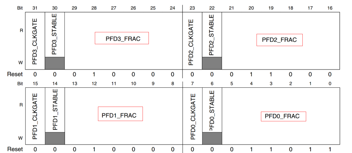
It is just divided into four groups with 8 bit s in each group, corresponding to PFD0~PFD3 and pfdx respectively_ FRAC: PLL2_ Frequency division number of pfdx #
Frequency calculation formula: PLL2_PFDx = 528*18/PFDx_FRAC
To set pll2_ If the frequency of pfd0 is 352MHz, then PFD0_FRAC=528*18/352=27, the same for others.
Set the frequency of 4-way PFD of PLL3, and the register used is CCM_ANALOG_PFD_480n
Frequency calculation formula: PLL3_PFDX=480*18/PFDX_FRAC(X=0~3) is the same except that the formula is different.
uint8_t reg = 0;

/* 2,Set each PFD of PLL2(SYS PLL) */
reg = CCM_ANALOG->PFD_528;
reg &= ~(0X3F3F3F3F);		/* Clear original settings 						*/
reg |= 32<<24;				/* PLL2_PFD3=528*18/32=297Mhz 	*/
reg |= 24<<16;				/* PLL2_PFD2=528*18/24=396Mhz(DDR Clock used, maximum 400Mhz) */
reg |= 16<<8;				/* PLL2_PFD1=528*18/16=594Mhz 	*/
reg |= 27<<0;				/* PLL2_PFD0=528*18/27=352Mhz  	*/
CCM_ANALOG->PFD_528=reg;	/* Set PLL2_PFD0~3 		 		*/

/* 3,Set each PFD of PLL3(USB1) */
reg = 0;					/* Clear   */
reg = CCM_ANALOG->PFD_480;
reg &= ~(0X3F3F3F3F);		/* Clear original settings 							*/
reg |= 19<<24;				/* PLL3_PFD3=480*18/19=454.74Mhz 	*/
reg |= 17<<16;				/* PLL3_PFD2=480*18/17=508.24Mhz 	*/
reg |= 16<<8;				/* PLL3_PFD1=480*18/16=540Mhz		*/
reg |= 12<<0;				/* PLL3_PFD0=480*18/12=720Mhz	 	*/
CCM_ANALOG->PFD_480=reg;	/* Set PLL3_PFD0~3 					*/
Tip: set 8-13 to 16, and the remaining bits are not affected
GPIO - > Dr & = ~ (0X00003F00) / * clear the corresponding bit to 0*/
GPIO - > Dr | = 16 < < 8 / * write 16 from bit 8*/
4.AHB, IPG, PERCLK clock
After 7-way PLL and 8-way PFD are set, AHB needs to be set_ CLK_ Root and IPG_CLK_ROOT clock
Peripheral root clock frequency table:
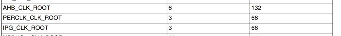
Transfer AHB_CLK_ROOT,IPG_CLK_ROOT and PERCLK_CLK_ROOT is set to 132MHz, 66MHz and 66MHz respectively
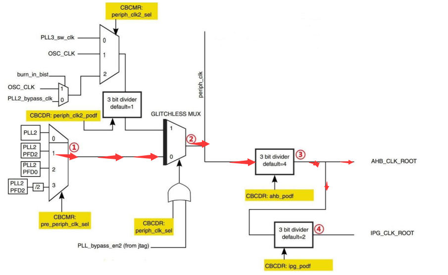
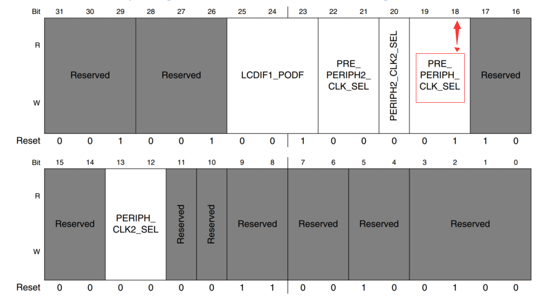
(1) Select pre first_ periph_ CLK clock source, pll2 and pll2 can be selected_ PFD2, PLL2_PFD0 and PLL2_PFD2/2. Register CCM_ Pre of cbcmr_ PERIPH_ CLK_ The SEL bit determines which one to select, and pll2 is selected by default_ PFD2,pre_periph_clk=PLL2_PFD2=396MHz

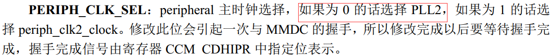
(2) Select periph_ The clock source of CLK is controlled by the register CCM_ Periph of cbcdr_ CLK_ SEL bit and PLL_bypass_en2 consists of or to choose from. When CCM_ Periph of cbcdr_ CLK_ Periph when sel bit is 0_ clk=pr_ periph_clk=396MHz
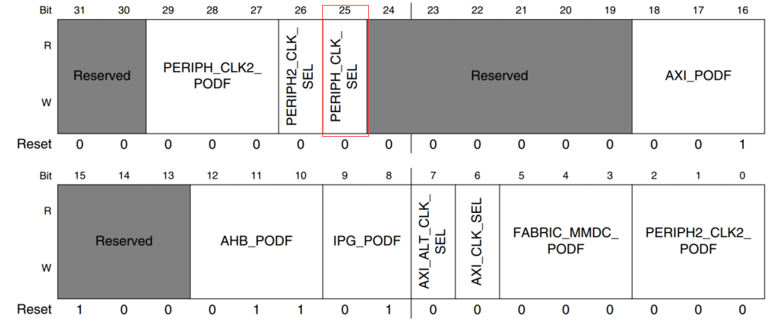
(3) Set AHB_ CLK_ The frequency division value of root is determined by the AHB of CBCDR_ Determined by podf bit, 1 ~ 8 frequency division can be set if AHB is desired_ CLK_ If root = 132mhz, it should be set to 3 frequency division: 396/3=132MHz. Although the default frequency division is 4, the internal boot rom of MX6U changes it to 3
(4) Set IPG_ CLK_ Frequency division value of root, IPG_ CLK_ The root clock source is AHB_CLK_ROOT, if you want to IPG_ CLK_ If root = 66MHz, you should set 2 frequency division: 132/2=66MHz

(5) Set PERCLK_CLK_ROOT clock frequency
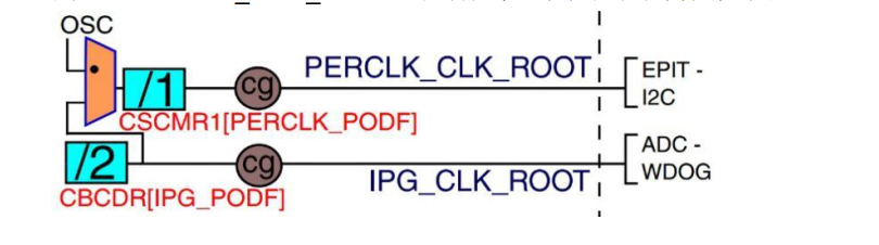
PERCLK_ CLK_ There are two sources of root: OSC(24MHz) and IPG_CLK_ROOT, by register CCM_ Perclk of cscmr1_ CLK_ SEL bit. If perclk is selected for 0_ CLK_ The clock source of root is IPG_CLK_ROOT=66MHz . You can register CCM_ Perclk of cscmr1_ Podf bit to set frequency division. If perclk is to be set_ CLK_ If the root is 66MHz, it should be set to 1 frequency division
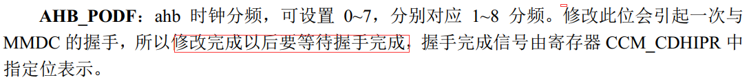
Note: when modifying the following clock selector or frequency divider, handshake with MMDC will occur
mmdc_podf
periph_clk_sel
periph2_clk_sel
arm_podf
ahb_podf
After the handshake signal occurs, you need to wait for the handshake to complete and register CCM_CDHIPR stores whether the handshake signal is completed. If the corresponding bit is 1, it means that the handshake is not completed. If it is 0, it means that the handshake is completed.
	/* 4,Set the minimum 6Mhz and maximum 132mhz of AHB clock (boot ROM can be set automatically without setting)*/
	CCM->CBCMR &= ~(3 << 18); 	/* Clear settings*/
	CCM->CBCMR |= (1 << 18);	/* pre_periph_clk=PLL2_PFD2=396MHz */
	CCM->CBCDR &= ~(1 << 25);	/* periph_clk=pre_periph_clk=396MHz */
	while(CCM->CDHIPR & (1 << 5));/* Wait for the handshake to complete */

	/* Modify AHB_ When the podf bit is, it is necessary to disable the AHB first_ CLK_ Root output, but
	 * Closed AHB not found_ CLK_ Root output register, so it cannot be set.
	 * Set AHB below_ The code of podf is only for learning reference and can not be used directly!!
	 * Internal boot rom will AHB_PODF is set to 3 frequency division, even if we do not set AHB_PODF,
	 * AHB_ROOT_CLK It is still equal to 396/3=132Mhz.
	 */
#if 0
	/* To close AHB first_ ROOT_ CLK output, otherwise the clock setting will be wrong */
	CCM->CBCDR &= ~(7 << 10);	/* CBCDR AHB of_ Podf reset */
	CCM->CBCDR |= 2 << 10;		/* AHB_PODF 3 Frequency division, AHB_CLK_ROOT=132MHz */
	while(CCM->CDHIPR & (1 << 1));/* Wait for the handshake to complete */
#endif

	/* 5,Set IPG_ CLK_ The minimum root is 3Mhz and the maximum root is 66Mhz (boot rom can be set automatically without setting)*/
	CCM->CBCDR &= ~(3 << 8);	/* CBCDR IPG for_ Podf reset */
	CCM->CBCDR |= 1 << 8;		/* IPG_PODF 2 Frequency division, IPG_CLK_ROOT=66MHz */

	/* 6,Set PERCLK_CLK_ROOT clock */
	CCM->CSCMR1 &= ~(1 << 6);	/* PERCLK_CLK_ROOT The clock source is IPG */
	CCM->CSCMR1 &= ~(7 << 0);	/* PERCLK_PODF Bit reset, i.e. 1 Frequency Division */
2, Clock initial code
/*
 * @description	: Initialize the system clock, set the system clock to 792Mhz, and set each of PLL2 and PLL3
 				  PFD Clock, all clock frequencies are in accordance with the values recommended in the official Manual of I.MX6U
 * @param 		: nothing
 * @return 		: nothing
 */
void imx6u_clkinit(void)
{
	unsigned int reg = 0;
	/* 1.1,Judge whether the current ARM kernel is started by the clock source used. Under normal circumstances, the ARM kernel is started by pll1_sw_clk driven, and
	 *      pll1_sw_clk There are two sources: pll1_main_clk and tep_clk.
	 *      If we want to make the ARM kernel run to 528M, we must choose pll1_main_clk is used as the clock source of pll1.
	 *      If we want to modify PLL1_ main_ For CLK clock, PLL1 must be set first_ sw_ CLK from pll1_main_clk switch to step_clk,
	 *		When PLL1 is modified_ main_ After CLK, pll1_sw_clk switches back to pll1_main_clk.  And step_clk clock source can be selected
	 * 		24MHz crystal oscillator on the board.
	 */

	if((((CCM->CCSR) >> 2) & 0x1 ) == 0) 	/* Current PLL1_ sw_ PLL1 used by CLK_ main_ clk*/
	{
		CCM->CCSR &= ~(1 << 8);				/* Configure step_clk clock source is 24MH OSC */
		CCM->CCSR |= (1 << 2);				/* Configure pll1_sw_clk clock source is step_clk */
	}

	/* 1.2,Set pll1_main_clk is 528MHz
	 *      Because pll1_sw_clk will be divided by two when it enters the ARM core!
	 *      Configure CCM_ ANLOG->PLL_ Arm register
	 *      bit13: 1 Enable clock output
	 *      bit[6:0]: 88, By formula: Fout = Fin * div_select / 2.0,528=24*div_select/2.0,
	 *              		Get: div_select=    88
	 */
	CCM_ANALOG->PLL_ARM = (1 << 13) | ((88 << 0) & 0X7F); 	/* Configure pll1_main_clk=528MHz */
	CCM->CCSR &= ~(1 << 2);									/* pll_sw_clk clock switches back to pll1_main_clk */
	CCM->CACRR = 1;											/* ARM The kernel clock is pll1_sw_clk=1056/2=528Mhz */

	/* 2,Set each PFD of PLL2(SYS PLL) */
	reg = CCM_ANALOG->PFD_528;
	reg &= ~(0X3F3F3F3F);		/* Clear original settings 						*/
	reg |= 32<<24;				/* PLL2_PFD3=528*18/32=297Mhz 	*/
	reg |= 24<<16;				/* PLL2_PFD2=528*18/24=396Mhz(DDR Clock used, maximum 400Mhz) */
	reg |= 16<<8;				/* PLL2_PFD1=528*18/16=594Mhz 	*/
	reg |= 27<<0;				/* PLL2_PFD0=528*18/27=352Mhz  	*/
	CCM_ANALOG->PFD_528=reg;	/* Set PLL2_PFD0~3 		 		*/

	/* 3,Set each PFD of PLL3(USB1) */
	reg = 0;					/* Clear   */
	reg = CCM_ANALOG->PFD_480;
	reg &= ~(0X3F3F3F3F);		/* Clear original settings 							*/
	reg |= 19<<24;				/* PLL3_PFD3=480*18/19=454.74Mhz 	*/
	reg |= 17<<16;				/* PLL3_PFD2=480*18/17=508.24Mhz 	*/
	reg |= 16<<8;				/* PLL3_PFD1=480*18/16=540Mhz		*/
	reg |= 12<<0;				/* PLL3_PFD0=480*18/12=720Mhz	 	*/
	CCM_ANALOG->PFD_480=reg;	/* Set PLL3_PFD0~3 					*/

	/* 4,Set the minimum 6Mhz and maximum 132mhz of AHB clock (boot ROM can be set automatically without setting)*/
	CCM->CBCMR &= ~(3 << 18); 	/* Clear settings*/
	CCM->CBCMR |= (1 << 18);	/* pre_periph_clk=PLL2_PFD2=396MHz */
	CCM->CBCDR &= ~(1 << 25);	/* periph_clk=pre_periph_clk=396MHz */
	while(CCM->CDHIPR & (1 << 5));/* Wait for the handshake to complete */

	/* Modify AHB_ When the podf bit is, it is necessary to disable the AHB first_ CLK_ Root output, but
	 * Closed AHB not found_ CLK_ Root output register, so it cannot be set.
	 * Set AHB below_ The code of podf is only for learning reference and can not be used directly!!
	 * Internal boot rom will AHB_PODF is set to 3 frequency division, even if we do not set AHB_PODF,
	 * AHB_ROOT_CLK It is still equal to 396/3=132Mhz.
	 */
#if 0
	/* To close AHB first_ ROOT_ CLK output, otherwise the clock setting will be wrong */
	CCM->CBCDR &= ~(7 << 10);	/* CBCDR AHB of_ Podf reset */
	CCM->CBCDR |= 2 << 10;		/* AHB_PODF 3 Frequency division, AHB_CLK_ROOT=132MHz */
	while(CCM->CDHIPR & (1 << 1));/
* Wait for the handshake to complete */
#endif

	/* 5,Set IPG_ CLK_ The minimum root is 3Mhz and the maximum root is 66Mhz (boot rom can be set automatically without setting)*/
	CCM->CBCDR &= ~(3 << 8);	/* CBCDR IPG for_ Podf reset */
	CCM->CBCDR |= 1 << 8;		/* IPG_PODF 2 Frequency division, IPG_CLK_ROOT=66MHz */

	/* 6,Set PERCLK_CLK_ROOT clock */
	CCM->CSCMR1 &= ~(1 << 6);	/* PERCLK_CLK_ROOT The clock source is IPG */
	CCM->CSCMR1 &= ~(7 << 0);	/* PERCLK_PODF Bit reset, i.e. 1 Frequency Division */
}