Introduction
_Previously, the design was done on Xilinx's field bus, but only the AXI interface was known, but the protocol was not fully understood. Now it is necessary to design the whole system with AXI bus, so it is necessary to know this protocol in detail.
Reference material
IHI0022H: AMBA AXI and ACE Protocol Specification
IHI0051A: AMBA 4 AXI4-Stream Protocol Specification
_Both of the above are official ARM documents, which can be found in ARM's Official Network Found, these two documents describe AXI4, AXI4-Lite, and AXI4-Stream in detail. In addition to these two documents, there are also several IP documents for Xilinx, including AXI Interconnect, SmartConnect, AXI4-Stream Interconnect, which just need a general look.
_There are also many posts on the Internet about the AXI protocol, which are also well written and detailed. This article will be less, as it is only a few notes I have taken during the reading process. If you really want to know these, it is strongly recommended that you read the two Specification s above with your heart!
AXI Protocol
- Characteristic
- Separate Address, Control and Data Control
- Supports misaligned data transfer
- Support Burst Transport
- Read-Write Channel Separation
- Supports Unordered Transport
- AXI structure
- There are five independent channels: AR, R, AW, W and B, which correspond to read address, read data, write address, write data and write response.
- Address channel with control information
- B is the response channel to return the write response
- R-channel has not only read data but also response information
- Public address and data bus when bus is interconnected; Or public address lines, multiple data buses; Or you have multiple addresses and data buses.
- Global signal
- Clock, rising edge sampling; Reset Low Level Effective
- Clock and Reset
- Clock rise is valid, signals between interfaces have no combined logic path
- Reset can be asynchronous but must be released synchronously
- When resetting, the VALID signals of AW, AR and W channels at the manager end should be low. The VALID signal of R and B channels at subordinate end should be low
- VALID becomes valid only after resetting the first clock rising edge after undo
- VALID signals of the same channel cannot depend on READY signals
- Only READY can be undone after VALID is valid
- destination can wait for VALID to appear before generating READY
- After READY, you can undo it before VALID appears
- Channel signal
- It is recommended that AWREADY and ARREEADY default to high level, which can be faster
- WDATA RDATA recommended for inactive byte lanes is low level
- The relationship between channels
- Write response is generated after the LAST signal for write data is valid
- Read data to send data after the read address is sent to subordinate
- These two sets of relationships are defined in the agreement, which means there may be situations where writing data comes first or then writing addresses, which are allowed.
- Transaction structure
- The AXI protocol is based on burst transmission, which is computed by subordinate because manager sends only one starting address and the subsequent byte addresses are computed by subordinate.
- Can't exceed 4kB address boundary
- AxBurst defines the type of burst that cannot be terminated
- There are three types of bursts, INCR, FIXED, WRAP. INCR is self-additive, FIXED is fixed, WRAP rolls back the address, which is similar to INCR, but if the address reaches the upper boundary during transmission, it will bring the address back to the lower boundary.
- AxLEN represents the length of the burst, which is the number of VALID and READY handshakes that occur at a burst; AxSize represents the number of bytes transferred at a time, which is the number of bytes transferred at a handshake between VALID and READY.
- WRAP burst length can not exceed 16, INCR can exceed, but it is actually converted into multiple 16-length bursts
- AxSize is represented by 3bit, up to 128 bytes
- Regular Transaction General Transactions
- Regular_Transactions_Only This property is only supported for regular transactions if it is TRUE
- AxLen 1,2,4,8,16
- if AxLen > 1 , AxSize = data bus width
- AxBurst = INCR or WRAP, no FIXED
- Addresses are aligned
- Structure of data read and write
- Implement read-write and non-aligned transfers of mixed size data (because bytes are selected, data is transmitted in bytes, no size issues, mixed size data transfers can be achieved)
- byte strobe keeps low when the VALID signal is low or unchanges before
- narrow transfers is strobe strobe. In INCR and WRAP modes, the byte positions are different between different transmission times. In FIXED mode, the byte position is fixed.
- Two ways of misaligned transmission:
- Directly to an unaligned address, starting from this unaligned address to an aligned boundary counts as a transfer
- Use a lower aligned address and strobe to select
- One burst corresponds to one response, with four responses OKAY, EXOKAY, SLVERR, DECERR
- AxCHACHE
- subordinate devices are divided into peripheral and memory
- peripheral signal can be simplified because it implements fewer functions
- modifiable:
- A transaction can be split into multiple transactions
- Multiple transactions can be merged into one transaction
- A read transaction can read more data than it needs
- A write transaction can access more address space than it needs, strobe-checked
- In a separate generated transaction, AxADDR AxSIZE AxLEN AxBUREST can be overridden
- AxLOCK and AxPROT cannot be overridden
- With an ID you can have multiple Outstanding transactions
- RID corresponds to ARID
- Subordinate wants to sort RID s at a depth given when subordinate is designed. manager can't get this depth
- Connect prefaces each master's ID with the master's ID, so don't worry about duplicating IDs for different masters
- exclusive access: access to other master s is not supported
AXI4-Lite
- AxLEN for all transactions is 1
- Sizes are 32/64 data bitwidth
- exclusive access is not supported
- non-modifiable
- Although multiple Outstanding transactions are supported, subordinate can reasonably limit this by using handshake signals
AXI4-Stream
- Three byte types
- Data byte: Data
- Position byte:placeholder, does not contain data
- Null byte: Does not contain any data and location information
- Term Definition:
- Transfer: A handshake between VALID and READY
- Packet: Multiple Transfer s
- Frame: Multiple Packet s
- Four data streams
- Byte stream:data byte and null byte intervals
- data byte-only aligned transmission
- Continuous data byte s, with position byte s appended at the beginning and end to form an aligned transport
- Sparse stream:data byte and position byte intervals
- signal
- TSTRB and TKEEP:TSTRB distinguish data from position byte, TKEEP invalid is null byte
- Clock and Reset Same as AXI4
- The recommended number of bit s for tuser is an integer multiple of the number of bytes
- Different from AXI4
- AXI4 does not allow interleaving
- AXI4 has no maximum burst length
- Arbitrary data bit width for AXI4-Stream
- AXI4-Stream contains TID and TDEST source and destination information
- AXI4-Stream is more operational in defining TUSER
- AXI4-Stream has more TKEEP signals
Create custom AXI4-Lite peripherals
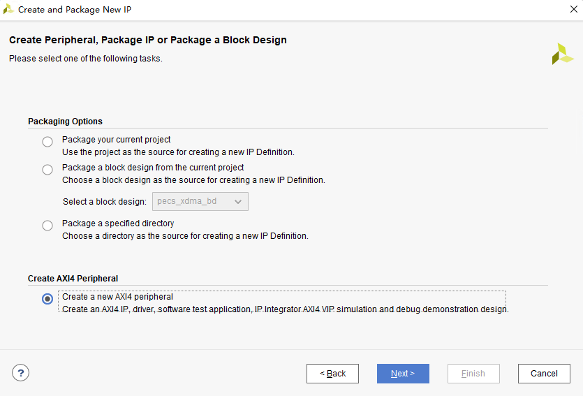
Under Vivado's Tool tag, there is an option called Create and Package New IPs. After clicking in, you can choose to create a new AXI4 peripheral and give it a name. You can put it in the IP library, call it in Block Design er, and right-click Edit in IP Packager.
_After clicking "Edit in IP Packager", you can see the top-level file of this IP and a module of its instantiated AXI4-Lite interface. We can incorporate our own design into this module, where most of the code generated initially does not need to be altered, and the comments are well written, with comments for each always block.
// Implement axi_awready generation
// axi_awready is asserted for one S_AXI_ACLK clock cycle when both
// S_AXI_AWVALID and S_AXI_WVALID are asserted. axi_awready is
// de-asserted when reset is low.
always @( posedge S_AXI_ACLK ) begin
	if ( S_AXI_ARESETN == 1'b0 ) begin
		axi_awready <= 1'b0;
		aw_en <= 1'b1;
	end
  	else begin
      	if (~axi_awready && S_AXI_AWVALID && S_AXI_WVALID && aw_en) begin
          // slave is ready to accept write address when
          // there is a valid write address and write data
          // on the write address and data bus. This design
          // expects no outstanding transactions.
          axi_awready <= 1'b1;
          aw_en <= 1'b0;
        end
        else if (S_AXI_BREADY && axi_bvalid) begin
              aw_en <= 1'b1;
              axi_awready <= 1'b0;
        end
      	else begin
          axi_awready <= 1'b0;
        end
    end
end
_The first always block is for awread and aw_en controls, and the comment also writes it "excepts no outstanding transactions", meaning that it can only process transactions one by one and receive new write data only after the response is complete. W ready is the same as awread, it gets aw_en control, only aw_ When en is high, it is possible for the two readies to be one; Then aw_en will only go up after the response is complete.
// Implement memory mapped register select and write logic generation
// The write data is accepted and written to memory mapped registers when
// axi_awready, S_AXI_AWVALID, axi_wready and S_AXI_WVALID are asserted. Write strobes are used to
// select byte enables of slave registers while writing.
// These registers are cleared when reset (active low) is applied.
// Slave register write enable is asserted when valid address and data are available
// and the slave is ready to accept the write address and write data.

assign slv_reg_wren = axi_wready && S_AXI_WVALID && axi_awready && S_AXI_AWVALID;

always @( posedge S_AXI_ACLK )
begin
  	if ( S_AXI_ARESETN == 1'b0 ) begin
		slv_reg0 <= 0;
		slv_reg1 <= 0;
		slv_reg2 <= 0;
		slv_reg3 <= 0;
    end
  	else begin
		if (slv_reg_wren) begin
			case ( axi_awaddr[ADDR_LSB+OPT_MEM_ADDR_BITS:ADDR_LSB] )
				2'h0:
					for ( byte_index = 0; byte_index <= (C_S_AXI_DATA_WIDTH/8)-1; byte_index = byte_index+1 )
						if ( S_AXI_WSTRB[byte_index] == 1 ) begin
						// Respective byte enables are asserted as per write strobes
						// Slave register 0
						slv_reg0[(byte_index*8) +: 8] <= S_AXI_WDATA[(byte_index*8) +: 8];
					end
				2'h1:
					for ( byte_index = 0; byte_index <= (C_S_AXI_DATA_WIDTH/8)-1; byte_index = byte_index+1 )
						if ( S_AXI_WSTRB[byte_index] == 1 ) begin
						// Respective byte enables are asserted as per write strobes
						// Slave register 1
						slv_reg1[(byte_index*8) +: 8] <= S_AXI_WDATA[(byte_index*8) +: 8];
					end
				2'h2:
					for ( byte_index = 0; byte_index <= (C_S_AXI_DATA_WIDTH/8)-1; byte_index = byte_index+1 )
						if ( S_AXI_WSTRB[byte_index] == 1 ) begin
						// Respective byte enables are asserted as per write strobes
						// Slave register 2
						slv_reg2[(byte_index*8) +: 8] <= S_AXI_WDATA[(byte_index*8) +: 8];
					end
				2'h3:
					for ( byte_index = 0; byte_index <= (C_S_AXI_DATA_WIDTH/8)-1; byte_index = byte_index+1 )
						if ( S_AXI_WSTRB[byte_index] == 1 ) begin
						// Respective byte enables are asserted as per write strobes
						// Slave register 3
						slv_reg3[(byte_index*8) +: 8] <= S_AXI_WDATA[(byte_index*8) +: 8];
					end
				default : begin
					slv_reg0 <= slv_reg0;
					slv_reg1 <= slv_reg1;
					slv_reg2 <= slv_reg2;
					slv_reg3 <= slv_reg3;
				end
			endcase
		end
		else if(slv_reg0[C_EN_BIT]) begin
			slv_reg0[C_EN_BIT] <= 1'b0;
		end
	end
end
_I assigned four registers to the peripheral of this AXI4-Lite interface. The above code is to write data to the registers through the W channel when both AW and W channels are shaking hands. The case statement selects the registers and then selects the corresponding bytes according to WSTRB.
_Summarize the functionality that the remaining code implements. Write response only implements response OKAY, no other type of response. Given ARREADY after ARVALID is valid, ARREADY responds to only one cycle while locking the read address. A periodic RVALID signal is given after the AR channel handshake is found. slv_reg_rden is the AR channel handshake. This signal is valid one cycle ahead of RVALID. With this signal as the enabler, the data is sent to RDATA after a beat, just in combination with RDATA and RVALID.
_User logic may only need to change the part of the write register above. Designing the appropriate logic based on the values in the registers has no effect on this part of the code above. Users can also add their own interface and Parameter definitions and remember to change the calls at the top level when they are finished.