1, Address and register mapping
In STM32F103 chip, the controlled units including peripherals such as FLASH, RAM and other functional components are arranged in a 4GB address space. We can find them through their addresses during programming, and then operate them to read and write data.
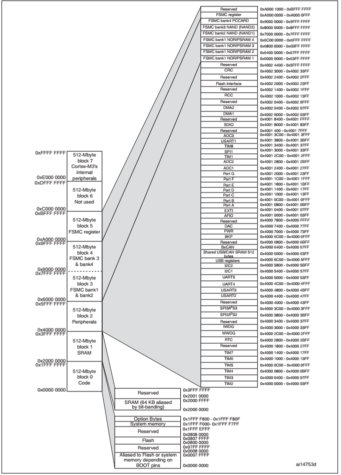
The memory itself does not have address information. Its address is allocated by the chip manufacturer or user. The process of allocating address to the memory is called memory mapping, as shown in the figure below.
Memory map
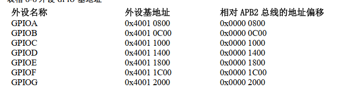
GPIO (general purpose input / output) is the abbreviation of general purpose input / output port. It is located on the APB2 bus peripheral of memory Block2. It is a STM32 controllable pin. Its basic function is to control the pin to output high level or low level.
Chip architecture diagram
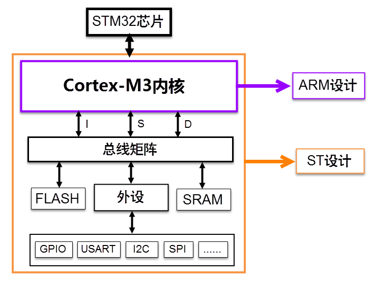
In the memory Block2 area, on-chip peripherals are designed. They take four bytes as a unit, with a total of 32bit. Each unit corresponds to different functions. When we control these units, we can drive the peripherals. We can find the starting address of each unit, and then access these units through the operation mode of C language pointer. If we access these units through this address every time, it is not only bad memory, but also easy to make mistakes. At this time, we can give an alias to this memory unit in the name of function according to the different functions of each unit, This alias is what we often call a register. The process of aliasing memory units with specific functions that have been assigned addresses is called register mapping.
2, GPIO address mapping
1. Bus base address
On chip peripherals are divided into three buses. According to different peripheral speeds, different buses mount different peripherals, APB1 mount low-speed peripherals, APB2 and AHB mount high-speed peripherals. The lowest address of the corresponding bus is called the base address of the bus, which is the address of the first peripheral mounted on the bus.
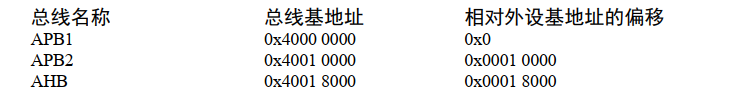
2. Peripheral base address
Various peripherals are mounted on the bus, and these peripherals also have their own address range.
3. Peripheral register
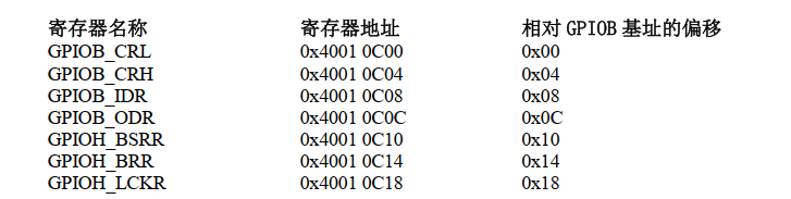
The position of the register is described by the offset address relative to the peripheral base address
State.
During programming, we need to repeatedly refer to the register description of peripheral devices and the register description of specific chapters in STM32F10xx reference manual.
How to calculate the address of a register?
In GPIOA_ Taking bsrr as an example, if the base address of GPIOA peripheral is 0x40010800, we can calculate the GPIOA of GPIOA_ The address of bsrr register is 0x40010800+0x18 (offset from GPIOA base address).
3, C language encapsulation of registers
1. Package bus and peripheral base address
The bus base address and peripheral base address are defined with corresponding macros. The bus or peripheral takes their names as macro names for easy understanding and memory.
 /* Peripheral base address */
#define PERIPH_BASE ((unsigned int)0x40000000)

/* Bus base address */
#define APB1PERIPH_BASE PERIPH_BASE
#define APB2PERIPH_BASE (PERIPH_BASE + 0x00010000)
#define AHBPERIPH_BASE (PERIPH_BASE + 0x00020000)


/* GPIO Peripheral base address */
#define GPIOA_BASE (APB2PERIPH_BASE + 0x0800)
#define GPIOB_BASE (APB2PERIPH_BASE + 0x0C00)
#define GPIOC_ Base (appb2periph_base + 0x1000) zero dead angle
#define GPIOD_BASE (APB2PERIPH_BASE + 0x1400)
#define GPIOE_BASE (APB2PERIPH_BASE + 0x1800)
#define GPIOF_BASE (APB2PERIPH_BASE + 0x1C00)
#define GPIOG_BASE (APB2PERIPH_BASE + 0x2000)


/* Register base address, taking GPIOB as an example */
#define GPIOB_CRL (GPIOB_BASE+0x00)
#define GPIOB_CRH (GPIOB_BASE+0x04)
#define GPIOB_IDR (GPIOB_BASE+0x08)
#define GPIOB_ODR (GPIOB_BASE+0x0C)
#define GPIOB_BSRR (GPIOB_BASE+0x10)
#define GPIOB_BRR (GPIOB_BASE+0x14)
#define GPIOB_LCKR (GPIOB_BASE+0x18
Firstly, the base address of "peripherals on chip" is defined_ Base, followed by periph_ Add the address offset of each bus to the base to obtain the address apb1periph of APB1 and APB2 buses_ BASE APB2PERIPH_BASE, add the offset of peripheral address to get the peripheral address of GPIOA-G, and finally add the address offset of each register to the peripheral address to get the address of a specific register.
Control GPIOB_BSRR pin 0 outputs high level (BR0 of BSRR register is set to 1)
*(unsigned int *)GPIOB_BSRR = 0x01<<0
2. Package register list
typedef unsigned int uint32_t; /*Unsigned 32-bit variable*/
typedef unsigned short int uint16_t; /*Unsigned 16 bit variable*/
/* GPIO Register list */
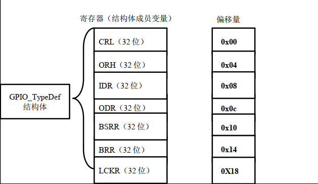
typedef struct {
uint32_t CRL; /*GPIO Port configuration low register address offset: 0x00 */
uint32_t CRH; /*GPIO Port configuration high register address offset: 0x04 */
uint32_t IDR; /*GPIO Address offset of data input register: 0x08 */
uint32_t ODR; /*GPIO Address offset of data output register: 0x0C */
uint32_t BSRR; /*GPIO Bit set / clear register address offset: 0x10 */
uint32_t BRR; /*GPIO Port bit clear register address offset: 0x14 */
uint16_t LCKR; /*GPIO Port configuration lock register address offset: 0x18 */
} GPIO_TypeDef;
The syntax of C language stipulates that the storage space of variables in the structure is continuous, in which 32-bit variables occupy 4 bytes and 16 bit variables occupy 2 bytes. According to the above definition, the offset relative to the base address between member variables is hidden in the variable type.
GPIO_ Address offset map of typedef structure members
Accessing registers through structure pointers
GPIO_TypeDef * GPIOx; //Define a GPIO_TypeDef structure pointer GPIOx
GPIOx = GPIOB_BASE; //Set pointer address to macro GPIOH_BASE address
GPIOx->IDR = 0xFFFF;
GPIOx->ODR = 0xFFFF;
4, Initialization of GPIO port and related principles
1. Clock configuration
There are many peripherals in STM32. In order to reduce power consumption, each peripheral corresponds to a clock. These clocks are turned off when the chip is just powered on. If you want the peripherals to work, you must turn on the corresponding clock. The clocks of all peripherals of STM32 are managed by a special peripheral, called RCC. All gpios are attached to APB2 bus, and the specific clock is controlled by APB2 peripheral clock enable register (RCC_
APB2ENR).
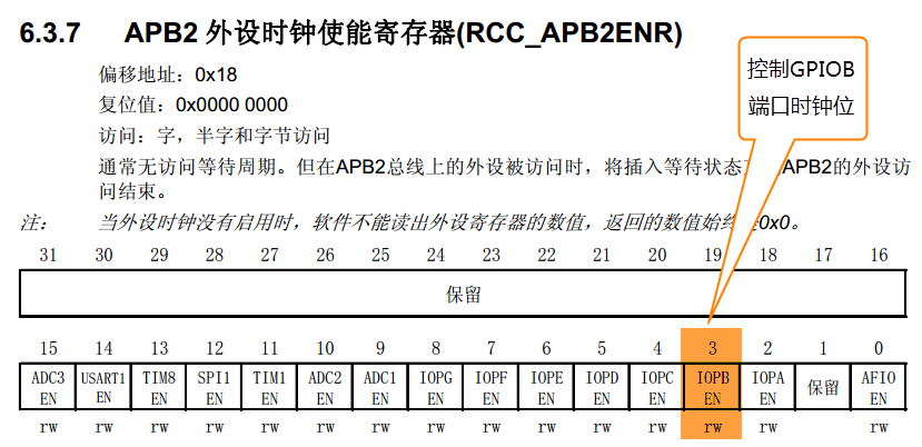
The clock can be turned on by the following code
RCC_APB2ENR |= (1<<3);
2. Input / output mode setting and maximum rate setting
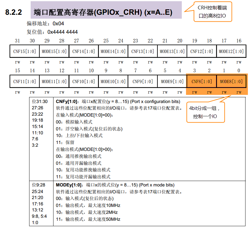
In GPIO peripherals, the high and low control registers CRH and CRL of the control port can configure the working mode and speed of each GPIO. One IO is controlled every four bits, the high eight bits of the CRH control port and the low eight bits of the CRL control port.
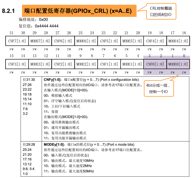
PBn can be configured as universal push-pull output through the following code, and the output speed is 10M (0001)
Using bit operation can avoid affecting other bits in the register, because the register cannot be read and written by bit.
 GPIOB_CRL &= ~( 0x0F<< (4*n));//Clear
 GPIOB_CRL |= (1<<4*n);// PB0 is configured as universal push-pull output with a speed of 10M
3. Control pin output level
Here, GPIO is controlled through the output of ODR register.
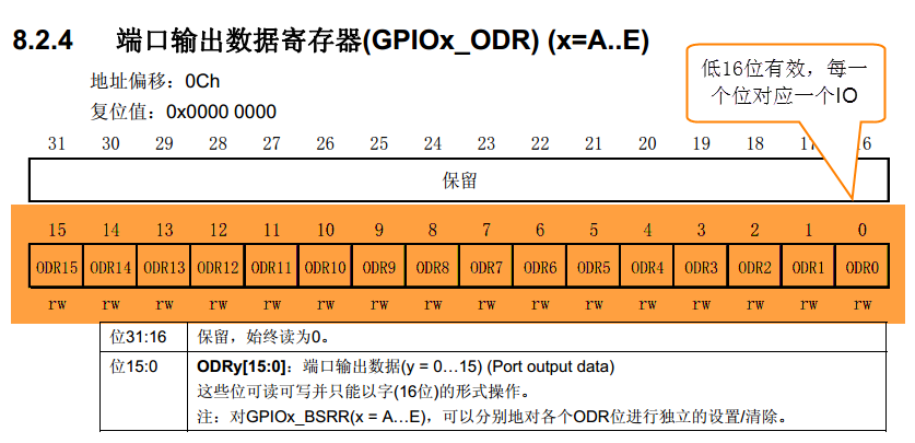
The PBn output low level can be controlled by the following code
GPIOB_ODR &= ~(1<<n);
4, Implementation process
1. Preparation of materials
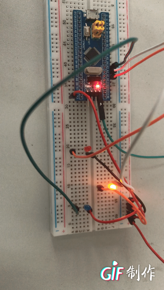
Bread board, LED light, STM32F103C8T6, DuPont cable, USB to serial port
2. Create project
3. Specific code implementation
1)C language programming to realize water lamp
2) Assembly language implementation of water lamp
4. Burning
5. Wiring
6, Experimental effect
7, Summary
After having a systematic understanding of the GPIO port, the register operation of the GPIO port is not difficult, but there is some trouble in finding the address. You need to check the manual. The encapsulation of registers and related library functions in C language can well solve this problem. We should know what it is and why it is. Therefore, we still need to know how to directly operate registers to control GPIO ports, so that we can better use relevant knowledge later. This water lamp is also an introduction to my STM32. The code is written, and the wiring is not very complicated. The next article introduces how to use Keil5's simulation oscilloscope to analyze the code.
8, References
My board is not wild fire, but many materials in the whole process, such as the chip manual, are downloaded from here. The reference book is "zero dead corner playing STM32F103 - Guide", which is written in detail and arranged reasonably.
Wildfire STM32F103C8T6 core board data download