Universal synchronous asynchronous transceiver (USART)
USART introduction
- Full duplex asynchronous communication.
- The interface is connected with other devices through three pins (receive Rx, send TX and clock output CK) (at least RX and TX are required for any USART two-way communication)
- The sender provides a clock for synchronous transmission.
- The transmission and reception are driven by a common baud rate generator. When the enable bits of the transmitter and receiver are set respectively, clocks are generated for them respectively.
Baud rate
- Fractional baud rate generator system
- Programmable baud rate shared by sending and receiving, up to 4.5Mbits/s
- Representation of 12 digit integers and 4-digit decimals.
- Only USART1 uses pclk2 (i.e. APB2 up to 72MHz). Other USARTs use pclk1 (i.e. APB1 up to 36MHz).
- Programmable data word length (8 or 9 bits) (8 data + n stop bit / 9 data + n stop bit) (the last data bit may be parity bit) (the least significant bit of data is first)
- Configurable stop bits - supports 1 or 2 stop bits.
Sending and receiving data flow: (data register USART_DR includes sending register TDR and receiving register RDR)
- Sending data: the system writes the data into the sending register TDR, and then TDR transfers the data to the sending shift register, which is sent to the encoding and decoding module for encoding and output from TX.
- Receiving data; The data is entered from RX, decoded in the encoding and decoding module, and then sent to the receiving shift register, and then to the receiving register RDR for the system to read.
- When the transmit enable bit (TE) is set, the data in the transmit shift register is output on the TX pin and the corresponding clock pulse is output on the CK pin.
- Note: the TE bit cannot be reset during data transmission, otherwise the data on the TX pin will be destroyed because the baud rate counter stops counting. The current data being transferred will be lost.
Calculation of fractional baud rate
- Baud rate = PCK / (16*USARTDIV) (USARTDIV is the value converted from baud ratio register, i.e. frequency division coefficient)
Known USARTDIV = 25.62; Find baud ratio register USART_BRR the value to be written.
- DIV_Fraction = 16*0.62 = 9.92. The nearest integer is: 10 = 0xA
- DIV_ Manssa = 0x25 (rounded) = 0x25. (the integer part is 12 bits, so it's 0x019. It's OK to write 0x19 for easy identification.)
- So USART_BRR = 0x019A (writing 0x19A is also OK)
Interrupt request from USART
- Various interrupt events of USART are connected to the same interrupt vector
Interrupts will be triggered under the following conditions: (if the corresponding enable control bit is set, these events can generate their own interrupts)
- During transmission: the transmission is completed, the transmission is cleared, and the transmission data register is empty.
- During reception: idle bus detection, overflow error, non empty received data register, check error, LIN disconnection symbol detection, noise flag (only in multi buffer communication) and frame error (only in multi buffer communication).
USART register
Status register (USART_SR)
- Reset value: 0xc0
TXE: whether the transmission register DTR is null flag bit.
- When the data in the TDR register is transferred to the shift register by hardware, this bit is set by hardware.
- If the control register USART_ If TXEIE in CR1 is 1, an interrupt is generated.
- For data register USART_ For Dr write operation, the hardware will clear this bit.
- 1: The data has been transferred to the shift register.
TC: send completion flag bit.
- When a frame of data is transmitted and TXE=1, this bit is set to one by the hardware.
- If the control register USART_ If TXEIE in CR1 is 1, an interrupt is generated.
- Clear this bit by the software sequence (read USART_SR first and then write USART_DR)
- 1: Sending completed.
RXNE: check whether the receive shift register is a null flag bit.
- When the data in the receive shift register is transferred to the receive data register RDR, the bit is set by the hardware (empty in the receive shift register)
- If the control register USART_ If RXNEIE in CR1 is 1, an interrupt is generated.
- For data register USART_ The read operation of DR can clear this bit.
- 1: After receiving the data, it can be read out.
IDLE: bus IDLE flag bit detected.
- When bus idle is detected, this bit is set by hardware.
- If USART_ If IDLEIE in CR1 is 1, an interrupt is generated.
- This bit is cleared by the software sequence (read USART_SR first, then USART_DR).
- 1: Idle bus detected.
Data register (USART_DR)
- Reset value: uncertain
- DR: data value, including the data sent or received.
Baud ratio register (USART_BRR)
- Reset value: 0x0000
- DIV_Mantissa: integer part of USARTDIV
- DIV_Fraction: fractional part of USARTDIV
Control register 1(USART_CR1)
- Reset value: 0x0000
- UE: USART enable bit. This bit is set and cleared by software. (0: USART divider and output are disabled)
- M: Set the transmission word length, which is set and cleared by the software (0:8 data bits. 1:9 data bits)
- PCE: inspection control enable (1: enable verification control)
- PS: check selection (0: even check)
- PEIE: PE interrupt enable (1: when TXE in USART_SR is 1, USART interrupt is generated)
- TCIE: send completion interrupt enable (1: USART interrupt is generated when TC in USART_SR is 1)
- RXNEIE: receive interrupt enable with empty shift register (1: generate USART interrupt when ORE or RXNE in USART_SR is 1)
- IDLEIE: bus IDLE idle interrupt enable (this bit is set or cleared by software) (1: when IDLE in USART_SR is 1, USART interrupt is generated)
- TE: send enable (1: enable send)
- RE: receive enable (1: enable receive and start searching for the start bit on RX pin)
Control register 2(USART_CR2)
- Reset value: 0x0000
STOP: STOP bit (UART4 and UART5 cannot use 0.5 STOP bit and 1.5 STOP bit)
- 00:1 stop bit.
- 01: 0.5 stop bits.
- 10: 2 stop bits.
- 11: 1.5 stop bits
- CLKEN: clock enable (0: disable CK pin)
Code example
- USART initialization settings
/*******************************************************************************
* Function name: USART1_Init
* Function: USART1 initialization function
* Input: bound: baud rate
* Output: None
*******************************************************************************/
void USART1_Init(u32 bound)
{
   //GPIO port settings
    GPIO_InitTypeDef GPIO_InitStructure;    //Declare GPIO objects
    USART_InitTypeDef USART_InitStructure;    //Declare serial port object
    NVIC_InitTypeDef NVIC_InitStructure;    //Declare nested broken objects

    RCC_APB2PeriphClockCmd(RCC_APB2Periph_GPIOA,ENABLE);
    RCC_APB2PeriphClockCmd(RCC_APB2Periph_USART1,ENABLE);


    /*  Configure GPIO mode and IO port */
    GPIO_InitStructure.GPIO_Pin=GPIO_Pin_9;//TX / / serial port output PA9
    GPIO_InitStructure.GPIO_Speed=GPIO_Speed_50MHz;
    GPIO_InitStructure.GPIO_Mode=GPIO_Mode_AF_PP;        //Multiplex push-pull output
    GPIO_Init(GPIOA,&GPIO_InitStructure);  /* Initialize serial port output PA9*/

    GPIO_InitStructure.GPIO_Pin=GPIO_Pin_10;//RX / / serial port input PA10
    GPIO_InitStructure.GPIO_Mode=GPIO_Mode_IN_FLOATING;          //Analog input
    GPIO_Init(GPIOA,&GPIO_InitStructure); /* Initialize serial port input PA10*/


   //USART1 initialization settings
    USART_InitStructure.USART_BaudRate = bound;//Baud rate setting
    USART_InitStructure.USART_WordLength = USART_WordLength_8b;//The word length is in 8-bit data format
    USART_InitStructure.USART_StopBits = USART_StopBits_1;//A stop bit
    USART_InitStructure.USART_Parity = USART_Parity_No;//No parity bit
    USART_InitStructure.USART_HardwareFlowControl = USART_HardwareFlowControl_None;//No hardware data flow control
    USART_InitStructure.USART_Mode = USART_Mode_Rx | USART_Mode_Tx;    //Transceiver mode
    USART_Init(USART1, &USART_InitStructure); //Initialize serial port 1

    USART_Cmd(USART1, ENABLE);  //Enable serial port 1

    USART_ClearFlag(USART1, USART_FLAG_TC);  //Clear the pending flag of the serial port

    USART_ITConfig(USART1, USART_IT_RXNE, ENABLE);//Turn on related interrupt

    //Usart1 NVIC configuration
    NVIC_InitStructure.NVIC_IRQChannel = USART1_IRQn;        //Serial port 1 interrupt channel
    NVIC_InitStructure.NVIC_IRQChannelPreemptionPriority=3; //Preemption priority 3
    NVIC_InitStructure.NVIC_IRQChannelSubPriority =3;        //Sub priority 3
    NVIC_InitStructure.NVIC_IRQChannelCmd = ENABLE;            //IRQ channel enable
    NVIC_Init(&NVIC_InitStructure);    //Initializes the VIC register according to the specified parameters
}
- Interrupt function of serial port
/*******************************************************************************
* Function name: USART1_IRQHandler
* Function: USART1 interrupt function
* Input: None
* Output: None
*******************************************************************************/
void USART1_IRQHandler(void)                    //Serial port 1 interrupt service program
{
    u8 r;
    if(USART_GetITStatus(USART1, USART_IT_RXNE) != RESET)  //Receive interrupt
    {
        r =USART_ReceiveData(USART1);//(USART1->DR);    // Read received data
        USART_SendData(USART1,r);          //    Send the received data back
        while(USART_GetFlagStatus(USART1,USART_FLAG_TC) != SET);
    }
    USART_ClearFlag(USART1,USART_FLAG_TC);
}
EEPROM for I2C communication
I2C features
- It follows the same I2C protocol as 51 single chip microcomputer.
- The interface is connected to I2C bus through data pin (SDA) and clock pin (SCL) (data pin SDA is used for data transmission, and clock pin SCL is used for synchronization of sending and receiving data)
- The I2C module receives and sends data and converts the data from serial to parallel or parallel to serial.
I2C main equipment functions:
- Generate clock.
- Generate start and stop signals.
I2C slave functions:
- Programmable I2C address detection.
- Dual address capability to respond to 2 slave addresses.
- Stop bit detection.
Support different communication speeds:
- Standard speed (up to 100 kHz)
- Fast (up to 400 kHz)
Status flag:
- Transmitter / receiver mode flag.
- Byte send end flag.
- I2C bus busy flag.
Error flag:
- Arbitration lost in main mode.
- Reply (ACK) error after address / data transmission.
- Start or stop condition of dislocation detected.
- It is forbidden to overflow or underflow when lengthening the clock function.
Has 2 interrupt vectors:
- 1 interrupt for address / data communication success.
- Used for 1 interrupt.
I2C communication process
1. The host sends the I2C start signal (through SDA line) and generates a clock signal to tell the slave to start transmitting the signal (all slaves will receive this start signal)
2. At this time, the master will broadcast the slave address (each slave address is unique) (one or two bytes after the starting condition is the address), and the corresponding slave address will give a response signal after matching.
3. When sending the slave address, the device will also tell the slave whether to send data or receive data (TRA bit indicates whether the master device is in receiver mode or transmitter mode)
4. In 7-bit address mode:- Enter the send data mode: when the master device sends the slave address, the lowest bit is' 0 '.
- Enter the data receiving mode: the lowest bit is' 1 'when the master device sends the slave address.
5. In 10 bit address mode:
- Enter the data sending mode: the master device sends the header byte (11110xx0) first, and then the slave address with the lowest bit of '0' (where XX represents the highest 2 bits of the 10 bit address)
- Enter the data receiving mode: the master device sends the header byte (11110xx0) first, and then the slave address with the lowest bit of '1'. Then resend a start condition, followed by the header byte (11110xx1) (where XX represents the highest 2 bits of the 10 bit address)
6. Slave device address agreement:
- The upper 4 bits of the 8-bit slave device address are fixed to 1010, the next 3 bits represent the address of the memory to be read and written, and the last bit is the read-write control bit (1 represents read)
7. If the slave agrees, it can communicate.
8. When the communication is stopped, the host will send a stop signal to tell the slave that it is over.
I2C mode selection
Four operation modes: (the module works in slave mode by default)
- Slave transmitter mode
- Slave receiver mode
- Main transmitter mode
- Master receiver mode
- Note: the interface automatically switches from the slave mode to the main mode after generating the starting condition; When the arbitration is lost or a stop signal is generated, it is switched from the master mode to the slave mode.
- Data transmission process: serial data transmission always starts with the START condition and ends with the stop condition, and the receiver must respond to an ACK to the transmitter on the ninth clock after 8 clocks of one byte transmission. When the START condition is generated on the bus through the START bit, the device enters the main mode. (device default slave mode)
I2C interrupt request
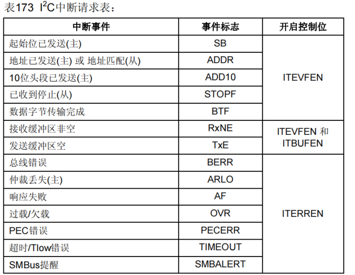
- SB, ADDR, ADD10, STOPF, BTF, RxNE and TxE use the same interrupt channel through logic or (it_event interrupt)
- BERR, ARLO, AF, OVR, PECERR, TIMEOUT and SMBALERT use the same interrupt channel through logic or (it_error interrupt)
I2C register description
Control register 1 (I2C_CR1)
- Reset value: 0x0000
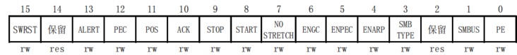
SWRST: software reset
- When set, I2C is in the reset state. Before resetting this bit, make sure that the I2C pin is released and the bus is empty
- 0: I2C module is not in reset state
- 1: I2C module is in reset state
ACK: reply enable
- This bit can be set or cleared by software, or cleared by hardware when PE=0
- 0: no reply returned
- 1: Returns a reply (matching address or data) after receiving a byte
STOP: STOP condition generation
- The software can set or clear this bit
- When a stop condition is detected, it is cleared by the hardware
- When a timeout error is detected, the hardware sets it
- In main mode: 1: generate stop condition after current byte transmission or current start condition is issued
- In slave mode: 1: the stop condition is generated after the current byte is transmitted or the SCL and SDA lines are released
- Note: when the STOP, START or PEC bit is set, the software shall not perform any I2C verification before the hardware clears this bit_ Write operation of CR1; Otherwise, the STOP, START or PEC bits may be set for the second time
START: START condition generation
- The software can set or clear this bit
- When the start condition is issued or PE=0, it is cleared by the hardware
- In the main mode: 1: repeat the start condition
- In slave mode: 1: when the bus is idle, the start condition is generated
- ENGC: broadcast call enable (1: allow broadcast call. Reply to address 00h)
- ENPEC: PEC enable (ENPEC: PEC enable)
ENARP: ARP enable
- 1: Enable ARP
- If SMBTYPE=0, the default address of the SMBus device is used
- If SMBTYPE=1, the primary address of SMBus is used
- SMBTYPE: SMBus type (0: SMBus device; 1: SMBus host)
- SMBUS: SMBUS mode (0: I2C mode; 1: SMBUS mode)
- PE: I2C module enable (1: enable I2C module. According to the setting of SMBUS bit, the corresponding I/O port needs to be configured as multiplexing function)
Control register 2(I2C_CR2)
- Reset value: 0x0000
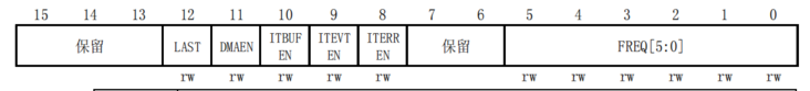
- Last: last DMA transfer (1: EOT of the next DMA is the last transfer)
- DMAEN: DMA request enable (1: DMA request is allowed when TxE=1 or RxNE =1)
- ITBUFEN: buffer interrupt enable (1: event interrupt is generated when TxE=1 or RxNE=1, regardless of DMAEN status)
- ITEVTEN: event interrupt enable (1: allow event interrupt)
- ITERREN: error interrupt enable (1: allow error interrupt)
FREQ[5:0]: clock frequency of I2C module (correct input clock frequency must be set to generate correct timing, ranging from 2 to 36MHz)
- 000000: Disabled
- 00000 1: Disabled
- 000010: 2MHz
- .......
- 100100: 36MHz
- Greater than 100 disabled
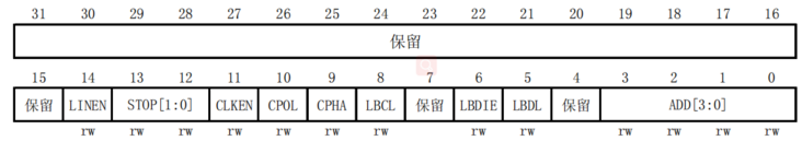
Self address register 1(I2C_OAR1)
- Reset value: 0x0000
ADDMODE: addressing mode (in slave mode)
- 0: 7-bit slave address (no response to 10 bit address)
- 1: 10 bit slave address (no response to 7-bit address)
- Bit 14: must always be held to 1 by the software.
ADD[9:8]: interface address
- Don't care in 7-bit address mode
- 9-8 bits of address in 10 bit address mode
- ADD[7:1]: interface address (7 ~ 1 bits of address)
ADD0: interface address
- Don't care in 7-bit address mode
- Bit 0 of address in 10 bit address mode
Data register (I2C_DR)
- Reset value: 0x0000

DR: 8-bit data register
- It is used to store the received data or place the data sent to the bus
Status register 1(I2C_SR1)
- Reset value: 0x0000
- SMBALERT: SMBus reminder
- TIMEOUT: TIMEOUT or Tlow error
- PECERR: PEC error occurred while receiving
- OVR: overload / underload
- AF: reply failed
- ARLO: Arbitration lost (main mode)
- BERR: bus error
- TxE: data register is empty (when sending)
- RxNE: data register is not empty (when receiving)
- STOPF: stop condition detection bit (slave mode)
- ADD10: 10 bit header sequence sent (main mode)
- BTF: end of byte sending
- ADDR: address sent (master mode) / address matching (slave mode)
- Start condition: SB
Status register 2 (I2C_SR2)
- Reset value: 0x0000
- PEC[7:0]: packet error detection
- DUALF: Dual Flag (slave mode)
- SMBHOST: SMBus host header series (slave mode)
- SMBDEFAULT: default address of SMBus device (slave mode)
- GENCALL: broadcast call address (slave mode)
- TRA: whether data is sent / received
- BUSY: bus BUSY
- MSL: master-slave mode
Clock control register (I2C_CCR)
- Reset value: 0x0000
be careful:
- FPCLK1 is required to be an integral multiple of 10 MHz, which can correctly generate a fast clock of 400KHz
- CCR register can be set only when I2C is turned off (PE=0)
- F/S: I2C main mode option
- DUTY: DUTY cycle in fast mode
- CCR: clock control frequency division coefficient in fast / standard mode (main mode)
Code example
- I2C code
#include "iic.h"
#include "SysTick.h"

//IO operation function
#define IIC_SCL    PBout(10) //SCL
#define IIC_SDA    PBout(11) //SDA
#define READ_ SDA pbin (11) / / enter SDA


/*******************************************************************************
* Function name: IIC_Init
* Function: IIC initialization
* Input: None
* Output: None
*******************************************************************************/
void IIC_Init(void)
{
    GPIO_InitTypeDef  GPIO_InitStructure;
    RCC_APB2PeriphClockCmd(IIC_SCL_PORT_RCC|IIC_SDA_PORT_RCC,ENABLE);

    GPIO_InitStructure.GPIO_Pin=GPIO_Pin_10;         //Specify PB10 as the SCL line
    GPIO_InitStructure.GPIO_Speed=GPIO_Speed_50MHz;
    GPIO_InitStructure.GPIO_Mode=GPIO_Mode_Out_PP;
    GPIO_Init(GPIOB,&GPIO_InitStructure);                //Initialize I/O port

    GPIO_InitStructure.GPIO_Pin=GPIO_Pin_11;            //Specify PB11 as SDA line
    GPIO_Init(GPIOB,&GPIO_InitStructure);

    IIC_SCL=1;
    IIC_SDA=1;
}

/*******************************************************************************
* Function name: SDA_OUT
* Function function: SDA output configuration
* Input: None
* Output: None
*******************************************************************************/
void SDA_OUT(void)
{
    GPIO_InitTypeDef  GPIO_InitStructure;

    GPIO_InitStructure.GPIO_Pin=GPIO_Pin_11;
    GPIO_InitStructure.GPIO_Speed=GPIO_Speed_50MHz;
    GPIO_InitStructure.GPIO_Mode=GPIO_Mode_Out_PP;
    GPIO_Init(GPIOB,&GPIO_InitStructure);
}

/*******************************************************************************
* Function name: SDA_IN
* Function function: SDA input configuration
* Input: None
* Output: None
*******************************************************************************/
void SDA_IN(void)
{
    GPIO_InitTypeDef  GPIO_InitStructure;

    GPIO_InitStructure.GPIO_Pin=GPIO_Pin_11;
    GPIO_InitStructure.GPIO_Mode=GPIO_Mode_IPU;
    GPIO_Init(GPIOB,&GPIO_InitStructure);
}

/*******************************************************************************
* Function name: IIC_Start
* Function: generate IIC start signal
* Input: None
* Output: None
*******************************************************************************/
void IIC_Start(void)
{
    SDA_OUT();     //SDA line output
    IIC_SDA=1;     //SDA line is pulled high
    IIC_SCL=1;        //SCL line elevation
    delay_us(5);
     IIC_SDA=0;    //When the CLK value is high, SDA changes from high to low, indicating the start signal
    delay_us(6);
    IIC_SCL=0;    //Clamp the I2C bus and prepare to send or receive data
}

/*******************************************************************************
* Function name: IIC_Stop
* Function: generate IIC stop signal
* Input: None
* Output: None
*******************************************************************************/
void IIC_Stop(void)
{
    SDA_OUT();    //sda line output
    IIC_SCL=0;
    IIC_SDA=0;
     IIC_SCL=1;
    delay_us(6);
    IIC_SDA=1;    //When the CLK value is high, SDDA changes from low to high, indicating a stop signal
    delay_us(6);
}

/*******************************************************************************
* Function name: IIC_Wait_Ack
* Function: wait for the arrival of the response signal
* Input: None
* Output: 1. Failed to receive response
                     0,Received reply successfully
*******************************************************************************/
u8 IIC_Wait_Ack(void)
{
    u8 tempTime=0;

    IIC_SDA=1;
    delay_us(1);
    SDA_IN();      //SDA set as input
    IIC_SCL=1;
    delay_us(1);
    while(READ_SDA)
    {
        tempTime++;
        if(tempTime>250)
        {
            IIC_Stop();
            return 1;
        }
    }
    IIC_SCL=0;//Clock output 0
    return 0;
}

/*******************************************************************************
* Function name: IIC_Ack
* Function: generate ACK response
* Input: None
* Output: None
*******************************************************************************/
void IIC_Ack(void)
{
    IIC_SCL=0;
    SDA_OUT();
    IIC_SDA=0;
    delay_us(2);
    IIC_SCL=1;
    delay_us(5);
    IIC_SCL=0;
}

/*******************************************************************************
* Function name: IIC_NAck
* Function function: generate NACK non response
* Input: None
* Output: None
*******************************************************************************/
void IIC_NAck(void)
{
    IIC_SCL=0;
    SDA_OUT();
    IIC_SDA=1;
    delay_us(2);
    IIC_SCL=1;
    delay_us(5);
    IIC_SCL=0;
}

/*******************************************************************************
* Function name: IIC_Send_Byte
* Function function: IIC sends a byte
* Input: txd: Send a byte
* Output: None
*******************************************************************************/
void IIC_Send_Byte(u8 txd)
{
    u8 t;
    SDA_OUT();
    IIC_SCL=0;//Pull down the clock to start data transmission
    for(t=0;t<8;t++)
    {
        if((txd&0x80)>0) //0x80  1000 0000
            IIC_SDA=1;
        else
            IIC_SDA=0;
        txd<<=1;
        delay_us(2);   //These three delays are necessary for TEA5767
        IIC_SCL=1;
        delay_us(2);
        IIC_SCL=0;
        delay_us(2);
    }
}

/*******************************************************************************
* Function name: IIC_Read_Byte
* Function: IIC reads a byte
* Input: when ack=1, send ACK, ack=0, send nACK
* Output: reply or non reply
*******************************************************************************/
u8 IIC_Read_Byte(u8 ack)
{
    u8 i,receive=0;
    SDA_IN();//SDA set as input
    for(i=0;i<8;i++ )
    {
        IIC_SCL=0;
        delay_us(2);
        IIC_SCL=1;
        receive<<=1;
        if(READ_SDA)receive++;
        delay_us(1);
    }
    if (!ack)
        IIC_NAck();//Send nACK
    else
        IIC_Ack(); //Send ACK
    return receive;
}
- AT24C code
#include "24cxx.h"
#include "SysTick.h"

/*******************************************************************************
* Function name: AT24CXX_Init
* Cx24atx function initialization
* Input: None
* Output: None
*******************************************************************************/
void AT24CXX_Init(void)
{
    IIC_Init();//IIC initialization
}

/*******************************************************************************
* Function name: AT24CXX_ReadOneByte
* Function function: read a data at the specified address of AT24CXX
* Input: ReadAddr: address to start reading
* Output: read data
*******************************************************************************/
u8 AT24CXX_ReadOneByte(u16 ReadAddr)
{
    u8 temp=0;
    IIC_Start();
    if(EE_TYPE>AT24C16)
    {
        IIC_Send_Byte(0XA0);       //Send write command (the lowest bit is 0, write to the slave device)
        IIC_Wait_Ack();
        IIC_Send_Byte(ReadAddr>>8);//Send high address
    }
    else
    {
        IIC_Send_Byte(0XA0+((ReadAddr/256)<<1));   //Send device address 0XA0, write data
    }
    IIC_Wait_Ack();
  IIC_Send_Byte(ReadAddr%256);   //Send low address
    IIC_Wait_Ack();
    IIC_Start();                              //Repeat the starting condition and enter the transmission mode from the device
    IIC_Send_Byte(0XA1);                 //Send the device address and the last bit is 1, read from the slave device
    IIC_Wait_Ack();
  temp=IIC_Read_Byte(0);
  IIC_Stop();//Generate a stop condition
    return temp;
}

/*******************************************************************************
* Function name: AT24CXX_WriteOneByte
* Function function: write a data at the specified address of AT24CXX
* Input: WriteAddr: destination address for writing data
                     DataToWrite:Data to write
* Output: None
*******************************************************************************/
void AT24CXX_WriteOneByte(u16 WriteAddr,u8 DataToWrite)
{
    IIC_Start();
    if(EE_TYPE>AT24C16)
    {
        IIC_Send_Byte(0XA0);        //Send write command
        IIC_Wait_Ack();
        IIC_Send_Byte(WriteAddr>>8);//Send high address
    }
    else
    {
        IIC_Send_Byte(0XA0+((WriteAddr/256)<<1));   //Send device address 0XA0, write data
    }
    IIC_Wait_Ack();
  IIC_Send_Byte(WriteAddr%256);   //Send low address
    IIC_Wait_Ack();
    IIC_Send_Byte(DataToWrite);     //Send byte
    IIC_Wait_Ack();
  IIC_Stop();//Generate a stop condition
    delay_ms(10);
}

/*******************************************************************************
* Function name: AT24CXX_WriteLenByte
* Function function: start writing Len data at the specified address in AT24CXX
                     Used to write 16bit or 32bit data
* Input: WriteAddr: destination address for writing data
                     DataToWrite:Data to write
                     Len        :Length of data to be written 2,4
* Output: None
*******************************************************************************/
void AT24CXX_WriteLenByte(u16 WriteAddr,u32 DataToWrite,u8 Len)
{
    u8 t;
    for(t=0;t<Len;t++)
    {
        AT24CXX_WriteOneByte(WriteAddr+t,(DataToWrite>>(8*t))&0xff);
    }
}

/*******************************************************************************
* Function name: AT24CXX_ReadLenByte
* Function function: start reading data with length Len at the specified address in AT24CXX
                     It is used to read out 16bit or 32bit data
* Input: ReadAddr: address to start reading
                     Len        :Length of data to be read 2,4
* Output: read data
*******************************************************************************/
u32 AT24CXX_ReadLenByte(u16 ReadAddr,u8 Len)
{
    u8 t;
    u32 temp=0;
    for(t=0;t<Len;t++)
    {
        temp<<=8;
        temp+=AT24CXX_ReadOneByte(ReadAddr+Len-t-1);
    }
    return temp;
}

/*******************************************************************************
* Function name: AT24CXX_Check
* Function: check whether AT24CXX is normal
* Input: None
* Output: 1: detection failed, 0: detection succeeded
*******************************************************************************/
u8 AT24CXX_Check(void)
{
    u8 temp;
    temp=AT24CXX_ReadOneByte(255);//Avoid writing AT24CXX every time you power on
    if(temp==0x36)return 0;
    else//Exclude the first initialization
    {
        AT24CXX_WriteOneByte(255,0X36);
        temp=AT24CXX_ReadOneByte(255);
        if(temp==0X36)return 0;
    }
    return 1;
}

/*******************************************************************************
* Function name: AT24CXX_Read
* Function function: start reading the specified number of data at the specified address in AT24CXX
* Input: ReadAddr: the address pair 24c02 to be read is 0 ~ 255
                     pBuffer  :First address of data array
                     NumToRead:Number of data to be read out
* Output: None
*******************************************************************************/
void AT24CXX_Read(u16 ReadAddr,u8 *pBuffer,u16 NumToRead)
{
    while(NumToRead)
    {
        *pBuffer++=AT24CXX_ReadOneByte(ReadAddr++);
        NumToRead--;
    }
}

/*******************************************************************************
* Function name: AT24CXX_Write
* Function function: start writing a specified number of data at the specified address in AT24CXX
* Input: WriteAddr: the address to start writing is 0 ~ 255 for 24c02
                     pBuffer  :First address of data array
                     NumToRead:Number of data to be read out
* Output: None
*******************************************************************************/
void AT24CXX_Write(u16 WriteAddr,u8 *pBuffer,u16 NumToWrite)
{
    while(NumToWrite--)
    {
        AT24CXX_WriteOneByte(WriteAddr,*pBuffer);
        WriteAddr++;
        pBuffer++;
    }
}