Previously, we verified that the program runs in SRAM, that is, the program runs in L2 cache, but for starting the operating system, this is not enough. The operating system must have enough ram, so we must run the program in RAM, that is DDR.
Environmental Science
-
CodeWarriorDevelopmentStudio for Power Architecture v10.5.1 - Windows.exe
-
CodeWarrior Connection Server
-
Ethernet Tap
- CodeWarrior is installed and the license is not expired
- Ethernet Tap is connected correctly
- CodeWarrior Connection Server is connected correctly
Verification
-
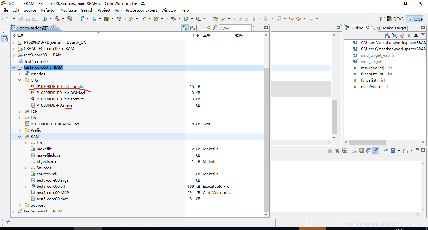
RAM verification is that the program runs in DDR. As above, create a project of downloading RAM, or modify the debug configuration to add a RAM configuration.
-
First, try debug ging to run the following. If the pcb board is moved according to the official board, it can be run directly. If not, you need to modify tcl files and mem files
-
The ddr parameter of tcl needs to use QCVS to verify the generation
Attached my revised tcl
     ########################################################################################
     # Initialization file for P1020RDB-PD board
     # Clock Configuration:
     #       CPU0: 800 MHz, CPU1:800 MHz, CCB: 400 MHz,
     #       DDR: 667/800 MHz, SYSCLK: 66 MHz
     ########################################################################################

     variable CCSRBAR 0xff700000

     proc CCSR {reg_off} {
     	global CCSRBAR

     	return p:0x[format %x [expr {$CCSRBAR + $reg_off}]]
     }

     proc apply_e500v2_workaround {} {
     	# After reset, e500 cores need to run before being able to enter debug mode.
     	# Work-around: set a HW BP at reset address and run the core; after the core hits the BP, it enters debug mode
     	# e500 cores need to have valid opcode at the interrupt vector

     	variable SPR_GROUP "e500 Special Purpose Registers/"

     	#######################################################################
     	# Set a breakpoint at the reset address
     	reg ${SPR_GROUP}IAC1 = 0xfffffffc
     	reg ${SPR_GROUP}DBCR0 = 0x40800000
     	reg ${SPR_GROUP}DBCR1 = 0x00000000

     	# Run the core
     	config runcontrolsync off
     	go
     	wait 50
     	config runcontrolsync on
     	stop

     	# Clear affected registers
     	reg ${SPR_GROUP}DBSR  = 0x01CF0000
     	reg ${SPR_GROUP}DBCR0 = 0x41000000
     	reg ${SPR_GROUP}IAC1  = 0x00000000
     	reg ${SPR_GROUP}CSRR0 = 0x00000000
     	reg ${SPR_GROUP}CSRR1 = 0x00000000
     }

     proc init_board {} {

     	global CCSRBAR

     	# bits 4-7 - ROM_LOC
     	# 1000 Local bus FCM 8-bit NAND flash small page
     	# 1010 Local bus FCM 8-bit NAND flash large page
     	# 1101 Local bus GPCM 8-bit ROM
     	# 1110 Local bus GPCM 16-bit ROM
     	# 1111 Local bus GPCM 16-bit ROM (default)
     	# using PORBMSR registers from Global Utilities
     	variable ROM_LOC					0x[format %x [expr {[mem [CCSR 0xe0004] -np] & 0x0f000000}]]
     	variable FCM_SMALL_PAGE_BOOT_LOC 	"0x08000000"
     	variable FCM_LARGE_PAGE_BOOT_LOC 	"0x0A000000"
     	variable GPCM_8BIT_BOOT_LOC	 		"0x0D000000"
     	variable GPCM_16BIT_BOOT_LOC	 	"0x0E000000"

     	variable BOOT_DEVICE		0x[format %x [expr {$ROM_LOC & 0x0c000000 }]]
     	variable NAND_BOOT_DEVICE 	"0x08000000"
     	variable NOR_BOOT_DEVICE 	"0x0c000000"

     	# configure local access windows

     	# LAWBAR0 - Local Bus (NOR)
     	# bit 8 - 31 = 0xF8000000 - base addr,the 24 high-order address of 36bits phaysical %%%
     	mem [CCSR 0xc08] = 0x000f8000

     	# LAWAR0
     	# bit 0 = 1 - enable window
     	# bit 7-11 = 00100 - Local Bus NOR
     	# bit 26 - 31 =  011001 64M - size
     	mem [CCSR 0xc10] = 0x8040001A

     	# LAWBAR1 - PEX1
     	# bit 8 - 31 = 0x80000000 - base addr
     	mem [CCSR 0xc28] = 0x000a0000

     	# LAWAR1
     	# bit 0 = 1 - enable window
     	# bit 7-11 = 00010 - PEX1
     	# bit 26 - 31 =  011100 512M - size
     	mem [CCSR 0xc30] = 0x8020001c

     	# LAWBAR2 - PEX 1
     	# bit 8 - 31 = 0xEFC00000 - base addr
     	mem [CCSR 0xc48] = 0x000efc00

     	# LAWAR2
     	# bit 0 = 1 - enable window
     	# bit 7-11 = 00010 - PEX 1
     	# bit 26-31 = 001111 64k - size
     	mem [CCSR 0xc50] = 0x80200010


     	# LAWBAR3 - PEX2
     	# bit 8 - 31 = 0xA0000000 - base addr
     	mem [CCSR 0xc68] = 0x00080000

     	# LAWAR3
     	# bit 0 = 1 - enable window
     	# bit 7-11 = 00001 - PEX2
     	# bit 26 - 31 =  011100 512M - size
     	mem [CCSR 0xc70] = 0x8010001c

     	# LAWBAR4 - PEX 2
     	# bit 8 - 31 = 0xEFC10000 - base addr
     	mem [CCSR 0xc88] = 0x000efc20

     	# LAWAR4
     	# bit 0 = 1 - enable window
     	# bit 7-11 = 00001 - PEX 2
     	# bit 26-31 = 001111 64k - size
     	mem [CCSR 0xc90] = 0x80100010

     	# LAWBAR5 - CPLD
     	# bit 8 - 31 = 0xEFA00000 - base addr
     	mem [CCSR 0xca8] = 0x000efd00

     	# LAWAR5
     	# bit 0 = 1 - enable window
     	# bit 7-11 = 00100 - Local Bus CPLD
     	# bit 26-31 = 010011 1M - size
     	mem [CCSR 0xcb0] = 0x8040000f

     	# LAWBAR6 - Local Bus NAND
     	# bit 8 - 31 = 0xEFF00000 - base addr
     	mem [CCSR 0xcc8] = 0x000efa00

     	# LAWAR6
     	# bit 0 = 1 - enable window
     	# bit 7-11 = 00100 - IFC - Local Bus NAND
     	# bit 26-31 = 010011 1M - size
     	mem [CCSR 0xcd0] = 0x80400011

     	# LAWBAR7 - Local Bus  FPGA_reg
     	# bit 8 - 31 = 0xEFB00000 - base addr
     	mem [CCSR 0xce8] = 0x000efb00

     	# LAWAR7
     	# bit 0 = 1 - enable window
     	# bit 7-11 = 00100 - eLBC - Local Bus FPGA_reg
     	# bit 26-31 = 010001 256k - size
     	mem [CCSR 0xcf0] = 0x80400011

     	# LAWBAR8 - DDR3
     	# bit 8 - 31 = 0x00000000 - base addr
     	mem [CCSR 0xd08] = 0x00000000

     	# LAWAR8
     	# bit 0 = 1 - enable window
     	# bit 7-11 = 01111 - DDR3
     	# bit 26 - 31 =  011101 1G - size
     	mem [CCSR 0xd10] = 0x80F0001d

     	##################################################################################
     	# DDR Controllers Setup

     	# using PORPLLSR registers from Global Utilities to choose between different DDR Controllers Setups Freqs
     	variable DDR_ratio_800 0x1800
     	variable DDR_ratio_677 0x1400

     	variable DDR_ratio 0x[format %x [expr {[mem [CCSR 0xe0000] -np] & 0x00003E00}]]

     	if { $DDR_ratio == $DDR_ratio_677 } {

     		# DDR_SDRAM_CFG
     		mem [CCSR 0x2110] = 0x470c0008

     		#CS0_BNDS
     		mem [CCSR 0x2000] = 0x0000003f

     		#CS1_BNDS
     		mem [CCSR 0x2008] = 0x00000000

     		#CS0_CNFG
     		mem [CCSR 0x2080] = 0x80014302

     		#CS1_CNFG
     		mem [CCSR 0x2084] = 0x00000000

     		# TIMING_CFG_0
     		mem [CCSR 0x2104] = 0x00330104

     		# TIMING_CFG_1
     		mem [CCSR 0x2108] = 0x9891BA45

     		# TIMING_CFG_2
     		mem [CCSR 0x210c] = 0x0fB8A914

     		# TIMING_CFG_3
     		mem [CCSR 0x2100] = 0x01051000

     		# TIMING_CFG_4
     		mem [CCSR 0x2160] = 0x00000001

     		# TIMING_CFG_5
     		mem [CCSR 0x2164] = 0x00005400

     		# DDR_SDRAM_CFG_2
     		mem [CCSR 0x2114] = 0x24401010

     		# DDR_SDRAM_MODE
     		mem [CCSR 0x2118] = 0x40441A50

     		# DDR_SDRAM_MODE_2
     		mem [CCSR 0x211c] = 0x8010C000

     		# DDR_SDRAM_MD_CNTL
     		mem [CCSR 0x2120] = 0x00000000

     		# DDR_SDRAM_INTERVAL
     		mem [CCSR 0x2124] = 0x0a280100

     		# DDR_DATA_INIT
     		mem [CCSR 0x2128] = 0xA9AB1005

     		# DDR_SDRAM_CLK_CNTL
     		mem [CCSR 0x2130] = 0x01000000

     		# DDR_ZQ_CNTL
     		mem [CCSR 0x2170] = 0x89080600

     		# DDR_WRLVL_CNTL
     		mem [CCSR 0x2174] = 0x8645C605

     		# DDR_CDR_1
     		mem [CCSR 0x2b28] = 0x00000000

     		# DDR_CDR_2
     		mem [CCSR 0x2b2c] = 0x00000000
     	}

     	if { $DDR_ratio == $DDR_ratio_800 } {

     		# DDR_SDRAM_CFG
     		mem [CCSR 0x2110] = 0x470c0008

     		#CS0_BNDS
     		mem [CCSR 0x2000] = 0x0000003f

     		#CS1_BNDS
     		mem [CCSR 0x2008] = 0x00000000

     		#CS0_CNFG
     		mem [CCSR 0x2080] = 0x80014302

     		#CS1_CNFG
     		mem [CCSR 0x2084] = 0x00000000

     		# TIMING_CFG_0
     		mem [CCSR 0x2104] = 0x00110104

     		# TIMING_CFG_1
     		mem [CCSR 0x2108] = 0x6f6b8644

     		# TIMING_CFG_2
     		mem [CCSR 0x210c] = 0x0fa888cf

     		# TIMING_CFG_3
     		mem [CCSR 0x2100] = 0x00030000

     		# DDR_SDRAM_CFG_2
     		mem [CCSR 0x2114] = 0x24401010

     		# DDR_SDRAM_MODE
     		mem [CCSR 0x2118] = 0x00441420

     		# DDR_SDRAM_MODE_2
     		mem [CCSR 0x211c] = 0x00000000

     		# DDR_SDRAM_MD_CNTL
     		mem [CCSR 0x2120] = 0x00000000

     		# DDR_SDRAM_INTERVAL
     		mem [CCSR 0x2124] = 0x0c300100

     		# DDR_DATA_INIT
     		mem [CCSR 0x2128] = 0xdeadbeef

     		# DDR_SDRAM_CLK_CNTL
     		mem [CCSR 0x2130] = 0x03000000

     		# TIMING_CFG_4
     		mem [CCSR 0x2160] = 0x00000001

     		# TIMING_CFG_5
     		mem [CCSR 0x2164] = 0x02401400

     		# DDR_ZQ_CNTL
     		mem [CCSR 0x2170] = 0x89080600

     		# DDR_WRLVL_CNTL
     		mem [CCSR 0x2174] = 0x8675f608

     		# DDR_CDR_1
     		mem [CCSR 0x2b28] = 0x00000000

     		# DDR_CDR_2
     		mem [CCSR 0x2b2c] = 0x00000000
     	}

     	#delay before enable
     	wait 500

     	# DDR_SDRAM_CFG
     	mem [CCSR 0x2110] = 0xc70c0008

     	#wait for DRAM data initialization
     	wait 2000

     	##################################################################################
     	# configure Local Bus memory controller

     	if {$BOOT_DEVICE == $NAND_BOOT_DEVICE} {
     		# CS0 - NAND Flash
     		# BR0 base address at 0xEFF00000, port size 8 bit, FCM, ECC checking and generation are disabled
     		mem [CCSR 0x5000] = 0xEFF00821

     		if {$ROM_LOC == $FCM_SMALL_PAGE_BOOT_LOC} {
     			# boot from fcm small page boot location
     			# OR0 64KB flash size, FCM (small page NAND Flash)
     			mem [CCSR 0x5004] = 0xFFFF03AE
     		} else {
     			# boot from fcm large page boot location
     			# OR0 64KB flash size, FCM (large page NAND Flash)
     			mem [CCSR 0x5004] = 0xFFFF07AE
     		}
     		# CS1 - NOR Flash
     		# BR1 base address at 0xFC000000, port size 16 bit, GPCM, DECC disabled
     		mem [CCSR 0x5008] = 0xFC001001
     		# OR1 64MB flash size
     		mem [CCSR 0x500c] = 0xFC000FF7
     	} elseif {$BOOT_DEVICE == $NOR_BOOT_DEVICE} {

     		if {$ROM_LOC == $GPCM_8BIT_BOOT_LOC} {
     			# boot from nor gpcm 8 bit boot location
     			# CS0 - NOR Flash
     			# BR0 base address at 0xFC000000, port size 8 bit, GPCM, DECC disabled
     			mem [CCSR 0x5000] = 0xFC000801
     		} else {
     			# boot from nor gpcm 16 bit boot location (default)
     			# CS0 - NOR Flash
     			# BR0 base address at 0xFC000000, port size 16 bit, GPCM, DECC disabled
     			mem [CCSR 0x5000] = 0xFC001001
     		}
     		# OR0 64MB flash size
     		mem [CCSR 0x5004] = 0xFC000FF7

     		# CS1 - NAND Flash
     		# BR1 base address at 0xF8000000, port size 8 bit, FCM
     		mem [CCSR 0x5008] = 0xEFF00821
     		# OR1 64KB flash size, FCM (small page NAND Flash)
     		mem [CCSR 0x500c] = 0xFFF003AE
     	} else {
     		# boot from nor gpcm 16 bit boot location (default)
     		# CS0 - NOR Flash
     		# BR0 base address at 0xFC000000, port size 16 bit, GPCM, DECC disabled
     		mem [CCSR 0x5000] = 0xFC001001

     		# OR0 64MB flash size
     		mem [CCSR 0x5004] = 0xF8000FF7

     		# CS1 - NAND Flash
     		# BR1 base address at 0xEFF00000, port size 8 bit, FCM
     		mem [CCSR 0x5008] = 0xEFD00C21
     		# OR1 64KB flash size, FCM (small page NAND Flash)
     		mem [CCSR 0x500c] = 0xEFD00796
     	}

     	mem [CCSR 0x50e0] = 0x0000F010

     	# LBCR
     	mem [CCSR 0x50d0] = 0x0000000f
     	# LCRR
     	mem [CCSR 0x50d4] = 0x80000008

     	# L2CTL
     	# bit 0 = 0 		- L2E: L2 disabled
     	# bit 1 = 1			- L2I: L2 flash invalidate
     	mem [CCSR 0x20000] = 0x[format %x [expr {[mem [CCSR 0x20000] -np] & 0x7FFFFFFF | 0x40000000}]]
     }

     proc P1020RDB_PD_init_core {} {

     	global CCSRBAR

     	variable proc_id [expr {[reg PIR %d -np]} ]
     	#Central address memory
     	variable CAM_GROUP "regPPCTLB1/"
     	#e500 special register
     	variable SPR_GROUP "e500 Special Purpose Registers/"
     	#General register
     	variable GPR_GROUP "General Purpose Registers/"
     	#Standard special register
     	variable SSP_GROUP "Standard Special Purpose Registers/"

     	if {$proc_id == 0} {
     		##################################################################################
     		# move CCSR at 0xE0000000

     		# CCSRBAR ( in reset group register)
     		# bit 8 - 23 - BASE_ADDR
     		mem [CCSR 0x0] = 0x000e0000
     		set CCSRBAR 0xe0000000

     		#######################################################################
     		# invalidate BR0
     		mem [CCSR 0x5000] = 0x00001000

     		# ABIST off ,L2 error disable register
     		# L2ERRDIS[MBECCDIS]=1 L2ERRDIS[SBECCDIS]=1
     		# disable each error
     		mem [CCSR 0x20e44] = 0x0000001D
     	}

     	# activate debug interrupt and enable SPU
     	# software can run any of SPE APU instructions,Debug interrupt enabled
     	reg	${SSP_GROUP}MSR = 0x02000200


     	##################################################################################
     	#
     	#   Memory Map/TLB
     	#
     	#   0x00000000  0x3FFFFFFF  DDR3	        1GB
     	#   0x80000000  0x9FFFFFFF  PEX2           	512MB
     	#   0xA0000000  0xBFFFFFFF  PEX1                512MB
     	#   0xE0000000	0xE00FFFFF  CCSRBAR Space	1M/2M
     	#   0xEFA00000  0xEFA3FFFF  FPGA_download      	256k	lcs03# (0xEFA04000)
     	#   0xEFB00000  0xEFB3FFFF  FPGA_reg        	256k	lcs02#
     	#   0xEFC00000  0xEFC3FFFF  PEX I/O 		256k
     	#   0xEFD00000  0xEFD0FFFF  LocalBus NAND FLASH 64K	lcs01#/lcs00#
     	#   0xF8000000	0xFFFFFFFF  LocalBus NOR FLASH	128M	lcs00#/lcs01#
     	#
     	##################################################################################

     	##################################################################################
     	# MMU initialization (regPPCTLB0/L2MMU_CAM0-511)

     	# plan1 divide 128MB NOR Flash into double 64MB TLB
     	# define first 64M	TLB1 entry 0: 0xF8000000 - 0xFBFFFFFF; for Local Bus (NOR), cache inhibited, guarded,0x8=64M(mask0x7F=64M) %%%
     	reg ${CAM_GROUP}L2MMU_CAM0 = 0x80000FCAFC080000F8000000F8000001

     	# define second 64M	TLB1 entry 1: 0xFC000000 - 0xFFFFFFFF; for Local Bus (NOR), cache inhibited, guarded,0x8=64M(mask0x7F=64M) %%%
     	reg ${CAM_GROUP}L2MMU_CAM1 = 0x80001FCAFC080000FC000000FC000001

     	# define 1G		TLB1 entry 2: 0x00000000 - 0x3FFFFFFF; DDR3, cacheable, # not guarded, not user R/W/X (option:0xA0007FC0)(0xFC080000)
     	reg ${CAM_GROUP}L2MMU_CAM2 = 0xA0007FC4FC0800000000000000000001

     	# define 1G		TLB entry 3: 0x80000000 - 0xBFFFFFFF; for PCI Express 1&2, cache inhibited, guarded
     	reg ${CAM_GROUP}L2MMU_CAM3 = 0xA0007FCAFC0800008000000080000001

     	# define 1M		TLB1 entry 5: 0xE0000000 - 0xE00FFFFF; CCSR Space, non cacheable, # guarded
     	reg ${CAM_GROUP}L2MMU_CAM5 = 0x500003CAFC080000E0000000E0000001

     	# define 1M		TLB1 entry 6: 0xE0000000 - 0xE00FFFFF; CCSR Space, non cacheable, guarded
     	reg ${CAM_GROUP}L2MMU_CAM6 = 0x400001CAFC080000EFA00000EFA00001

     	# define 1M		TLB1 entry 7: 0xE0100000 - 0xE01FFFFF; CCSR Space, non cacheable, guarded
     	reg ${CAM_GROUP}L2MMU_CAM7 = 0x400001CAFC080000EFB00000EFB00001

     	# define 1M		TLB entry 8: 0xEFC00000 - 0xEFCFFFFF; for PCI Express I/O, cache inhibited, guarded
     	reg ${CAM_GROUP}L2MMU_CAM8 = 0x400001CAFC080000EFC00000EFC00001

     	# define 64K		TLB1 entry 9: 0xEFD00000 - 0xEFD0FFFF; for Local Bus (NAND), cache # inhibited, guarded
     	reg ${CAM_GROUP}L2MMU_CAM9 = 0x00000CAFC080000EFD00000EFD00001


     	# disable & invalidate all core caches (e500v2 SPR)
     	# CFI[30:30]: Cache flash invalidate.
     	reg ${SPR_GROUP}L1CSR0 = 0x2
     	# ICFI[30:30]: Instruction cache flash invalidate. Written to 0 and then 1
     	# to flash clear the valid bit of all entries in the instruction cache;
     	reg ${SPR_GROUP}L1CSR1 = 0x0
     	reg ${SPR_GROUP}L1CSR1 = 0x2

     	# init board, only when the init is run for core 0
     	if {$proc_id == 0} {
             init_board
         }

     	##################################################################################
     	# Interrupt vectors initialization
     	# interrupt vectors in RAM at 0x00000000
     	# IVPR (default reset value)
     	reg ${SPR_GROUP}IVPR = 0x[expr {${proc_id} << 1}]0000000

     	# interrupt vector offset registers
     	# IVOR0 - critical input
     	reg ${SPR_GROUP}IVOR0 = 0x00000100
     	# IVOR1 - machine check
     	reg ${SPR_GROUP}IVOR1 = 0x00000200
     	# IVOR2 - data storage
     	reg ${SPR_GROUP}IVOR2 = 0x00000300
     	# IVOR3 - instruction storage
     	reg ${SPR_GROUP}IVOR3 = 0x00000400
     	# IVOR4 - external input
     	reg ${SPR_GROUP}IVOR4 = 0x00000500
     	# IVOR5 - alignment
     	reg ${SPR_GROUP}IVOR5 = 0x00000600
     	# IVOR6 - program
     	reg ${SPR_GROUP}IVOR6 = 0x00000700
     	# IVOR8 - system call
     	reg ${SPR_GROUP}IVOR8 = 0x00000c00
     	# IVOR10 - decrementer
     	reg ${SPR_GROUP}IVOR10 = 0x00000900
     	# IVOR11 - fixed-interval timer interrupt
     	reg ${SPR_GROUP}IVOR11 = 0x00000f00
     	# IVOR12 - watchdog timer interrupt
     	reg ${SPR_GROUP}IVOR12 = 0x00000b00
     	# IVOR13 - data TLB errror
     	reg ${SPR_GROUP}IVOR13 = 0x00001100
     	# IVOR14 - instruction TLB error
     	reg ${SPR_GROUP}IVOR14 = 0x00001000
     	# IVOR15 - debug
     	reg ${SPR_GROUP}IVOR15 = 0x00001500
     	# IVOR32 - SPE-APU unavailable
     	reg ${SPR_GROUP}IVOR32 = 0x00001600
     	# IVOR33 - SPE-floating point data exception
     	reg ${SPR_GROUP}IVOR33 = 0x00001700
     	# IVOR34 - SPE-floating point round exception
     	reg ${SPR_GROUP}IVOR34 = 0x00001800
     	# IVOR35 - performance monitor
     	reg ${SPR_GROUP}IVOR35 = 0x00001900


        	##################################################################################
     	# Debugger settings

     	# infinite loop at program exception to prevent taking the exception again
         mem v:0x[expr {${proc_id} << 1}]0000700 = 0x48000000
      	mem v:0x[expr {${proc_id} << 1}]0001500 = 0x48000000

     	##################################################################################
     	apply_e500v2_workaround

     	# enable floating point
     	reg ${SSP_GROUP}MSR = 0x02001200

     	# enable machine check
     	reg ${SPR_GROUP}HID0 = 0x00004000


     	#Trap debug event enable
     	reg ${SPR_GROUP}DBCR0 = 0x41000000

     	#  set the PC at the reset address (for debug-->connect)
     	reg ${GPR_GROUP}PC = 0xFFFFFFFC
     	# for debugging starting at program entry point when stack is not initialized
     	reg ${GPR_GROUP}SP = 0x0000000F

     	if {$proc_id == 0} {
     		# BRRL - enable all cores
     		mem [CCSR 0x1010] = 0x03000000
     	}
     }

     proc envsetup {} {
     	# Environment Setup
     	radix x
     	config hexprefix 0x
     	config MemIdentifier v
     	config MemWidth 32
     	config MemAccess 32
     	config MemSwap off
     }

     #-------------------------------------------------------------------------------
     # Main
     #-------------------------------------------------------------------------------

       envsetup

       P1020RDB_PD_init_core
- After the tcl file is modified correctly, UART0 is connected to the serial port. If the operation is normal, there should be printing
Problem 1: serial port output garbled code
The official code is calculated according to the clock frequency of 66 MHz (as can be seen from tcl file), but our board uses a 100 MHz crystal oscillator, which may cause the serial port output code to be scrambled. You need to modify the serial port source code (known from p1020rdb-pd adme.txt).
-
Modify the serial port project of < cwinstalldir > \ PA \ PA \ support \ serial \ p1020rdb-pd \ serial \. Project
a. Open the project using codewarrior
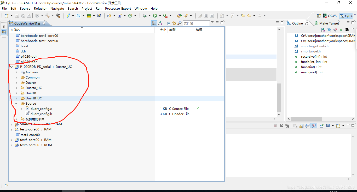
b. Modify the source - > DUART? Config. C file to define default? Freq 66 and change it to define default? Freq 100
c. build
d. Modify the link library of RAM project, right-click the project and click properties, open C / C + + general - > paths and symbols - > libraries, and change the path of uart1 ﹣ p1020rdb-pd.uc. A to the path of the library compiled by our project.
-
Rebuild the ram project, run debug, and check whether the serial port output is normal.
summary
Here we have to think about:
- What are the prerequisites for running linux on a chip? Or is it necessary to run RTOS? What are the prerequisites for running bare metal programs?
- This section is not only to verify DDR, but also to verify uart, because DDR can be verified in the previous DDR parameter verification.
- What does the tcl of SRAM and RAM do?
- Understanding of tcl files? For example, how to use tcl file to light led?

