Design of monocular endoscope positioning system based on FPGA (Part 2)
Today, we bring you the design of monocular endoscope positioning system based on FPGA. Due to the long length, it is divided into three parts. Today, I'll bring the third and second articles. I don't talk much and deliver the goods.
Reading guide
With the development of science and technology and the progress of society, information technology has developed rapidly. We can get a lot of information from the Internet, radio and other media. The storage, processing and transmission of modern information are becoming more and more digital. In people's daily life, all the commonly used computers, televisions, sound systems, video recording equipment and remote communication electronic equipment adopt electronic systems and digital circuit systems. Therefore, digital technology is more and more widely used. Especially in communication system and video system, digital system is particularly prominent. With the birth of FPGA, digital system is more favored by people. It provides a more convenient channel for the design of digital system, so that the digital system design can be miniaturized, the circuit scale is large, and the huge logic resources can meet the design of various digital systems.
With the development of society, science and technology have been applied in various fields, especially in the medical field. In the medical field, cardiac electrical signal simulator and surgical auxiliary instruments have developed rapidly. In order to train inexperienced doctors to be familiar with the operation process of heart surgery, special heart signal simulation instruments are developed to enable doctors to quickly master the operation process of heart surgery and become an experienced heart surgeon.
Therefore, based on the FPGA platform, this paper will use image processing combined with the principle of signal acquisition to realize the function that doctors can obtain the information of the catheter head in the heart without observing the internal situation of the heart during the operation of the catheter in cardiac simulation surgery, and use the endoscope camera to collect video and track and locate the catheter head, Signal acquisition technology can collect the signal of the catheter head touching the area inside the heart and send it to professional medical instruments for 3D modeling of the heart.
The realization of this design is very valuable for doctors with little experience to master the operation process of heart surgery as soon as possible. In the future, more medical graduates engaged in heart surgery or social doctors just engaged in this industry will be trained.
Abstract of the third part: this part will introduce the system debugging and testing and conclusions, including system resource performance debugging and analysis, system function test and other related contents, as well as the common resolution parameter table of VGA, overall circuit diagram, main program sharing and other appendices.
6, System debugging and testing
This design tests the performance and function of the system respectively. The performance test is to test the resource utilization and running speed of FPGA. The function test includes corrosion algorithm test, frame difference algorithm test, positioning function debugging and so on.
6.1 system resource performance commissioning and analysis
In this design, the resources used by FPGA are shown in Figure 6.1. The combined logic resources are 45%, the distributed register resources are 23%, the total logic macro unit is 52%, the memory unit is 15%, and a phase-locked loop is used. EP4CE6F17C8 has two PLLs in total, and the total resources used by logic macro units are less than 80%. Meet the requirements of design tasks.

Figure 6.1 EP4CE6F17C8 resource usage
The buffer module operates stably with a clock of 200M, which can be verified by the logic analyzer SigalTap. The verification results are shown in Fig. 6.2 and Fig. 6.3.

Figure 6.2 SDRAM transmission data diagram

Figure 6.3 SDRAM transmission data diagram
Conclusion: the designed buffer length is 512, the buffer node is 256, and 256 data are burst each time, as shown in Fig. 6.2 and Fig. 6.3. Within the effective signal range of data, the transmission data is correct. Moreover, the working clock runs at 200MHz, which can basically meet the needs of multi endpoint image data buffer.
6.2 system function test
Corrosion function test: before corrosion, many isolated noise points can be seen on the video output, and the output results are shown in Figure 6.4. After corrosion algorithm processing, the isolated noise points are significantly reduced, and the output results are shown in Figure 6.5.

Figure 6.4 image and frame difference results before corrosion

Figure 6.5 image and frame difference results after corrosion
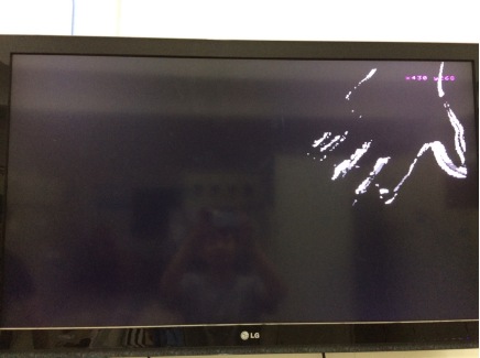
Figure 6.6 frame difference results
Frame difference debugging: the following problems and corresponding solutions are encountered in the debugging process.
Problem:
a. Move the screen, the image of the whole screen moves to the left, and the image is not distorted, as shown in Figure 6.6.
b. The result of frame difference is chaotic, as shown in Figure 6.6.
Analyze problems and solutions:
a. Cause analysis of the screen shifting problem: due to the SDRAM buffer reading and writing problem, when reading the previous frame, there is no time to read all the data, and the next frame image has arrived. The SDRAM writing priority is higher than the reading priority. Therefore, the next frame data will cover part of the data of the previous frame image, resulting in the deviation of the output image of each frame and screen shifting. Therefore, the solution is to adjust the reset delay parameter so that the write frame and read frame remain in the relationship of writing first and reading after a period of time delay.
b. Analysis on the causes of confusion of frame difference results: at the beginning, 16 bit RGB565 data was used for frame difference, and the results were shown in Fig. 6.6, resulting in confusion. Therefore, the use of synthetic image RGB565 for frame difference resulted in the overflow of the corresponding color subtraction of each channel to other channels, so the final subtraction result was confused. Therefore, the solution is to frame the gray image, subtract the two images, and then take the absolute value of the subtraction result (pay attention to prevent data overflow when subtracting and taking the absolute value), which is the correct frame difference result, as shown in figures 6.4 and 6.5. Observe that the edge contour of the two images is obvious, and there is an obvious tailing phenomenon.

Figure 6.7 moving target positioning

Figure 6.8 moving target positioning

Figure 6.9 moving target positioning
Function test results: the positioning is shown in Figure 6.7. With the movement of the target object, many coordinate points of the moving target object are output. According to the requirements of the design task, we only output the coordinates of the tail end of the target. The coordinates of the target to be captured are displayed in the upper right corner of the figure below. It can be seen that the position of the target is basically consistent with the output coordinates, as shown in Figure 6.7, Figure 6.8 and figure 6.9 show the positioning results of moving targets at different positions.
conclusion
In this paper, the implementation of frame difference algorithm, catheter head positioning and system performance are solved by the following means.
1. Ping pong operation will alternately store the images collected by the camera into two different SDRAM storage spaces. Through the buffer function of SDRAM, when VGA sends a request signal to SDRAM, read out the data of two adjacent frames at the same time, and then make frame difference.
2. The positioning of the catheter head is to determine the four boundaries of the moving target by projecting the image in the horizontal and vertical directions after the frame difference, and four coordinate points can be output. However, only one coordinate point is the endpoint of the catheter head, so calculate the distance between the intersection coordinates of the upper boundary and the moving object and the left and right boundaries, Judge whether the catheter head enters the camera vision from top left to bottom right or from bottom left to top right, determine the two-point coordinate output of the catheter, and then judge whether the remaining two-point coordinates are on the boundary of the whole image to determine the coordinate output of the catheter head.
3. This algorithm design uses more pipelining algorithms, and uses shift and splicing operations to replace multipliers and dividers, so as to improve the running speed of the system and reduce the utilization of resources.
Appendix a common resolution parameter table of VGA

Appendix B main codes
`include "../sdram_4port_ip/sdram_para.v"

module fd_target_location(
  ref_clk,
  rst_n,

  clk_out,

  //cmos interface
  CMOS_SCLK,    //cmos i2c clock
  CMOS_SDAT,    //cmos i2c data
  CMOS_VSYNC,    //cmos vsync
  CMOS_HREF,    //cmos hsync refrence
  CMOS_PCLK,    //cmos pxiel clock
  CMOS_XCLK,    //cmos externl clock
  CMOS_DB,    //cmos data

  //VGA port
  VGA_HSYNC,      //horizontal sync
  VGA_VSYNC,      //vertical sync
  VGAD,    //VGA data

  //SDRAM physical port
  S_CLK,
  S_CKE,
  S_NCS,
  S_NCAS,
  S_NRAS,
  S_NWE,
  S_BA,
  S_A,
  S_DB,
  S_DQM
);

  input ref_clk;
  input rst_n;

  output clk_out;

  //cmos interface
  output CMOS_SCLK;    //cmos i2c clock
  inout CMOS_SDAT;    //cmos i2c data
  input CMOS_VSYNC;    //cmos vsync
  input CMOS_HREF;    //cmos hsync refrence
  input CMOS_PCLK;    //cmos pxiel clock
  output CMOS_XCLK;    //cmos externl clock
  input  [7:0]  CMOS_DB;    //cmos data

  //VGA port
  output VGA_HSYNC;      //horizontal sync
  output VGA_VSYNC;      //vertical sync
  output  [15:0]  VGAD;    //VGA data

  //SDRAM physical port
  output S_CLK;
  output S_CKE;
  output S_NCS;
  output S_NCAS;
  output S_NRAS;
  output S_NWE;
  output [`BA-1:0] S_BA;
  output [`ROW-1:0] S_A;
  inout [`DQ-1:0] S_DB;
  output [`DQ/8-1:0] S_DQM;


assign clk_out = clk;
assign S_DQM = 0;

wire vga_clk, camera_clk, clk, sys_rst_n;
// wire rst_dly1, soft_rst_n;
wire soft_rst_0;
wire soft_rst_1;
wire soft_rst_2;
wire soft_rst_3;

wire Config_Done, sdram_init_done;
wire sys_we;
wire [15:0] sys_data_in;
wire frame_valid;
wire lcd_request;
wire [15:0] lcd_data_1;
wire [15:0] lcd_data_2;
wire [15:0] lcd_data;

wire sdram_wrreq;
wire sdram_wrval;
wire [`TOTAL_ADDR-1:0] sdram_wraddr;
wire [`DQ-1:0] sdram_wdata;
wire sdram_wdone;
wire sdram_rdreq;
wire sdram_rdval;
wire [`TOTAL_ADDR-1:0] sdram_rdaddr;
wire [`DQ-1:0] sdram_rdata;
wire sdram_rdone;
wire data_valid;

wire write_done_1;
wire read_done_1;
wire write_done_2;
wire read_done_2;


wire [23:0] waddr_min_1;
wire [23:0] waddr_max_1;

wire bound_valid;
wire [10:0] lcd_xpos;
wire [10:0] lcd_ypos;
wire [10:0] x_pos;
wire [10:0] y_pos;
wire lcd_val;
wire [15:0] lcd_dat;

wire start;
wire [11:0] bcd_x_pos;
wire [11:0] bcd_y_pos;
wire [10:0] target_x_pos;
wire [10:0] target_y_pos;
wire char_en;
wire [3:0] char_data;

reg dval_r1, dval_r2, dval_r3;


dcm dcm(
  .clk          (ref_clk),
  .rst_n          (rst_n),
  .soft_rst_0        (soft_rst_0),
  .soft_rst_1        (soft_rst_1),
  .soft_rst_2        (soft_rst_2),
  .soft_rst_3        (soft_rst_3),
  .clk_c0          (camera_clk), //camera configuration module clock output
  .clk_c1          (vga_clk), //vga module clock output
  .clk_c2          (clk), //sdram controller clock output
  .clk_c3          (S_CLK) //sdram port clock
);


I2C_AV_Config I2C_AV_Config
(
  /*Global clock*/
  .iCLK          (vga_clk),    //25MHz
  .iRST_N          (soft_rst_0),    //Global Reset


  .I2C_SCLK        (CMOS_SCLK),  //I2C CLOCK
  .I2C_SDAT        (CMOS_SDAT),  //I2C DATA

  .Config_Done      (Config_Done),//Config Done
  .LUT_INDEX        (),  //LUT Index
  .I2C_RDATA        ()  //I2C Read Data
);

CMOS_Capture
(
  /*Global Clock*/
  .iCLK          (camera_clk),      //13MHz
  .iRST_N          (soft_rst_2),

  /*I2C Initilize Done*/
  .Init_Done        (Config_Done & sdram_init_done),    //Init Done

  /*Sensor Interface*/
  .CMOS_RST_N        (),    //cmos work state(5ms delay for sccb config)
  .CMOS_PWDN        (),      //cmos power on
  .CMOS_XCLK        (CMOS_XCLK),    //
  .CMOS_PCLK        (CMOS_PCLK),    //25MHz
  .CMOS_iDATA        (CMOS_DB),    //CMOS Data
  .CMOS_VSYNC        (CMOS_VSYNC),    //L: Vaild
  .CMOS_HREF        (CMOS_HREF),    //H: Vaild

  /*Ouput Sensor Data*/
  .x_pos          (),
  .y_pos          (),
  .CMOS_HREF_pos      (),
  .CMOS_oCLK        (sys_we),    //1/2 PCLK
  .CMOS_oDATA        (sys_data_in),    //16Bits RGB
  .CMOS_VALID        (frame_valid),    //Data Enable
  .CMOS_FPS_DATA      ()  //cmos fps
);

wire corrode_dval_w1;
wire corrode_data_w1;
wire dilation_dval_w2;
wire dilation_data_w2;
wire dval_w2;
wire data_w2;
wire dval_w3;
wire [15:0] data_w3;

// image_smooth image_smooth(
  // .clk          (CMOS_PCLK),
  // .rst_n          (soft_rst_2),
  // .dval_i          (sys_we),
  // .data_i          (sys_data_in[7:0]),
  // .dval_o          (dval_1),
  // .data_o          (data_1)
// );

// median_filter median_filter(
  // .clk          (CMOS_PCLK),
  // .rst_n          (soft_rst_2),
  // .dval_i          (sys_we),
  // .data_i          (sys_data_in[7:0]),
  // .dval_o          (dval_1),
  // .data_o          (data_1)
// );

image_corrode image_corrode(
  .clk          (vga_clk),
  .rst_n          (soft_rst_3),
  .dval_i          (lcd_val),
  .data_i          (lcd_dat[0]),
  .dval_o          (corrode_dval_w1),
  .data_o          (corrode_data_w1)
);

image_dilation image_dilation(
  .clk          (vga_clk),
  .rst_n          (soft_rst_3),
  .dval_i          (corrode_dval_w1),
  .data_i          (corrode_data_w1),
  .dval_o          (dilation_dval_w2),
  .data_o          (dilation_data_w2)
);

//Binary image projection
projection projection(
  .clk          (vga_clk),
  .rst_n          (soft_rst_3),
  .dval_i          (lcd_val),
  .data_i          (lcd_dat[0]),
  .x_pos          (x_pos),
  .y_pos          (y_pos),
  .target_x_pos      (target_x_pos),
  .target_y_pos      (target_y_pos),
  .dval_o          (dval_w3),
  .data_o          (data_w3) //
);


bin_to_bcd u0_bin_to_bcd(.bin(target_x_pos), .bcd(bcd_x_pos));
bin_to_bcd u1_bin_to_bcd(.bin(target_y_pos), .bcd(bcd_y_pos));

char_mac u_char_mac(
  .clk        (vga_clk),
  .rst_n        (soft_rst_3),
  .start        (start),
  .bcd_x_pos      (bcd_x_pos),
  .bcd_y_pos      (bcd_y_pos),
  .char_en      (char_en),
  .char_data      (char_data)
);

char_disp u_char_disp
(
  .clk        (vga_clk),
  .rst_n        (soft_rst_3),
  .char_en      (char_en),
  .char_data      (char_data),
  .move_x_pos      (12'd560),
  .move_y_pos      (12'd30),
  .data_valid_pos    (start),
  .data_valid      (dval_w2), //dval_w2 lcd_val dval_w1 dilation_dval_w2
  .x_pos        (x_pos),
  .y_pos        (y_pos),
  .data_i        ({R[7:3], G[7:2], B[7:3]}), //{R[7:3], G[7:2], B[7:3]} lcd_dat {16{dilation_data_w2}} dilation_data_w2
  .data_valid_o    (),
  .data_o        (lcd_data)
);

//------------------------------------------------------
//Convert yuv to rgb output
wire [7:0] Y, Cb, Cr;
wire [7:0] R, G, B;
reg [15:0] data_r1;

yuv422_yuv444 yuv422_yuv444(
  .clk        (vga_clk),
  .rst_n        (soft_rst_3),
  .yuv_capture_en    (lcd_request), //ahead 2 clock
  .image_data      (lcd_data_1), //lcd_data_1
  .Y          (Y),
  .Cb          (Cb),
  .Cr          (Cr)
);

yuv2rgb yuv2rgb(
  .clk        (vga_clk),      //Clock input
  .rst        (soft_rst_3),      //Reset input
  .y_in        (Y),                   //Y-component output before transformation
  .cb_in        (Cb),                   //Cb component output before transformation
  .cr_in        (Cr),      //Cr component output before transformation
  .ena_in        (dval_r1),      //The data to be transformed is enabled. When it is high, the input data is valid
  .R_out        (R),      //Transformed R-component output
  .G_out        (G),      //G-component output after transformation
  .B_out        (B),      //Transformed B-component output
  .ena_out      (dval_w2)      //Data enable output after transformation
);


always @ (posedge vga_clk or negedge soft_rst_3)
  if(soft_rst_3 == 1'b0)
    dval_r1 <= 0;
  else dval_r1 <= lcd_request;

always @ (posedge vga_clk or negedge soft_rst_3)
  if(soft_rst_3 == 1'b0)
    dval_r2 <= 0;
  else dval_r2 <= dval_w2;

assign start = ~dval_r2 & dval_w2;


// Virtual_Camera Virtual_Camera(
  // .clk            (vga_clk),
  // .rst_n            (soft_rst_2),
  // .sdram_init_done      (sdram_init_done),
  // .dval            (sys_we),
  // .data            (sys_data_in)
// );

switch_in switch_in(
  .clk          (clk),
  .rst_n          (soft_rst_1),
  .frame_done        (write_done_1),
  .waddr_min_1      (waddr_min_1),
  .waddr_max_1      (waddr_max_1)
);

switch_out switch_out(
  .clk          (vga_clk),
  .rst_n          (soft_rst_3),
  .request        (lcd_request),
  .x_pos_i        (lcd_xpos),
  .y_pos_i        (lcd_ypos),
  .x_pos          (x_pos),
  .y_pos          (y_pos),
  .start_o        (),
  .lcd_data_1        (lcd_data_1),
  .lcd_data_2        (lcd_data_2),
  .lcd_val        (lcd_val),
  .lcd_data        (lcd_dat) //lcd_data
);


async_4fifo async_4fifo(
  .clk          (clk),
  .rst_n          (soft_rst_1),
  .sdram_init_done    (sdram_init_done), //sdram initialization completion signal

  /*User interface*/
  /*Write user 1 interface*/
  .clk_write_1      (CMOS_PCLK), //vga_clk, CMOS_PCLK
  .wrreq_1        (sys_we), //sys_we dval_1
  .wdata_1        (sys_data_in), //sys_data_in {8'd0, data_1}
  .write_done_1      (write_done_1),
  /*Parameter setting*/
  .waddr_min_1      (waddr_min_1), //24'd0
  .waddr_max_1      (waddr_max_1), //24'd307200
  .wr_length_1      (9'd256), //, this is the buffer node

  /*Read user 1 interface*/
  .clk_read_1        (vga_clk), //vga_clk
  .rdreq_1        (lcd_request), //lcd_request
  .rdata_1        (lcd_data_1), //lcd_data lcd_data_1
  .read_done_1      (),
  .data_valid_1      (data_valid), //sdram read port synchronization signal
  /*Parameter setting*/
  .raddr_min_1      (24'd0),
  .raddr_max_1      (24'd307200),
  .rd_length_1      (9'd256), //, this is the buffer node


  /*Write user 2 interface*/
  .clk_write_2      (CMOS_PCLK), //vga_clk, CMOS_PCLK
  .wrreq_2        (0), //sys_we
  .wdata_2        (0), //sys_data_in
  .write_done_2      (),
  /*Parameter setting*/
  .waddr_min_2      (24'd0), //24'd307200
  .waddr_max_2      (24'd0), //24'd614400
  .wr_length_2      (9'd256), //It is important to add a buffer node


  /*Read user 2 interface*/
  .clk_read_2        (vga_clk),
  .rdreq_2        (lcd_request), //lcd_request
  .rdata_2        (lcd_data_2), //lcd_data lcd_data_2
  .read_done_2      (),
  .data_valid_2      (data_valid), //sdram read port synchronization signal data_valid
  /*Parameter setting*/
  .raddr_min_2      (24'd307200), //24'd307200
  .raddr_max_2      (24'd614400), //24'd614400
  .rd_length_2      (9'd256), //It is important to add a buffer node


  /*Write SDRAM port*/
  .sdram_wrreq      (sdram_wrreq),
  .sdram_wrval      (sdram_wrval),
  .sdram_wraddr      (sdram_wraddr),
  .sdram_wdata      (sdram_wdata),
  .sdram_wdone      (sdram_wdone),

  /*Read SDRAM port*/
  .sdram_rdreq      (sdram_rdreq),
  .sdram_rdval      (sdram_rdval),
  .sdram_rdaddr      (sdram_rdaddr),
  .sdram_rdata      (sdram_rdata),
  .sdram_rdone      (sdram_rdone)
);


lsm_sdram lsm_sdram(
  /*global variable*/
  .clk          (clk),
  .rst_n          (soft_rst_1),
  .sdram_init_done    (sdram_init_done),

  /*Write SDRAM port*/
  .sdram_wrreq      (sdram_wrreq),
  .sdram_wrval      (sdram_wrval),
  .sdram_wraddr      (sdram_wraddr),
  .sdram_wdata      (sdram_wdata),
  .sdram_wdone      (sdram_wdone),

  /*Read SDRAM port*/
  .sdram_rdreq      (sdram_rdreq),
  .sdram_rdval      (sdram_rdval),
  .sdram_rdaddr      (sdram_rdaddr),
  .sdram_rdata      (sdram_rdata),
  .sdram_rdone      (sdram_rdone),

  /*SDRAM Physical port*/
  .sdram_clk        (),
  .sdram_cke        (S_CKE),
  .sdram_cs_n        (S_NCS),
  .sdram_cas_n      (S_NCAS),
  .sdram_ras_n      (S_NRAS),
  .sdram_we_n        (S_NWE),
  .sdram_ba        (S_BA),
  .sdram_a        (S_A),
  .sdram_dq        (S_DB),
  .sdram_dqm        ()
);


lcd_top lcd_top
(
  //global clock
  .clk          (vga_clk),      //system clock
  .rst_n          (soft_rst_3),         //sync reset

  //lcd interface
  .lcd_dclk        (),     //lcd pixel clock
  .lcd_blank        (),    //lcd blank
  .lcd_sync        (),    //lcd sync
  .lcd_hs          (VGA_HSYNC),        //lcd horizontal sync
  .lcd_vs          (VGA_VSYNC),        //lcd vertical sync
  .lcd_en          (),      //lcd display enable
  .lcd_rgb        (VGAD),    //lcd display data

  //user interface
  .lcd_request      (lcd_request),  //lcd data request
  .lcd_framesync      (data_valid),  //lcd frame sync
  .lcd_pos        (),
  .lcd_xpos        (lcd_xpos),    //lcd horizontal coordinate
  .lcd_ypos        (lcd_ypos),    //lcd vertical coordinate
  .lcd_data        (lcd_data)    //lcd data
);


endmodule
This is the end of this article. I'll see you later, great Xia!
[QQ communication group]
Group number: 173560979, group entry code: Jianghu fans of FPGA technology.
With many years of FPGA enterprise development experience, various easy to understand learning materials and methods, and a strong exchange and learning atmosphere, QQ group has more than 1000 like-minded partners. There is no advertising pure mode, which provides a pure land for technical exchange, from novice Xiaobai to elite industry leaders, from military industry to civil enterprises, from communication It has everything from image processing to artificial intelligence.
[wechat communication group]
Now WeChat communication group has established 09 groups, with a total of thousands of people. Welcome to pay attention to the WeChat official account of FPGA technology, and get access to the group.
finish
The follow-up will be continuously updated, bringing installation related design tutorials such as Vivado, ISE, Quartus II and candence, learning resources, project resources, good article recommendations, etc. I hope you will continue to pay attention.
The Jianghu is so big. Continue to wander. I wish you all the best. Goodbye!