Today, we bring you the design of real-time image edge detection system based on FPGA. Due to the long length, it is divided into three parts. Today, I'll bring the third and second articles. I don't talk much and deliver the goods.
Reading guide
With the rapid development of science and technology, FPGA brings new opportunities for digital image processing in system structure. The information in the image exists in parallel, so the same operation can be performed on it in parallel, which greatly improves the speed of image processing, which is just suitable for mapping to FPGA architecture and realizing it with hardware algorithm.
This paper describes the design idea and process of a digital image processing system based on FPGA, which can collect, process and display in real time, and analyzes the timing of camera interface; The capture principle of image information is described; The functions of each module of image edge detection are introduced in detail; This paper focuses on the design of median filter module with denoising function; The selection of edge detection operator is briefly described; The working principle and control mode of SDRAM are systematically introduced; VGA timing is introduced; Finally, the whole system is verified and summarized, including the verification of simulation waveform and board level verification.
Based on the solid FPGA development board, the system realizes the real-time acquisition, real-time edge detection and real-time display of image data. It runs stably and has high real-time performance, which also shows that FPGA does have the ability of massive data high-speed transmission.
This article is the collation of my graduation project in that year. You heroes can read and learn according to your own needs.
The third content summary: this chapter will introduce the system verification, conclusion and the main codes of each module, including the main codes of image real-time acquisition module, image real-time capture module, median filter module, edge detection module, image cache module and image real-time display module.
5, System verification
In the design process of this system, I mainly use the top-down hierarchical design idea to design the top-level architecture of the system, clarify the functions of each module and the handshake relationship between each module, then write and verify the code by module, debug the code to realize the functions of each module, and finally conduct simulation verification based on the top-level module, As shown in figures 5-1 and 5-2, the simulation waveforms of the top-level module of the system are shown, in which figure 5-1 is the global waveform and Figure 5-2 is the locally amplified waveform.
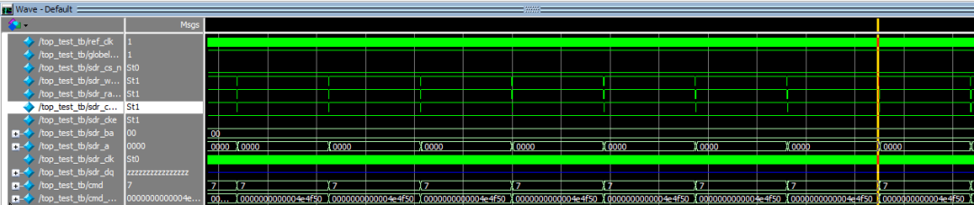
Figure 5-1 global simulation waveform of system top-level module
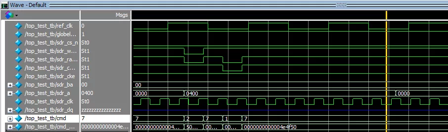
Figure 5-2 local simulation waveform of the top module of the system
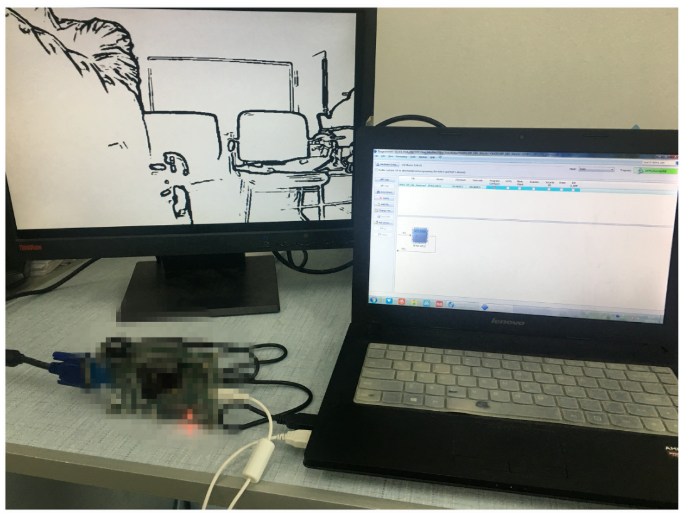
Then connect the FPGA development experimental board and update its driver, allocate pins according to the configuration file of the development board, and conduct board level test after the full compilation. The development board used in the verification of this system is the physical FPGA development board.
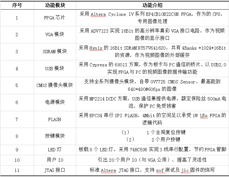
The entity FPGA development board adopts the EP4CE10E22C8N chip of Altera Cyclone IV series. The development board is an FPGA image development board. Its core chip EP4CE10E22C8N has 6272 logic units and 150 IO pins. The development board is equipped with VGA, USB, CMOS interface, SDRAM, keys, LED and many other external devices, which can be used as hardware tools for the design and verification of the system.
The main parameters of the entity FPGA development board are shown in table 6-1 below.
Table 5-1 main parameters of FPGA development board
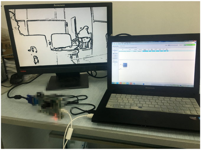
The results of the lower board show that the function of the digital image edge detection system I designed has been realized, which can collect images in real time, process and display them in real time. What is intercepted here is pictures, and the real scene display can be displayed in real time according to the movement of the camera.
6, Conclusion
In the design of this system, the main equipment driven by FPGA is as follows: the camera model is Ov7725; Universal VGA interface. At the same time, I studied the relevant edge detection algorithms. In order to make the data processing results more accurate, I also preprocessed the image data according to the needs of the system: first convert the color image into gray file; Then, the median filter technology is used to denoise the collected image data effectively. Through the design of this system, I deeply understand the basic principle of driving external devices based on FPGA, master the ability of driving external devices and implementing algorithms based on FPGA and Verilog language, feel the advancement of FPGA, and further determine my own development direction. During the system verification, the real-time acquisition, real-time edge detection and real-time display of image data are realized based on FPGA development board. The system has good performance and high real-time performance. The results show that FPGA can easily realize the high-speed transmission of massive data.
Attachment: some main codes
Main code of image real-time acquisition module:
1 module sccb_config_ctrl(
2 clk, //24Mhz input clock
3 rst_n, //System reset
4 scl, //iic clock line
5 sda, //iic data line
6 config_done //Configuration completion flag
7 );
8 //System input
9 input clk; //External input clock 24Mhz
10 input rst_n; //System reset
11 //system output
12 output reg scl; //iic clock line
13 output reg config_done; //Configuration completion flag
14
15
16 inout sda; //iic data line
17
18 reg sda_buffer; //Intermediate register for writing data
19 reg flag; //Does the control system have bus control
20 reg [7:0] lut_cnt; //Pointer register counter
21 reg [15:0] lut_data; //Register address and configuration data
22 reg [3:0] s;
23
24 assign sda = (flag) ? sda_buffer : 1'bz;//When the flag is high, the system has bus control
25 //And send SDA_ Data in buffer. When the flag is low,
26 //Release the bus.
27
28 //----------Delay 1ms counter-----------------
29 reg [31:0] delay_cnt;
30 reg delay_done;
31
32 always @ (posedge clk or negedge rst_n)
33 begin
34 if(!rst_n)
35 begin
36 delay_done <= 0;
37 delay_cnt <= 0;
38 end
39 else if(delay_cnt == 20000) //23809
40 delay_done <= 1;
41 else
42 begin
43 delay_cnt <= delay_cnt + 1;
44 delay_done <= 0;
45 end
46 end
47
48 //----------------Frequency division generates 400Khz clock clk_sys----------
49 reg [7:0] count;//Counter
50 reg clk_sys;//System clock
51 reg [5:0] state;//Status register
52
53 always @ (posedge clk or negedge rst_n)
54 begin
55 if (!rst_n)
56 begin
57 clk_sys <= 1'b1;
58 count <= 8'd0;
59 end
60 else
61 if (count < 100)//Frequency division becomes a clock of nearly 200K
62 count <= count + 1;
63 else
64 begin
65 count <= 8'd0;
66 clk_sys <= ~clk_sys;
67 end
68 end
69
70 //------------------Output scl-------------
71 always @ (negedge clk_sys or negedge rst_n)
72 begin
73 if (!rst_n)
74 begin
75 scl <= 1'b1;//When reset, scl is high
76 end
77 else
78 begin
79 if(config_done == 1 || delay_done == 0)//When the bus is busy, scl is a clock of nearly 400K
80 scl <= 1;
81 else
82 scl <= ~scl;//When idle, scl is high
83 end
84 end
85
86 reg [3:0] cnt;//Number of data sent or received
87 reg [15:0] memory;//An intermediate register that sends or receives data
88
89 always @ (posedge clk_sys or negedge rst_n)
90 begin
91 if (!rst_n)
92 begin
93 config_done <= 0;
94 flag <= 1'b1; //When reset, the system obtains control of the bus
95 sda_buffer <= 1'b1; //Send high level to the data line of iic
96 state <= 0;
97 cnt <= 0;
98 memory <= 16'd0;
99 lut_cnt <= 2;
100 s <= 0;
101 end
102 else
103 case(state)
104 0 :if(scl)
105 begin
106 if(delay_done)//Delay flag signal pulled high
107 begin
108 sda_buffer <= 1'b0; //Send start signal
109 state <= 1;
110 memory <= 16'h0042;//Prepare ID address
111 end
112 else
113 state <= 0;
114 end
115 else
116 state <= 0;
117
118 1 :if((scl == 0) && (cnt < 8))//Send ID address
119 begin
120 sda_buffer <= memory[7];
121 cnt <= cnt + 1;
122 memory = {memory[14:0],memory[15]};
123 state <= 1;
124 end
125 else
126 begin
127 if ((scl == 0) && (cnt == 8))
128 begin
129 cnt <= 0;
130 flag <= 0;//Release bus control
131 state <= 2;
132 end
133 else
134 begin
135 state <= 1;
136 end
137 end
138
139 2 :
140 if(scl)//Receive data during SCL high level
141 begin
142 if(!sda)//Detection response signal
143 begin
144 state <= 3;
145 memory <= lut_data;//Pointer register address
146 end
147 else
148 begin
149 state <= 0;
150 end
151 end
152 else
153 state <= 2;
154
155 3 : if((scl == 0) && (cnt < 8)) //Send pointer register address
156 begin
157 flag <= 1;//Gain bus control
158 sda_buffer <= memory[15];
159 cnt <= cnt + 1;
160 memory = {memory[14:0],memory[15]};
161 state <= 3;
162 end
163 else
164 begin
165 if ((scl == 0) && (cnt == 8))
166 begin
167 cnt <= 0;
168 flag <= 0;//Release bus control
169 state <= 4;
170 end
171 else
172 begin
173 state <= 3;
174 end
175 end
176
177 4 :
178 if(scl)
179 begin
180 if(!sda)//Detection response signal
181 begin
182 state <= 5;
183 end
184 else
185 begin
186 state <= 0;
187 end
188 end
189
190 5 : if((scl == 0) && (cnt < 8))//Send octet control word
191 begin
192 flag <= 1; //Gain bus control
193 sda_buffer <= memory[15];
194 cnt <= cnt + 1;
195 memory <= {memory[14:0],memory[15]};
196 state <= 5;
197 end
198 else
199 begin
200 if ((scl == 0) && (cnt == 8))
201 begin
202 cnt <= 0;
203 flag <= 0; //Release bus control
204 state <= 6;
205 lut_cnt <= lut_cnt + 1; //Register pointer + 1
206 end
207 else
208 begin
209 state <= 5;
210 end
211 end
212
213 6 :
214 if(scl) //Receive ACK during SCL high level
215 begin
216 if(!sda)//Detection response signal
217 begin
218 state <= 7;
219 end
220 else
221 begin
222 state <= 0;
223 end
224 end
225
226 7 : if (scl == 0)
227 begin
228 flag <= 1;
229 sda_buffer <= 0;//Pull down the data cable (prepare for sending stop signal)
230 state <= 8;
231 end
232 else
233 state <= 7;
234
235 8 : if (scl == 1) //Send stop signal
236 begin
237 sda_buffer <= 1;
238 begin
239 if (s == 8)
240 begin
241 if(lut_cnt < 70)
242 begin
243 state <= 0;
244 s <= 0;
245 end
246 else
247 config_done <= 1; //Configuration complete
248 end
249 else
250 s <= s + 1;
251 end
252 end
253 else
254 state <= 8;
255
256 default : state <= 0;
257 endcase
258 end
259
260 always @ (*)
261 begin
262 case (lut_cnt)
263 // OV7725 : VGA RGB565 Config
264 //Read Data Index
265 // 0 : LUT_DATA = {8'h0A, 8'h77}; //Product ID Number MSB (Read only)
266 // 1 : LUT_DATA = {8'h0B, 8'h21}; //Product ID Number LSB (Read only)
267 0 : lut_data = {8'h1C, 8'h7F}; //Manufacturer ID Byte - High (Read only)
268 1 : lut_data = {8'h1D, 8'hA2}; //Manufacturer ID Byte - Low (Read only)
269 //Write Data Index
270 2 : lut_data = {8'h12, 8'h80}; // BIT[7]-Reset all the Reg
271 3 : lut_data = {8'h3d, 8'h03}; //DC offset for analog process
272 4 : lut_data = {8'h15, 8'h02}; //COM10: href/vsync/pclk/data reverse(Vsync H valid)
273 5 : lut_data = {8'h17, 8'h22}; //VGA: 8'h22; QVGA: 8'h3f;
274 6 : lut_data = {8'h18, 8'ha4}; //VGA: 8'ha4; QVGA: 8'h50;
275 7 : lut_data = {8'h19, 8'h07}; //VGA: 8'h07; QVGA: 8'h03;
276 8 : lut_data = {8'h1a, 8'hf0}; //VGA: 8'hf0; QVGA: 8'h78;
277 9 : lut_data = {8'h32, 8'h00}; //HREF / 8'h80
278 10 : lut_data = {8'h29, 8'hA0}; //VGA: 8'hA0; QVGA: 8'hF0
279 11 : lut_data = {8'h2C, 8'hF0}; //VGA: 8'hF0; QVGA: 8'h78
280 //If the internal PLL is not used, this command is invalid
281 12 : lut_data = {8'h0d, 8'h41}; //Bypass PLL 00:0 01:4x 10:6x 11:8x
282 13 : lut_data = {8'h11, 8'h01}; //CLKRC,Finternal clock = Finput clk*PLL multiplier/[(CLKRC[5:0]+1)*2] = 25MHz*4/[(x+1)*2]
283 //00: 50fps, 01:25fps, 03:12.5fps (50Hz Fliter)
284 14 : lut_data = {8'h12, 8'h06}; //BIT[6]: 0:VGA; 1;QVGA
285 //BIT[3:2]: 01:RGB565
286 //VGA: 00:YUV; 01:Processed Bayer RGB; 10:RGB; 11:Bayer RAW; BIT[7]-Reset all the Reg
287 15 : lut_data = {8'h0C, 8'h10}; //COM3: Bit[7:6]:Vertical/Horizontal mirror image ON/OFF, Bit[0]:Color bar; Default:8'h10
288 //DSP control
289 16 : lut_data = {8'h42, 8'h7f}; //BLC Blue Channel Target Value, Default: 8'h80
290 17 : lut_data = {8'h4d, 8'h09}; //BLC Red Channel Target Value, Default: 8'h80
291 18 : lut_data = {8'h63, 8'hf0}; //AWB Control
292 19 : lut_data = {8'h64, 8'hff}; //DSP_Ctrl1:
293 20 : lut_data = {8'h65, 8'h00}; //DSP_Ctrl2:
294 21 : lut_data = {8'h66, 8'h00}; //{COM3[4](0x0C), DSP_Ctrl3[7]}:00:YUYV; 01:YVYU; [10:UYVY] 11:VYUY
295 22 : lut_data = {8'h67, 8'h00}; //DSP_Ctrl4:00/01: YUV or RGB; 10: RAW8; 11: RAW10
296 //AGC AEC AWB
297 23 : lut_data = {8'h13, 8'hff};
298 24 : lut_data = {8'h0f, 8'hc5};
299 25 : lut_data = {8'h14, 8'h11};
300 26 : lut_data = {8'h22, 8'h98}; //Banding Filt er Minimum AEC Value; Default: 8'h09
301 27 : lut_data = {8'h23, 8'h03}; //Banding Filter Maximum Step
302 28 : lut_data = {8'h24, 8'h40}; //AGC/AEC - Stable Operating Region (Upper Limit)
303 29 : lut_data = {8'h25, 8'h30}; //AGC/AEC - Stable Operating Region (Lower Limit)
304 30 : lut_data = {8'h26, 8'ha1}; //AGC/AEC Fast Mode Operating Region
305 31 : lut_data = {8'h2b, 8'h9e}; //TaiWan: 8'h00:60Hz Filter; Mainland: 8'h9e:50Hz Filter
306 32 : lut_data = {8'h6b, 8'haa}; //AWB Control 3
307 33 : lut_data = {8'h13, 8'hff}; //8'hff: AGC AEC AWB Enable; 8'hf0: AGC AEC AWB Disable;
308 //matrix sharpness brightness contrast UV
309 34 : lut_data = {8'h90, 8'h0a};
310 35 : lut_data = {8'h91, 8'h01};
311 36 : lut_data = {8'h92, 8'h01};
312 37 : lut_data = {8'h93, 8'h01};
313 38 : lut_data = {8'h94, 8'h5f};
314 39 : lut_data = {8'h95, 8'h53};
315 40 : lut_data = {8'h96, 8'h11};
316 41 : lut_data = {8'h97, 8'h1a};
317 42 : lut_data = {8'h98, 8'h3d};
318 43 : lut_data = {8'h99, 8'h5a};
319 44 : lut_data = {8'h9a, 8'h1e};
320 45 : lut_data = {8'h9b, 8'h3f}; //Brightness
321 46 : lut_data = {8'h9c, 8'h25};
322 47 : lut_data = {8'h9e, 8'h81};
323 48 : lut_data = {8'ha6, 8'h06};
324 49 : lut_data = {8'ha7, 8'h65};
325 50 : lut_data = {8'ha8, 8'h65};
326 51 : lut_data = {8'ha9, 8'h80};
327 52 : lut_data = {8'haa, 8'h80};
328 //Gamma correction
329 53 : lut_data = {8'h7e, 8'h0c};
330 54 : lut_data = {8'h7f, 8'h16}; //
331 55 : lut_data = {8'h80, 8'h2a};
332 56 : lut_data = {8'h81, 8'h4e};
333 57 : lut_data = {8'h82, 8'h61};
334 58 : lut_data = {8'h83, 8'h6f};
335 59 : lut_data = {8'h84, 8'h7b};
336 60 : lut_data = {8'h85, 8'h86};
337 61 : lut_data = {8'h86, 8'h8e};
338 62 : lut_data = {8'h87, 8'h97};
339 63 : lut_data = {8'h88, 8'ha4};
340 64 : lut_data = {8'h89, 8'haf};
341 65 : lut_data = {8'h8a, 8'hc5};
342 66 : lut_data = {8'h8b, 8'hd7};
343 67 : lut_data = {8'h8c, 8'he8};
344 68 : lut_data = {8'h8d, 8'h20};
345 //Others
346 69 : lut_data = {8'h0e, 8'h65};//night mode auto frame rate control
347 default : lut_data = {8'h1C, 8'h7F};
348 endcase
349 end
350
351 endmodule
Main code of image real-time capture module:
1  module coms_capture_rgb565(clk_cmos, rst_n, pclk, vsync, href, din, xclk,
2       frame_data, frame_clk, frame_href, frame_vsync, cmos_fps_rate);
3
4   input clk_cmos; //24Mhz drive clock input
5   input rst_n;
6   input pclk;      //Input pixel clock
7   input vsync;     //Input field synchronization signal
8   input href;      //Input line synchronization signal
9   input [7:0] din; //Input pixel data
10
11  output xclk;        //The output CMOS Sensor's drive clock is 0.24Mhz
12  output frame_clk; //Clock for outputting pixel data after splicing
13  output [15:0] frame_data;  //Output pixel data after splicing
14  output frame_href;   //Output synchronized line synchronization signal
15  output frame_vsync;  //Output synchronous field synchronization signal
16  output reg cmos_fps_rate;  //Output frame rate
17
18  assign xclk = clk_cmos;
19
20  //-------------Detect field and line synchronization signals------------
21  reg href_r, vsync_r;
22  always @(posedge pclk or negedge rst_n)
23  begin
24      if (!rst_n)
25          begin
26              href_r <= 1;
27              vsync_r <= 1;
28          end
29      else
30          begin
31              href_r <= href;
32              vsync_r <= vsync;
33          end
34  end
35  //The line synchronization signal changes from low level to high level, indicating that the data is valid
36  assign pose_href = (~href_r) & href;
37  //The field synchronization signal changes from high level to low level, indicating that one frame of data has been received
38  assign nege_vsync = vsync_r & (~vsync);
39
40  //----------A flag number is generated by delaying 10 frames----------
41  reg frame_cnt_end; //Delayed 10 frame data end flag
42  reg [3:0] frame_cnt;         //Frame counter
43  always @(posedge pclk or negedge rst_n)
44  begin
45      if(!rst_n)
46          begin
47              frame_cnt <= 0;
48              frame_cnt_end <= 0;
49          end
50      else if (frame_cnt == 10)
51          frame_cnt_end <= 1;
52      else if(nege_vsync)
53          frame_cnt <= frame_cnt + 1;
54      else
55          frame_cnt <= frame_cnt;
56  end
57
58  reg [15:0] din_buffer2;
59  reg [7:0] din_buffer1;
60  reg byte_flag;
61  reg [10:0] cnt;
62  always @(posedge pclk or negedge rst_n)
63  begin
64      if(!rst_n)
65          begin
66              byte_flag <= 0;
67              din_buffer1 <= 0;
68              din_buffer2 <= 0;
69              cnt <= 0;
70          end
71      else if(href)
72          begin
73              cnt <= cnt  + 1;
74              din_buffer1 <= din;
75              if(cnt >= 1278)
76                  byte_flag <= 0;
77              else
78                  byte_flag <= ~byte_flag;
79
80              if(byte_flag == 1)
81                  din_buffer2 <= {din_buffer1,din};
82              else
83                  din_buffer2 <= din_buffer2;
84          end
85      else
86          begin
87              byte_flag <= 0;
88              din_buffer1 <= 0;
89              din_buffer2 <= din_buffer2;
90              cnt <= 0;
91          end
92  end
93
94  reg byte_flag_r;
95  always@(posedge pclk or negedge rst_n)
96  begin
97      if(!rst_n)
98          byte_flag_r <= 0;
99      else
100         byte_flag_r <= byte_flag;
101 end
102
103 assign frame_data = frame_cnt_end & href ? din_buffer2 : 0;
104 assign frame_clk = frame_cnt_end ? byte_flag_r : 0;
105 assign frame_vsync = frame_cnt_end ? vsync_r : 1'b0;
106 assign frame_href = frame_cnt_end ? href_r : 1'b0;
107
108 reg [27:0] delay_cnt;
109 always@(posedge pclk or negedge rst_n)
110 begin
111     if(!rst_n)
112         delay_cnt <= 0;
113     else if(delay_cnt < 48000000 - 1'b1)
114         delay_cnt <= delay_cnt + 1'b1;
115     else
116         delay_cnt <= 0;
117 end
118 wire    delay_2s = (delay_cnt == 48000000 - 1'b1) ? 1'b1 : 1'b0;
119
120 reg [8:0] cmos_fps_cnt;
121 always @(posedge pclk or negedge rst_n)
122 begin
123     if(!rst_n)
124         begin
125             cmos_fps_cnt <= 0;
126             cmos_fps_rate <= 0;
127         end
128     else if(delay_2s == 1'b0)
129         begin
130             cmos_fps_cnt <= nege_vsync ? cmos_fps_cnt + 1'b1 : cmos_fps_cnt;
131             cmos_fps_rate <= cmos_fps_rate;
132         end
133     else
134         begin
135             cmos_fps_cnt <= 0;
136             cmos_fps_rate <= cmos_fps_cnt[8:1];
137         end
138 end
139
140 endmodule
Main code of median filter module:
1  module zhongzhilvbo (clk, rst_n, data_in, fifo_empty, data_out, wrreq, rdreq);
2
3   input clk;
4   input rst_n;
5   input [23:0] data_in;
6   input fifo_empty;
7
8   output [7:0] data_out;
9   output reg wrreq;
10  output reg rdreq;
11
12  reg [7:0] data [8:0];
13  wire [7:0] data_n[8:0];
14  reg shift;
15
16  assign data_out = data_n[4];
17
18  always @ (posedge clk or negedge rst_n)
19      begin
20          if (!rst_n)
21              begin
22                  data [8] <= 0;
23                  data [7] <= 0;
24                  data [6] <= 0;
25                  data [5] <= 0;
26                  data [4] <= 0;
27                  data [3] <= 0;
28                  data [2] <= 0;
29                  data [1] <= 0;
30                  data [0] <= 0;
31              end
32          else
33              begin
34                  if (shift)
35                      begin
36                          data[8] <= data[5];
37                          data[7] <= data[4];
38                          data[6] <= data[3];
39                          data[5] <= data[2];
40                          data[4] <= data[1];
41                          data[3] <= data[0];
42                          data[2] <= data_in[23:16];
43                          data[1] <= data_in[15:8];
44                          data[0] <= data_in[7:0];
45                      end
46              end
47      end
48
49  reg compara_rst_n;
50  genvar i;
51  reg [7:0] temp;
52  reg temp_rst_n;
53  reg [3:0] count;
54
55  always @ (posedge clk or negedge temp_rst_n)
56      begin
57          if (!temp_rst_n)
58              begin
59                  temp <= data [8];
60                  count <= 0;
61              end
62          else
63              begin
64                  temp <= data[count];
65                  count <= count + 1;
66              end
67
68      end
69  generate
70      for (i = 0; i < 9; i = i + 1)
71          begin : compara
72              if (i == 0)
73                  begin
74                      comparaer u1(.clk(clk), .rst_n(compara_rst_n), .ex_data(temp), .up_data(8'hff), .self_data(data_n[i]));
75                  end
76              else
77                  begin
78                      comparaer comparaer(.clk(clk), .rst_n(compara_rst_n), .ex_data(temp), .up_data(data_n[i-1]), .self_data(data_n[i]));
79                  end
80          end
81  endgenerate
82
83  reg [2:0] state;
84  reg [3:0] cnt;
85
86  always @ (posedge clk or negedge rst_n)
87      begin
88          if (!rst_n)
89              begin
90                  rdreq <= 0;
91                  compara_rst_n <= 0;
92                  wrreq <= 0;
93                  state <= 0;
94                  shift <= 0;
95                  cnt <= 0;
96                  temp_rst_n <= 0;
97              end
98          else
99              begin
100                 case (state)
101                     0 : begin
102                             if (fifo_empty)
103                                 begin
104                                     state <= 0;
105                                     wrreq <= 0;
106                                     compara_rst_n <= 0;
107                                 end
108                             else
109                                 begin
110                                     state <= 1;
111                                     rdreq <= 1;
112                                     wrreq <= 0;
113                                     compara_rst_n <= 0;
114                                 end
115                         end
116
117                     1 : begin
118                             rdreq <= 0;
119                             shift <= 1;
120                             state <= 2;
121                         end
122
123                     2 : begin
124                             shift <= 0;
125                             temp_rst_n <= 1;
126                             state <= 3;
127                         end
128
129                     3 : begin
130                             if (cnt < 8)
131                                 begin
132                                     cnt <= cnt + 1;
133                                     compara_rst_n <= 1;
134                                     state <= 3;
135                                 end
136                             else
137                                 begin
138                                     cnt <= 0;
139                                     temp_rst_n <= 0;
140                                     state <= 4;
141                                 end
142                         end
143
144                     4 : begin
145                             wrreq <= 1;
146                             state <= 0;
147                         end
148
149                 endcase
150             end
151     end
152 endmodule
Main code of edge detection module:
1  module sob (clk, rst_n, data, result, fifo_wr, shift_en);
2
3   input clk;
4   input rst_n;
5   input [23:0] data;
6   input shift_en;
7
8   output reg [7:0] result;
9   output reg fifo_wr;
10
11
12  reg [7:0]   O[-1:1][-1:1];
13  reg signed  [10:0]  Dx, Dy;
14
15  function [10:0] abs ( input signed [10:0] x);
16      abs = x >=0 ? x : -x ;        //Take the absolute value of x
17  endfunction
18
19  always @ (posedge clk or negedge rst_n)
20      begin
21          if (!rst_n)
22              begin
23                  result <= 8'd0;
24                  Dx <= 0;
25                  Dy <= 0;
26              end
27          else
28              begin
29                  if ( shift_en )
30                      begin
31                          result <= (abs(Dx) + abs(Dy))>>3 ;//Shift three bits to the right to divide by 8
32                          Dx  <= -$signed({3'b000, O[-1][-1]})    //-1* O[-1][-1]
33                                  +$signed({3'b000, O[-1][+1]})   //+1* O[-1][+1]
34                                  -($signed({3'b000, O[ 0][-1]})  //-2* O[ 0][-1]
35                                  <<1)
36                                  +($signed({3'b000, O[ 0][+1]})  //+2* O[ 0][+1]
37                                  <<1)
38                                  -$signed({3'b000, O[+1][-1]})   //-1* O[+1][-1]
39                                  +$signed({3'b000, O[+1][+1]});  //+1* O[+1][+1]
40                          Dy  <= $signed({3'b000, O[-1][-1]}) //+1* O[-1][-1]
41                                  +($signed({3'b000, O[-1][ 0]})  //+2* O[-1][0]
42                                  <<1)
43                                  +$signed({3'b000, O[-1][+1]})   //+1* O[-1][+1]
44                                  -$signed({3'b000, O[+1][-1]})//-1* O[+1][-1]
45                                  -($signed({3'b000, O[+1][ 0]})  //-2* O[+1][ 0]
46                                  <<1)
47                                  -$signed({3'b000, O[+1][+1]});  //-1* O[+1][+1]
48                          O[-1][-1]   <=  O[-1][0];
49                          O[-1][ 0]   <=  O[-1][+1];
50                          O[-1][+1]   <=  data[23:16];
51                          O[ 0][-1]   <=  O[0][0];
52                          O[ 0][ 0]   <=  O[0][+1];
53                          O[ 0][+1]   <=  data[15:8];
54                          O[+1][-1]   <=  O[+1][0];
55                          O[+1][ 0]   <=  O[+1][+1];
56                          O[+1][+1]   <=  data[7:0];
57              end
58          end
59      end
60
61
62
63  reg [2:0] state;
64
65  always @ (posedge clk or negedge rst_n)
66      begin
67          if (!rst_n)
68              begin
69                  fifo_wr <= 1'b0;
70                  state <= 0;
71              end
72          else
73              begin
74                  case (state)
75                      0 : begin
76                              if (shift_en)
77                                  begin
78                                      state <= 2;
79                                      fifo_wr <= 0;
80                                  end
81                              else
82                                  begin
83                                      state <= 0;
84                                      fifo_wr <= 0;
85                                  end
86                      end
87
88                      1 : begin
89                                  if (shift_en)
90                                      begin
91                                          fifo_wr <= 1'b1;
92                                      end
93                                  else
94                                      fifo_wr <= 0;
95                          end
96
97                      2 : state <= 3;
98
99                      3 : state <= 4;
100
101                     4 : state <= 1;
102
103                     default : state <= 0;
104
105                 endcase
106             end
107     end
108
109 endmodule
Main code of image cache module:
1  `include "sdram_head.v"
2
3  module sdr_fsm(soft_rst_n, sys_clk, init_done, ref_done, rd_done, wr_done, ref_time, mux_sel,
4           init_rst_n, ref_rst_n, rd_rst_n, wr_rst_n, time_rst_n, int_addr,
5            local_rdreq, local_wrreq, local_ready,wr_ddr,rd_ddr,rd_finish, wr_finish,local_finish);
6
7   input soft_rst_n;
8   input sys_clk;
9   input init_done;
10  input ref_done;
11  input rd_done;
12  input wr_done;
13  input [9:0] ref_time;
14  input [24:0] wr_ddr;
15  input [24:0] rd_ddr;
16
17 //   input [24:0] local_addr;
18 //   output reg [31:0] local_rdata;
19 //   input [31:0] local_wdata;
20  input local_rdreq, local_wrreq;
21  output reg local_ready,local_finish;
22  output reg rd_finish;
23  output reg wr_finish;
24
25  output reg [1:0] mux_sel;
26  output reg init_rst_n;
27  output reg ref_rst_n;
28  output reg rd_rst_n;
29  output reg wr_rst_n;
30  output reg time_rst_n;
31 //   output reg [31:0] wr_data;
32  output reg [24:0] int_addr;
33
34  localparam s0 = 3'b000;
35  localparam s1 = 3'b001;
36  localparam s2 = 3'b010;
37  localparam s3 = 3'b011;
38  localparam s4 = 3'b100;
39
40  reg [2:0] state;
41
42  reg rd,rd_en;
43
44  always @ (posedge sys_clk)
45      begin
46          if (!soft_rst_n)
47              begin
48                  rd <= 0;
49              end
50          else
51              begin
52                  if (local_rdreq && rd_en)
53                      rd <= local_rdreq;
54                  else
55                      if (!rd_en)
56                          rd <= 0;
57                      else
58                          rd <= rd;
59              end
60      end
61
62      reg wr,wr_en;
63
64  always @ (posedge sys_clk)
65      begin
66          if (!soft_rst_n)
67              begin
68                  wr <= 0;
69              end
70          else
71              begin
72                  if (local_wrreq && wr_en)
73                      wr <= local_wrreq;
74                  else
75                      if (!wr_en)
76                          wr <= 0;
77                      else
78                          wr <= wr;
79              end
80      end
81
82
83  always @ (posedge sys_clk)
84  begin
85      if (!soft_rst_n)
86          begin
87              mux_sel <= `INIT;
88              init_rst_n <= 0;
89              ref_rst_n <= 0;
90              wr_rst_n <= 0;
91              rd_rst_n <= 0;
92              time_rst_n <= 0;
93              state <= s0;
94 //               local_rdata <= 32'd0;
95              local_ready <= 0;
96              rd_finish <= 0;
97              wr_finish <= 0;
98 //               wr_data <= 32'd0;
99              int_addr <= 25'd0;
100             wr_en <= 1;
101             rd_en <= 1;
102             local_finish <= 0;
103         end
104     else
105         case (state)
106         s0 :  if (!init_done)
107                     init_rst_n <= 1;
108                 else
109                     begin
110                         init_rst_n <= 0;
111                         mux_sel <= `REF;
112                         time_rst_n <= 1;
113                         state <= s1;
114                         local_ready <= 1;
115                         wr_en <= 1;
116                         rd_en <= 1;
117                     end
118
119         s1 :  if ((ref_time < `ctREFR) && (!wr) && (!rd))
120                     state <= s1;
121                 else if (rd)
122                     begin
123                         int_addr <= rd_ddr;
124                         rd_rst_n <= 1;
125                         mux_sel <= `READ;
126                         local_ready <= 0;
127                         rd_finish <= 0;
128                         state <= s3;
129                         rd_en <= 0;
130                     end
131                 else if (wr)
132                     begin
133                         int_addr <= wr_ddr;
134//                           wr_data <= local_wdata;
135                         wr_rst_n <= 1;
136                         mux_sel <= `WRITE;
137                         local_ready <= 0;
138                         wr_finish <= 0;
139                         state <= s4;
140                         wr_en <= 0;
141                     end
142                 else if (ref_time >= `ctREFR)
143                     begin
144                         ref_rst_n <= 1;
145                         time_rst_n <= 0;
146                         mux_sel <= `REF;
147                         state <= s2;
148                         local_ready <= 0;
149                         local_finish <= 0;
150                     end
151
152         s2 :    if (!ref_done)
153                     state <= s2;
154                 else
155                     begin
156                         state <= s1;
157                         time_rst_n <= 1;
158                         ref_rst_n <= 0;
159                         local_finish <= 1;
160                         local_ready <= 1;
161                     end
162
163         s3 :    if (!rd_done)
164                     state <= s3;
165                 else
166                     begin
167                         local_ready <= 1;
168                         rd_finish <= 1;
169                         rd_rst_n <= 0;
170//                           local_rdata <= rd_data;
171                         state <= s1;
172                         rd_en <= 1;
173                     end
174
175         s4 :    if (!wr_done)
176                     state <= s4;
177                 else
178                     begin
179                         local_ready <= 1;
180                         wr_finish <= 1;
181                         wr_rst_n <= 0;
182                         state <= s1;
183                         wr_en <= 1;
184                     end
185
186         default : state <= s0;
187         endcase
188 end
189 endmodule
Main code of image real-time display module:
1 module lcd_driver
2 (
3   //global clock
4   input           clk,            //system clock
5   input           rst_n,          //sync reset
6
7   //lcd interface
8   output          lcd_dclk,       //lcd pixel clock
9   output          lcd_blank,      //lcd blank
10  output          lcd_sync,       //lcd sync
11  output          lcd_hs,         //lcd horizontal sync
12  output          lcd_vs,         //lcd vertical sync
13  output          lcd_en,         //lcd display enable
14  output  [15:0]  lcd_rgb,        //lcd display data
15
16  //user interface
17  output          lcd_request,    //lcd data request
18  output  [10:0]  lcd_xpos,       //lcd horizontal coordinate
19  output  [10:0]  lcd_ypos,       //lcd vertical coordinate
20  input   [15:0]  lcd_data        //lcd data
21);
22`include "lcd_para.v"
23
24/*******************************************
25      SYNC--BACK--DISP--FRONT
26*******************************************/
27//------------------------------------------
28//h_sync counter & generator
29 reg [10:0] hcnt;
30 always @ (posedge clk or negedge rst_n)
31 begin
32  if (!rst_n)
33      hcnt <= 11'd0;
34  else
35      begin
36        if(hcnt < `H_TOTAL - 1'b1)        //line over
37            hcnt <= hcnt + 1'b1;
38        else
39            hcnt <= 11'd0;
40      end
41 end
42 assign   lcd_hs = (hcnt <= `H_SYNC - 1'b1) ? 1'b0 : 1'b1;
43
44//------------------------------------------
45//v_sync counter & generator
46 reg [10:0] vcnt;
47 always@(posedge clk or negedge rst_n)
48 begin
49  if (!rst_n)
50      vcnt <= 11'b0;
51  else if(hcnt == `H_TOTAL - 1'b1)        //line over
52      begin
53      if(vcnt < `V_TOTAL - 1'b1)      //frame over
54          vcnt <= vcnt + 1'b1;
55      else
56          vcnt <= 11'd0;
57      end
58 end
59 assign   lcd_vs = (vcnt <= `V_SYNC - 1'b1) ? 1'b0 : 1'b1;
60
61//------------------------------------------
62//LCELL   LCELL(.in(clk),.out(lcd_dclk));
63 assign   lcd_dclk = ~clk;
64 assign   lcd_blank = lcd_hs & lcd_vs;
65 assign   lcd_sync = 1'b0;
66
67//-----------------------------------------
68 assign   lcd_en      =   (hcnt >= `H_SYNC + `H_BACK  && hcnt < `H_SYNC + `H_BACK + `H_DISP) &&
69                      (vcnt >= `V_SYNC + `V_BACK  && vcnt < `V_SYNC + `V_BACK + `V_DISP)
70                      ? 1'b1 : 1'b0;
71 assign   lcd_rgb     =   lcd_en ? (lcd_data > 5) ? 16'd0 : 16'hffff : 16'd0;
72////assign    lcd_rgb     =   lcd_en ? {lcd_data[10:6],lcd_data[10:5],lcd_data[10:6]} : 16'd0;
73//assign  lcd_rgb     =   lcd_en ? {lcd_data[7:3],lcd_data[7:2],lcd_data[7:3]} : 16'd0;
74//assign  lcd_rgb     =   lcd_en ? lcd_data : 16'd0;
75
76//------------------------------------------
77//ahead x clock
78 localparam   H_AHEAD = 2'd1;
79 assign   lcd_request =   (hcnt >= `H_SYNC + `H_BACK - H_AHEAD && hcnt < `H_SYNC + `H_BACK + `H_DISP - H_AHEAD) &&
80                      (vcnt >= `V_SYNC + `V_BACK && vcnt < `V_SYNC + `V_BACK + `V_DISP)
81                      ? 1'b1 : 1'b0;
82//-----------------------------------------
83//lcd xpos & ypos
84 assign   lcd_xpos    =   lcd_request ? (hcnt - (`H_SYNC + `H_BACK - 1'b1)) : 11'd0;
85 assign   lcd_ypos    =   lcd_request ? (vcnt - (`V_SYNC + `V_BACK - 1'b1)) : 11'd0;
86 endmodule
This is the end of this article. The design of real-time image edge detection system based on FPGA is introduced. Great Xia, pay attention and don't get lost. Goodbye.
[QQ communication group]
Group number: 173560979, group entry code: Jianghu fans of FPGA technology.
With many years of FPGA enterprise development experience, various easy to understand learning materials and methods, and a strong exchange and learning atmosphere, QQ group has more than 1000 like-minded partners. There is no advertising pure mode, which provides a pure land for technical exchange, from novice Xiaobai to elite industry leaders, from military industry to civil enterprises, from communication It has everything from image processing to artificial intelligence.
[wechat communication group]
Now WeChat communication group has established 09 groups, with a total of thousands of people. Welcome to pay attention to the WeChat official account of FPGA technology, and get access to the group.
finish
The follow-up will be continuously updated, bringing installation related design tutorials such as Vivado, ISE, Quartus II and candence, learning resources, project resources, good article recommendations, etc. I hope you will continue to pay attention.
The Jianghu is so big. Continue to wander. I wish you all the best. Goodbye!