Hello, great Xia. Welcome to the FPGA technology Jianghu. The Jianghu is so big. It's fate to meet each other.
Today, we bring you the design of spread spectrum system based on FPGA. Due to the long length, it is divided into three parts. Today brings the first and the second. Don't talk much, load the goods.
Here are the first two hyperlinks. As follows:
Design of spread spectrum system based on FPGA (Part 1)
Design of spread spectrum system based on FPGA (middle)
Reading guide
Spread spectrum communication technology is widely used in wireless communication system, so spread spectrum technology has important practical significance for communication system. Direct sequence spread spectrum technology is the most widely used spread spectrum technology. FPGA has the characteristics of high-speed parallelism, and its advantages in wireless communication system are increasing day by day. Using FPGA to realize direct sequence spread spectrum technology can increase the transmission rate and make the spread spectrum technology have better development and application.
The original spread spectrum sequence is used as the pseudo spread spectrum sequence, and the pseudo spread spectrum signal is desynchronized by the polynomial module. This paper gives the overall scheme of encoding and decoding, spread spectrum despreading and synchronization, uses Quartus to realize the function, and debugs and tests the module in combination with Matlab and ModelSim to realize the construction and Simulation of spread spectrum communication module and verify the correctness of its design. Firstly, it summarizes the scheme design and demonstration, the design of the overall scheme, the design of each module, the debugging of individual modules and the simulation verification of each module. The main modules of this paper are: Hamming coding module, direct sequence spread spectrum module, quantizer module, synchronization module, direct sequence despreading module and Hamming decoding module. Great Xia, you can read and learn according to your own needs.
Abstract of the third part: this part will introduce the analysis and debugging, including Hamming code decoding module debugging, direct sequence spread spectrum module debugging, synchronization module debugging, overall design resource occupancy rate, overall design RTL design drawing, as well as system testing, including Hamming code module testing, direct sequence spread spectrum module testing, quantizer module testing, synchronization module testing Direct sequence despreading module test, Hamming decoding module test, system overall test and other related contents.
4, Analysis and debugging
4.1 debugging of Hamming codec module
Firstly, the module is debugged by Matlab, 10 random numbers are generated by random functions, and 10 random functions are coded by 74 Hamming code coding functions. The random numbers are 4'h0, 4'hb, 4'h6, 4'h1, 4'h3, 4'h9, 4'h7, 4'h9, 4'h7 and 4'hd respectively. After coding, they are 7'h00, 7'h4b 7'h46, 7'h51, 7'h23, 7'h39, 7'h17, 7'h39, 7'h17 and 7'h0d. The details are shown in Figure 4.1, and the corresponding Matlab code is shown in Appendix A.
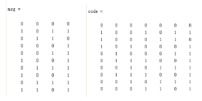
Figure 4.1 Matlab simulation diagram of Hamming code coding
10 random numbers are generated by using the random function of Matlab, and the 10 random functions are coded by 74 Hamming code coding function. The noise is introduced after coding, as shown in Figure 4.2:
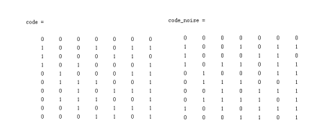
Figure 4.2 comparison between coding and adding noise
Decode through the decoding function, as shown in Figure 4.3 below:
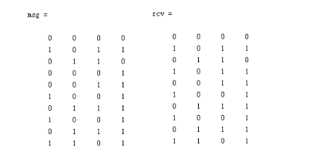
Figure 4.3 comparison between before coding and after decoding
According to figure 4.3, when one bit code value error occurs, Hamming decoding module can correct the error; When more than one bit code value error occurs, Hamming decoding module cannot correct the error, resulting in decoding error. Using Matlab, it can be seen that Hamming decoding module has decoding ability and error correction ability of one bit code value.
Use Verilog to write Hamming code coding module and Hamming decoding module, and then debug them together. Add a noise module in the middle of the two modules to ensure that any bit of the encoded data is wrong. After passing through the decoding module, judge whether the correct error correction can be carried out, whether the data before coding is consistent with the data after coding, and judge the correctness of the two modules, The debugging model is shown in Figure 4.4:
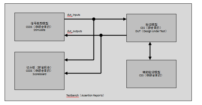
Figure 4.4 assertion debugging model
The screenshot of ModelSim simulation waveform is shown in Figure 4.5:

Figure 4.5 simulation waveform of Hamming codec module
The report is printed in the simulation mode of assertion, as shown in Figure 4.6. The correctness of Hamming coding module and Hamming decoding module is also proved by confirming the consistency of data before and after encoding and decoding.
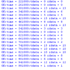
Figure 4.6 print result
4.2 direct sequence spread spectrum module commissioning
The module is debugged by Matlab, and the pseudo-random number is generated by Matlab pseudo-random function. By setting the initial value, it is compared with the results in table 3.2 in section 3.4.2. Through the comparison, it can be determined that the generated pseudo-random sequence meets the requirements, which lays a solid foundation for Verilog design. Figure 4.7 shows the pseudo-random number generated by Matlab, and the corresponding Matlab code is shown in Appendix A.

Figure 4.7 pseudo random number generated by MATLAB
4.3 synchronization module commissioning
During synchronous debugging, the synchronization head is not aligned. For example, the delay time for calculation should be 29 system clock cycles, that is, the counter only needs to delay 29 clock cycles, because the counter starts counting from "0". When the count value is equal to the delay time - 1, the module can de expand the synchronization head. Because the synchronization head is not aligned, As a result, the results calculated by the least square method are greater than the preset threshold, and the system cannot continue. The screenshot of simulation waveform is shown in Figure 4.8:

Figure 4.8 simulation waveform of synchronization error
According to the simulation waveform and the design code, the reason is finally found. Since the synchronization module also needs a system clock cycle to capture the delay time signal, the count value of the counter should be equal to the delay time - 2 before the module can carry out the synchronization head despreading. The screenshot of the simulation waveform is shown in Figure 4.9:

Figure 4.9 correct simulation waveform diagram of synchronous modification
4.4 overall design resource occupancy
After the design is completed, as shown in Figure 4.10, the overall design uses 3735 combinational logic, accounting for 5%; 1782 registers are used, accounting for 3%; Use 39 I/O pins, accounting for 6%; 5888 memories are used, accounting for about 1%; Two 9bit embedded hardware multipliers are used, accounting for about 1%.
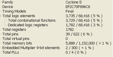
Figure 4.10 FPGA resource occupancy
4.5 overall design RTL view
It is inconsistent with the overall design block diagram due to instantiation, because instantiation has no impact on its overall design function. Therefore, the overall RTL view of the design is shown in Figure 4.11:
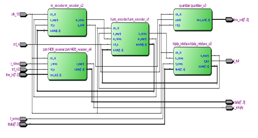
Figure 4.11 overall RTL diagram of design
5, System test
Test the overall system design, and test each module level by level from the sending end to the receiving end to ensure the correctness of each link.
5.1 Hamming coding module test
Use Verilog to write Hamming code coding module. In the testbench test file, the total input data is initialized to 8'h55 and reversed by the arrival of the rising edge of the clock, so the data are 8'h55, 8'haa, 8'h55... 8'haa in turn. The interface uses synchronous fifo for data buffering, as shown in Figure 5.1. In the test file, it passes judgment T_ The full signal is highly effective to judge whether fifo is in the full state. If it is not in the full state, set the enable signal t of the write operation_ Wrreq high level is valid, write to fifo, otherwise do not write. Hamming code coding module through judgment h_empty signal to determine whether fifo is empty. If it is not empty, set the read operation enable signal h_rdreq high level can effectively read fifo, otherwise it will not be read.

Figure 5.1 FIFO interface diagram
The Hamming code is used to encode the data through the Hamming code coding module, as shown in Figure 5.2, the signal ha_data is the corresponding coding result. The 4'h5 code is 7'h2d and the 4'ha code is 7'h52. As shown in Figure 5.2, the Hamming coding module can encode correctly.

Figure 5.2 simulation waveform of Hamming code coding module ModelSim
5.2 direct sequence spread spectrum module test
The pseudo-random number module is written with Verilog. The initial value is 5'b00001 and the generated sequence is as shown in Figure 5.3. Signal m_bit is a pseudo-random number. Before the coded data signal is spread spectrum, the data information shall be added to the frame header 14 'b11110, and the signal m_data refers to the 7bits data information encoded by hamming coding module, and the signal is s_bit is the signal after parallel serial conversion of frame header or encoded data information, and signal bc controls signal s_bit which data is in signal M_ If the bits are different or, the result is the output signal q_data, so as to realize the function of direct sequence spread spectrum. As shown in Figure 5.3, the direct sequence spread spectrum module can correctly complete the spread spectrum.


Figure 5.3 simulation waveform of direct sequence spread spectrum module ModelSim

5.3 quantizer module test
The quantizer module changes the single bit signal into 8 bits signed number. The screenshot of the simulation waveform is shown in Fig. 5.4. It can be determined that the quantizer module can quantize the signal correctly.

Figure 5.4 simulation waveform of quantizer module ModelSim

5.4 synchronization module test
In order to simulate the actual transmission process, the spread spectrum signal introduces ± 46 noise before entering the synchronization module. The actual input value signal line is shown in Figure 5.5:

Figure 5.5 ModelSim simulation waveform after adding noise
The least square method is used to calculate the input signal and 31 templates to obtain the only delay data signal xx less than the threshold. As shown in Figure 5.6, template 2 meets the requirements and the calculated value of signal xx is 29. Therefore, the delay of 29 beat despreading clock cycle is required to align the synchronization head.


Figure 5.6 simulation waveform of ModelSim for calculating delay
The purpose of aligning the synchronization head is achieved through delay, and the alignment enable signal en_m is high, indicating that it is aligned. As shown in Figure 5.7:

Figure 5.7 simulation waveform of synchronization head alignment ModelSim
After alignment, calculate the data signal with template "0" and template "1" by least square method every 31 bits, as shown in Figure 5.8:

Fig. 5.8 simulation waveform of synchronization head despreading ModelSim
Signal data_tm is the judged signal data. When the "0" data information of the last bit of the synchronization head is detected, it indicates that the synchronization head has ended and the synchronization function has been realized. As shown in Figure 5.9, the synchronization module can realize synchronization correctly.

Figure 5.9 simulation waveform of synchronization head identification ModelSim

5.5 direct sequence despreading module test
When it is detected that the last bit is "0", it enters the data signal despreading process, which is similar to the synchronous header despreading, except that the despread data is written to the corresponding position of the register by using the count value of the counter, and the serial parallel conversion function is carried out at the same time. The signal bc is the counter and the signal hdata_reg1 is a register that stores data after serial parallel conversion. As shown in Figure 5.10, the direct sequence despreading module can correctly realize despreading.


Figure 5.10 simulation waveform of data information despreading ModelSim
5.6 Hamming decoding module test
Use Verilog to write Hamming decoding module. The data after direct sequence despreading module passes through Hamming decoding module, as shown in Figure 5.11:

Figure 5.11 simulation waveform of Hamming decoding ModelSim
Signal data_ After reg is decoded correctly, it passes through the full flag signal h of fifo_ Full determines the high level. If it is high level, no write operation will be carried out. If it is low level, set the write enable signal of fifo high for write operation, and write the decoded data into fifo. As shown in Figure 5.12, Hamming decoding module can decode data correctly.
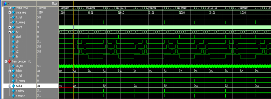
Figure 5.12 simulation screenshot of data output port
5.7 overall system test
Through the confirmation of printing information, the original data is consistent with the decoded data, and the overall design of the system can be confirmed to be correct, as shown in Figure 5.13:
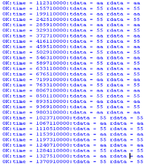
Figure 5.13 screenshot of print results
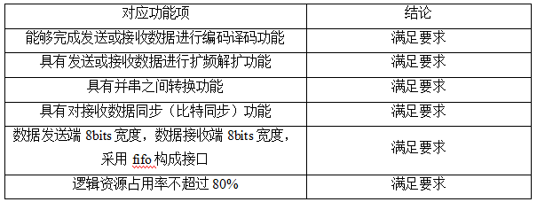
Referring to the design requirements in Section 2.1, summarize the corresponding functions completed in the overall design of the system, as shown in table 5.1:
Table 5.1 system function test table
Conclusion
Direct sequence spread spectrum is one of the mainstream spread spectrum communication, which has many important characteristics and advantages. This paper uses the processing speed and parallel operation of FPGA to design a spread spectrum module based on FPGA. The direct sequence spread spectrum module is simulated and analyzed by using Quartus II, Matlab and ModelSim. Using pseudo-random sequence to spread spectrum is the key to obtain high anti-noise performance and anti-interference performance of spread spectrum module.
This paper first introduces the general principle of direct sequence spread spectrum module, and then focuses on the analysis of direct sequence spread spectrum despreading, rational allocation of functional modules, accurate grasp of the control and controlled relationship between each module, as well as the overall timing relationship. After reading the data from the interface fifo, the Hamming coding module is used to complete the coding of the data. After the coding, the synchronization head is added to prepare for synchronization. The original polynomial is used to generate pseudo-random number, and the pseudo-random number is XOR processed with the encoded data to achieve the purpose of spread spectrum. The spread spectrum data is quantized and noise is introduced into the synchronization module. The synchronization module uses the template of 31 pseudo-random numbers and uses the least square method to calculate the data. If the calculated value is less than the predetermined threshold, the information corresponding to the data is the number of delayed beats required by the receiving end. After alignment, the template of 2 pseudo-random numbers is used to judge the "0" and "1" of the data. When the data value of the synchronization head appears "0", Represents that the next bit starts with data information, and the direct sequence despreading module starts despreading processing. Similarly to the synchronization module, the data and two pseudo-random are calculated by the least square method, so as to achieve the purpose of despreading. The despread data is decoded by hamming decoding module, written into interface fifo, and then output through fifo. After verification, the whole module achieves the purpose of spread spectrum, improves the anti noise ability, and each module can correctly complete the corresponding functions.
Appendix part of the source code
Pseudo random number Matlab code:
polynomial=[1 0 0 1 0 1];
reg=[0 0 0 0 1];
grade=length(polynomial)-1;
PN_Length=(2^grade-1);
pn=zeros(1,PN_Length);
n=0; c=zeros(1,grade);
for i=grade:-1:1
    if polynomial(i)==1
        n=n+1;
        c(n)=grade+1-i;
    end
end
q=0;
 for i=1:PN_Length
    p(i)=reg(1)
    m=reg(grade+1-c(1));
    for q=2:grade
        if (c(q)>0) & (reg(grade+1-c(q))==1)
            m=~m;
        end
    end
    for q=1:(grade-1)
        reg(q)=reg(q+1);
    end
    reg(5)=m;
end
Hamming code coding and decoding Matlab code:
k=4;
n=7;
msg=randint(10,4,2)
code=encode(msg,n,k)
code_noise=rem(code+rand(10,7)>0.95,2)
rcv=decode(code_noise,n,k)
disp(['Error rate in the received code:' num2str(symerr(code,code_noise)/length(code))])
disp(['Error rate after decode:' num2str(symerr(msg,rcv)/length(msg))])
Hamming code Verilog code:
module hamming74(clk_10, rst_n, hi_data, ha_data, hm_sel);
  input clk_10;
  input rst_n;
  input [7:0] hi_data;
  output reg [6:0] ha_data;
  input hm_sel;

  wire [3:0] hm_data;
  wire q0,q1,q2;

  assign hm_data = hm_sel ? hi_data[7:4] : hi_data[3:0];

  always @ (posedge clk_10)
  begin
    if(!rst_n)
      begin
        ha_data <= 0;
      end
    else
      begin
        ha_data[6] <= hm_data[3];
        ha_data[5] <= hm_data[2];
        ha_data[4] <= hm_data[1];
        ha_data[3] <= q2;
        ha_data[2] <= hm_data[0];
        ha_data[1] <= q1;
        ha_data[0] <= q0;
      end
  end

  assign  q0 = hm_data[0] ^ hm_data[1] ^ hm_data[3];
  assign  q1 = hm_data[0] ^ hm_data[2] ^ hm_data[3];
  assign  q2 = hm_data[1] ^ hm_data[2] ^ hm_data[3];
endmodule
Verilog code generated by pseudo-random number:
module m_generator(clk_10, rst_n, m_bit);

  input clk_10;
  input rst_n;
  output m_bit;

  reg [4:0] q;
  parameter KEY = 5'b00001;

  always @ (posedge clk_10)
  begin
    if(!rst_n)
      begin
        q <= KEY;
//        q <= 0;
      end
    else  begin
        q[0] <= q[1];
        q[1] <= q[2];
        q[2] <= q[3];
        q[3] <= q[4];
        q[4] <= q[3] ^ q[0];
      end
  end

  assign m_bit = q[0];

endmodule
Pseudo random sequence and data information XOR processing Verilog code:
module me_xor(clk, rst_n, s_bit, m_bit, q_data);

  input clk, rst_n;
  input s_bit, m_bit;
  output  reg q_data;

  always @ (posedge clk)
  begin
    if (!rst_n)
      q_data <= 0;
    else
      q_data <= s_bit ^ m_bit;
  end

endmodule
Verilog code of quantizer module:
module quantizer(clk, rst_n, qdata, line_out);

  input clk, rst_n;
  input qdata;
  output reg signed [7:0] line_out;

  always @ (posedge clk)
  begin
    if (!rst_n)
      line_out <= 0;
    else
      if (qdata)
        line_out <= 63;
      else
        line_out <= -64;
  end

endmodule
Least squares Verilog code:
module m_leastsquare(clk_10, rst_n, line, distance);
  input clk_10, rst_n;
  input signed [7:0] line;
  output reg signed [21:0] distance;
  parameter KEY = 5'b00001;
  wire m;
  reg [4:0] count;
  reg signed [21:0] int_distance;

  always @ (posedge clk_10)
  begin
    if (!rst_n || count >= 5'd30)
      count <= 0;
    else
      count <= count + 5'd1;
  end
  m_generator #(.KEY(KEY)) u_mg(.clk_10(clk_10), .rst_n(rst_n), .m_bit(m));
  always @ (posedge clk_10)
  begin
    if (!rst_n)
      begin
        int_distance <= 0;
        distance <= 0;
      end
    else
      if (count < 5'd30)
        if (!m)
          int_distance <= int_distance + (line - 63) * (line - 63);
        else
          int_distance <= int_distance + (line + 64) * (line + 64);
      else
        begin
          int_distance <= 0;
          if (!m)
            distance <= int_distance +  (line - 63) * (line - 63);
          else
            distance <= int_distance +  (line + 64) * (line + 64);
        end
  end
endmodule
Code of Verilog part of synchronization module:
module test_mdecoder_ls(clk_10, rst_n, line, xx);
  input clk_10, rst_n;
  input signed [7:0] line;
  output reg [5:0] xx;
  wire signed [21:0] distance [30:0];
  wire [30:0] xx_reg;
  integer i;
m_leastsquare #(.KEY(5'h01)) u0(.clk_10(clk_10), .rst_n(rst_n), .line(line), .distance(distance[0]));
  m_leastsquare #(.KEY(5'h10)) u1(.clk_10(clk_10), .rst_n(rst_n), .line(line), .distance(distance[1]));
  m_leastsquare #(.KEY(5'h08)) u2(.clk_10(clk_10), .rst_n(rst_n), .line(line), .distance(distance[2]));
  m_leastsquare #(.KEY(5'h14)) u3(.clk_10(clk_10), .rst_n(rst_n), .line(line), .distance(distance[3]));
  m_leastsquare #(.KEY(5'h0A)) u4(.clk_10(clk_10), .rst_n(rst_n), .line(line), .distance(distance[4]));
  m_leastsquare #(.KEY(5'h15)) u5(.clk_10(clk_10), .rst_n(rst_n), .line(line), .distance(distance[5]));
  m_leastsquare #(.KEY(5'h1A)) u6(.clk_10(clk_10), .rst_n(rst_n), .line(line), .distance(distance[6]));
  m_leastsquare #(.KEY(5'h1D)) u7(.clk_10(clk_10), .rst_n(rst_n), .line(line), .distance(distance[7]));
  m_leastsquare #(.KEY(5'h0E)) u8(.clk_10(clk_10), .rst_n(rst_n), .line(line), .distance(distance[8]));
  m_leastsquare #(.KEY(5'h17)) u9(.clk_10(clk_10), .rst_n(rst_n), .line(line), .distance(distance[9]));
  m_leastsquare #(.KEY(5'h1B)) u10(.clk_10(clk_10), .rst_n(rst_n), .line(line), .distance(distance[10]));
  m_leastsquare #(.KEY(5'h0D)) u11(.clk_10(clk_10), .rst_n(rst_n), .line(line), .distance(distance[11]));
  m_leastsquare #(.KEY(5'h06)) u12(.clk_10(clk_10), .rst_n(rst_n), .line(line), .distance(distance[12]));
  m_leastsquare #(.KEY(5'h03)) u13(.clk_10(clk_10), .rst_n(rst_n), .line(line), .distance(distance[13]));
  m_leastsquare #(.KEY(5'h11)) u14(.clk_10(clk_10), .rst_n(rst_n), .line(line), .distance(distance[14]));
  m_leastsquare #(.KEY(5'h18)) u15(.clk_10(clk_10), .rst_n(rst_n), .line(line), .distance(distance[15]));
  m_leastsquare #(.KEY(5'h1C)) u16(.clk_10(clk_10), .rst_n(rst_n), .line(line), .distance(distance[16]));
  m_leastsquare #(.KEY(5'h1E)) u17(.clk_10(clk_10), .rst_n(rst_n), .line(line), .distance(distance[17]));
  m_leastsquare #(.KEY(5'h1F)) u18(.clk_10(clk_10), .rst_n(rst_n), .line(line), .distance(distance[18]));
  m_leastsquare #(.KEY(5'h0F)) u19(.clk_10(clk_10), .rst_n(rst_n), .line(line), .distance(distance[19]));
  m_leastsquare #(.KEY(5'h07)) u20(.clk_10(clk_10), .rst_n(rst_n), .line(line), .distance(distance[20]));
  m_leastsquare #(.KEY(5'h13)) u21(.clk_10(clk_10), .rst_n(rst_n), .line(line), .distance(distance[21]));
  m_leastsquare #(.KEY(5'h19)) u22(.clk_10(clk_10), .rst_n(rst_n), .line(line), .distance(distance[22]));
  m_leastsquare #(.KEY(5'h0C)) u23(.clk_10(clk_10), .rst_n(rst_n), .line(line), .distance(distance[23]));
  m_leastsquare #(.KEY(5'h16)) u24(.clk_10(clk_10), .rst_n(rst_n), .line(line), .distance(distance[24]));
  m_leastsquare #(.KEY(5'h0B)) u25(.clk_10(clk_10), .rst_n(rst_n), .line(line), .distance(distance[25]));
  m_leastsquare #(.KEY(5'h05)) u26(.clk_10(clk_10), .rst_n(rst_n), .line(line), .distance(distance[26]));
  m_leastsquare #(.KEY(5'h12)) u27(.clk_10(clk_10), .rst_n(rst_n), .line(line), .distance(distance[27]));
  m_leastsquare #(.KEY(5'h09)) u28(.clk_10(clk_10), .rst_n(rst_n), .line(line), .distance(distance[28]));
  m_leastsquare #(.KEY(5'h04)) u29(.clk_10(clk_10), .rst_n(rst_n), .line(line), .distance(distance[29]));
  m_leastsquare #(.KEY(5'h02)) u30(.clk_10(clk_10), .rst_n(rst_n), .line(line), .distance(distance[30]));
  assign xx_reg[0] = (distance[0]>0 && distance[0]< 19'd50000)? 1'b1:1'b0;
  assign xx_reg[1] = (distance[1]>0 && distance[1]< 19'd50000)? 1'b1:1'b0;
  assign xx_reg[2] = (distance[2]>0 && distance[2]< 19'd50000)? 1'b1:1'b0;
  assign xx_reg[3] = (distance[3]>0 && distance[3]< 19'd50000)? 1'b1:1'b0;
  assign xx_reg[4] = (distance[4]>0 && distance[4]< 19'd50000)? 1'b1:1'b0;
  assign xx_reg[5] = (distance[5]>0 && distance[5]< 19'd50000)? 1'b1:1'b0;
  assign xx_reg[6] = (distance[6]>0 && distance[6]< 19'd50000)? 1'b1:1'b0;
  assign xx_reg[7] = (distance[7]>0 && distance[7]< 19'd50000)? 1'b1:1'b0;
  assign xx_reg[8] = (distance[8]>0 && distance[8]< 19'd50000)? 1'b1:1'b0;
  assign xx_reg[9] = (distance[9]>0 && distance[9]< 19'd50000)? 1'b1:1'b0;
  assign xx_reg[10] = (distance[10]>0 && distance[10]< 19'd50000)? 1'b1:1'b0;
  assign xx_reg[11] = (distance[11]>0 && distance[11]< 19'd50000)? 1'b1:1'b0;
  assign xx_reg[12] = (distance[12]>0 && distance[12]< 19'd50000)? 1'b1:1'b0;
  assign xx_reg[13] = (distance[13]>0 && distance[13]< 19'd50000)? 1'b1:1'b0;
  assign xx_reg[14] = (distance[14]>0 && distance[14]< 19'd50000)? 1'b1:1'b0;
  assign xx_reg[15] = (distance[15]>0 && distance[15]< 19'd50000)? 1'b1:1'b0;
  assign xx_reg[16] = (distance[16]>0 && distance[16]< 19'd50000)? 1'b1:1'b0;
  assign xx_reg[17] = (distance[17]>0 && distance[17]< 19'd50000)? 1'b1:1'b0;
  assign xx_reg[18] = (distance[18]>0 && distance[18]< 19'd50000)? 1'b1:1'b0;
  assign xx_reg[19] = (distance[19]>0 && distance[19]< 19'd50000)? 1'b1:1'b0;
  assign xx_reg[20] = (distance[20]>0 && distance[20]< 19'd50000)? 1'b1:1'b0;
  assign xx_reg[21] = (distance[21]>0 && distance[21]< 19'd50000)? 1'b1:1'b0;
  assign xx_reg[22] = (distance[22]>0 && distance[22]< 19'd50000)? 1'b1:1'b0;
  assign xx_reg[23] = (distance[23]>0 && distance[23]< 19'd50000)? 1'b1:1'b0;
  assign xx_reg[24] = (distance[24]>0 && distance[24]< 19'd50000)? 1'b1:1'b0;
  assign xx_reg[25] = (distance[25]>0 && distance[25]< 19'd50000)? 1'b1:1'b0;
  assign xx_reg[26] = (distance[26]>0 && distance[26]< 19'd50000)? 1'b1:1'b0;
  assign xx_reg[27] = (distance[27]>0 && distance[27]< 19'd50000)? 1'b1:1'b0;
  assign xx_reg[28] = (distance[28]>0 && distance[28]< 19'd50000)? 1'b1:1'b0;
  assign xx_reg[29] = (distance[29]>0 && distance[29]< 19'd50000)? 1'b1:1'b0;
  assign xx_reg[30] = (distance[30]>0 && distance[30]< 19'd50000)? 1'b1:1'b0;
  always @ (*)
  begin
    if(!rst_n)
      begin
        xx <= 6'd32;
      end
    else
      begin
        for(i=0;i<30;i=i+1)
          if(xx_reg[i]==1)
            xx <= 31-i;
      end
  end
endmodule
Verilog code of direct sequence despreading module:
module test_mdecoder_2s(clk_10, rst_n, line, data_tm, en_m); //Test, least square method

  input clk_10, rst_n;
  input signed [7:0] line;
  output data_tm;
  input en_m;
  wire signed [30:0] distance [1:0];
  wire [30:0] reg1 , reg0 ;

  m_leastsquare_nl #(.KEY(5'h01)) u32(.clk_10(clk_10), .rst_n(rst_n), .line(line), .distance(distance[0]), .en_m(en_m));//0
  m_leastsquare_no #(.KEY(5'h01)) u33(.clk_10(clk_10), .rst_n(rst_n), .line(line), .distance(distance[1]), .en_m(en_m));//1

  assign data_tm = ( distance[1]>distance[0])? 1'b0:1'b1;//Compare two data sizes

endmodule
Hamming decoding Verilog code:
module deserialzer(clk_10, rst_n, data_tm, en_m, hdata, h_full, h_wrreq);
/*    Serial to parallel module plus Hamming decoding module    */
  input clk_10;
  input rst_n;
  input data_tm;
  input en_m;
  output reg [7:0] hdata;
  input h_full;
  output reg h_wrreq;
  reg [5:0] count;
  reg [2:0] bc;
  reg [6:0] hdata_reg1;
  reg start;
  wire c0,c1,c2;
  reg lh;
  reg [3:0] data_reg;
  /*  Used to calculate data bits  */
  always @ (posedge clk_10)
  begin
    if(!rst_n)
      begin
        count <= 0;
        bc <= 0;
      end
    else if(en_m && count < 30)
      count <= count + 6'd1;
    else
      begin
        if(count == 6'd30 && bc < 3'd6)
          bc <= bc + 3'd1;
        else
          bc <= 0;
      count <= 0;
      end
  end
  /*  Used to buffer data  */
  always @ (posedge clk_10)
  begin
    hdata_reg1[bc] <= data_tm;
  end
  /*  It is used to control the data to be written in high and low order, and control the sending and writing enable at the same time  */
  always @ (posedge clk_10)
  begin
    if(!rst_n)
      begin
        h_wrreq <= 0;
        lh <= 1;
      end
    else if(!h_full && bc == 3'd6 && count == 6'd30)
        begin
          lh <= ~lh;
          if(lh)
            h_wrreq <= 0;
          else
            h_wrreq <= 1;
        end
    else
      h_wrreq <= 0;
  end
  /*  Enable used to control decoding  */
  always @ (posedge clk_10)
  begin
    if(!rst_n)
      begin
        start <= 0;

      end
    else if(!h_full && bc == 3'd6 && count == 6'd29)
        begin
          start <= 1;
        end
    else
      start <= 0;
  end
  assign c0 = hdata_reg1[0] ^ hdata_reg1[2] ^ hdata_reg1[4] ^ hdata_reg1[6];
  assign c1 = hdata_reg1[1] ^ hdata_reg1[2] ^ hdata_reg1[5] ^ hdata_reg1[6];
  assign c2 = hdata_reg1[3] ^ hdata_reg1[4] ^ hdata_reg1[5] ^ hdata_reg1[6];
  /*  Used for high and low data assignment  */
  always @ (*)
  begin
    if(lh)
      hdata[7:4] <= data_reg;
    else
      hdata[3:0] <= data_reg;
  end
  always @ (posedge clk_10)
  begin
    if(!rst_n)
      begin
        data_reg <= 0;
      end
    else if (start)
        case({c2,c1,c0})
      3'b000:begin//No mistake
        data_reg[3] <= hdata_reg1[6];
        data_reg[2] <= hdata_reg1[5];
        data_reg[1] <= hdata_reg1[4];
        data_reg[0] <= hdata_reg1[2];
      end
      3'b001:begin//Check bit HC_ Error in [0]
        data_reg[3] <= hdata_reg1[6];
        data_reg[2] <= hdata_reg1[5];
        data_reg[1] <= hdata_reg1[4];
        data_reg[0] <= hdata_reg1[2];
      end
      3'b010:begin//Check bit HC_ Error in [1]
        data_reg[3] <= hdata_reg1[6];
        data_reg[2] <= hdata_reg1[5];
        data_reg[1] <= hdata_reg1[4];
        data_reg[0] <= hdata_reg1[2];
      end
      3'b011:begin//Check bit hc_in[0],hc_ Error in [1]
        data_reg[3] <= hdata_reg1[6];
        data_reg[2] <= hdata_reg1[5];
        data_reg[1] <= hdata_reg1[4];
        data_reg[0] <= ~hdata_reg1[2];
      end
      3'b100:begin//Check bit HC_ Error in [2]
        data_reg[3] <= hdata_reg1[6];
        data_reg[2] <= hdata_reg1[5];
        data_reg[1] <= hdata_reg1[4];
        data_reg[0] <= hdata_reg1[2];
      end
      3'b101:begin//Check bit hc_in[0],hc_ Error in [2]
        data_reg[3] <= hdata_reg1[6];
        data_reg[2] <= hdata_reg1[5];
        data_reg[1] <= ~hdata_reg1[4];
        data_reg[0] <= hdata_reg1[2];
      end
      3'b110:begin//Check bit hc_in[1],hc_ Error in [2]
        data_reg[3] <= hdata_reg1[6];
        data_reg[2] <= ~hdata_reg1[5];
        data_reg[1] <= hdata_reg1[4];
        data_reg[0] <= hdata_reg1[2];
      end
      3'b111:begin//Check bit hc_in[1],hc_in[2],hc_ Error in [0]
        data_reg[3] <= ~hdata_reg1[6];
        data_reg[2] <= hdata_reg1[5];
        data_reg[1] <= hdata_reg1[4];
        data_reg[0] <= hdata_reg1[2];
      end
    endcase
  end

endmoduleThe follow-up will be continuously updated, bringing installation related design tutorials such as Vivado, ISE, Quartus II and candence, learning resources, project resources, good article recommendations, etc. I hope you will continue to pay attention.
Heroes, the Jianghu is so big. Continue to wander. May everything be well. See you again!