Hello, great Xia. Welcome to the FPGA technology Jianghu. The Jianghu is so big. It's fate to meet each other.
The design of USB interface based on FPGA brings three chapters to today. Today, I will bring the third and second parts, FPGA firmware development, USB driver and software development. Don't talk much, load the goods.
Hyperlinks to the first two articles are also given here:
Design of USB interface controller based on FPGA (VHDL) (Part I)
Design of USB interface controller based on FPGA (VHDL) (medium)
Previously, there was a USB interface controller design implemented by Verilog HDL. Here are hyperlinks for your reference only.
Source code series: USB2 based on FPGA 0 design
Reading guide
On September 4, 2019, USB-IF finally officially announced the USB 4 specification. It introduces the Thunderbolt lightning protocol specification previously donated by Intel to the USB promotion organization. The two lane operation improves the transmission bandwidth, which is the same as that of lightning 3, both of which are 40Gbps. It should be noted that if you want to experience the highest transmission speed, you must use a new certified data cable. USB4 retains good compatibility and can be downward compatible with USB 3.2/3.1/3.0 and lightning 3. In addition, USB4 will only have one USB Type-C interface and support a variety of data and display protocols, including DisplayPort, which can make full use of high-speed bandwidth and support USB PD power supply.
Unfortunately, the release time of USB4 has not been announced yet. It is worth noting that USB4 released this time is a specification, not USB4 0 Before that, USB Implementers Forum (USB-IF) plans to cancel the naming of USB 3.0/3.1 and uniformly classify it as USB 3.2. Among them, USB 3.0 was renamed USB 3.2 Gen 1 (5Gbps), USB 3.1 was renamed USB 3.2 Gen 2(10Gbps), and USB 3.2 was renamed USB 3.2 Gen 2x2 (20Gbps). The above is the information about USB standard and naming.
Now most USB devices (such as USB interface mouse, keyboard, flash memory, USB flash disk, etc.) use USB universal drive, and if your system has USB universal drive (such as XP has built-in USB universal drive), you can use it. Some USB devices need special drivers. For example, some mobile phones need to install drivers to connect to the USB port of the computer. Now let's do the design of USB interface controller and learn how to design it.
Abstract of the third part: this part will introduce the development of FPGA firmware, including the division of firmware module, the compilation of user-defined package, the realization of frequency divider module, the realization of edge control module, the realization of input / output switching module, the realization of request processing module, the realization of equipment transceiver module and the compilation of test platform; USB driver and software development, including USB driver writing, USB software writing and summary.
6, FPGA firmware development6.1 firmware module division
In this example, firmware development refers to FPGA development, that is, using hardware description language (VHDL or Verilog HDL) to write FPGA internal program. The function of FPGA is to communicate with PDIUSBD12, obtain data from PDIUSBD12 and send data according to the requirements of the host. The communication between PDIUSBD12 and FPGA is an 8-bit data bus plus several control signals (A0, WR_N, RD_N, etc.). The communication between them can be realized as long as the FPGA is controlled to generate pulses conforming to the input / output timing of PDIUSBD12.
The module diagram of FPGA firmware is shown in Figure 34, and the functions of each module are as follows.
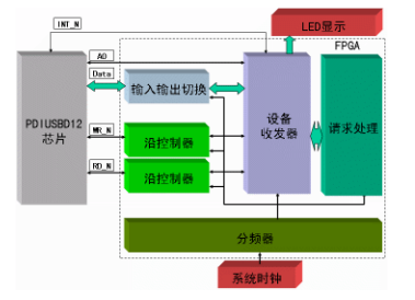
Figure 34 design scheme of hardware encryption system
(1) Frequency divider module
Because PDIUSBD12 has time limit on reading and writing timing, for example, the interval between each reading and writing operation cannot be less than 500ns, and the system clock frequency of FPGA is generally high, so the system clock cannot be directly used to control PDIUSBD12, and frequency division must be carried out. The function of the frequency divider module is to generate the clock signal of the required frequency from the system clock according to the requirements.
(2) Along the controller module
The read and write operations of PDIUSBD12 each have a read and write control signal WR_N and RD_N. Each read-write operation is triggered at the falling edge of the corresponding control signal. The function of the edge control module is to controllably generate a falling edge signal for controlling the read-write operation.
(3) Input / output switching module
The input / output switching module is very important in the whole system, because the data bus between FPGA chip and PDIUSBD12 chip is a bidirectional bus, so when one of the read-write operations is in progress, the signal source of the other operation must be turned off, otherwise it will cause double drive, which will not only not get correct data, but also damage the chip. The function of the input / output switching module is to control the signal source according to the current reading and writing status to ensure that only one signal source is driving the bus at a time.
(4) Device transceiver module
This module is the core module of the whole firmware. Its work includes configuring the PDIUSBD12 chip, processing the interrupt generated by PDIUSBD12, reading data from the cache, and sending the data through PDIUSBD12 as needed. The device transceiver module completes the parsing of each host request. In addition, it also transmits the parsed request data to the request processing module.
(5) Request processing module
The function of the request processing module is to receive the host request parsed by the device transceiver module and decide how to process the request.
After the module division, you can use ISE to create the project, then write the implementation code and test platform for each module, and finally integrate all modules as an entity, simulate and test them, which is a complete FPGA development process.
Some basic use methods of ISE have been introduced in detail in the previous article. Hyperlinks are placed here and will not be described in detail here. The implementation methods of each module are introduced in detail below.
ISE 14.7 installation tutorial and detailed instructions
6.2 user defined package writing
Before actually realizing the functions of each module, you need to write two user-defined packages, namely USB package and PDIUSBD12 package.
USB package defines the USB protocol and data types and constants related to USB devices, such as user-defined data types, device type code values, request code values, device descriptors, working state machines of devices, etc. The working state machine of the equipment is defined as follows:
- Define the working state machine of the device
type TRANSEIVER_STATE
is ( TS_DISCONNECTED, -- Not connected
TS_CONNECTING, -- on connection
TS_IDLE, -- let ... lie idle
TS_END_REQUESTHANDLER, -- Request processing completed
TS_READ_IR, -- Read interrupt register
TS_READ_LTS, -- Read last processing status
TS_BUSRESET, -- Bus reset
TS_SUSPENDCHANGE, -- Pending changes
TS_EP0_RECEIVE, -- Endpoint 0 receive complete
TS_EP0_TRANSMIT, -- Endpoint 0 send complete
TS_EP2_RECEIVE, -- Endpoint 2 receive complete
TS_EP2_TRANSMIT, -- Endpoint 2 sending completed
TS_END_RECEIVE, -- from PDIUSBD12 Read data complete
TS_END_TRANSMIT, -- towards PDIUSBD12 Write data complete
TS_SEND_DESCRIPTOR_1ST, -- First send device descriptor
TS_SEND_DESCRIPTOR, -- Send device descriptor
TS_SET_ADDRESS, -- Set address
TS_SET_CONFIGURATION, -- set configuration
TS_GET_CONFIGURATION, -- Get configuration
TS_GET_INTERFACE, -- Get interface
TS_SEND_STATUS, -- Send status
TS_CLEAR_FEATURE, -- Clear properties
TS_SET_FEATURE, -- Enable properties
TS_SET_INTERFACE, -- Set interface
TS_READ_ENDPOINT, -- Read data from endpoint
TS_WRITE_ENDPOINT, -- Write data to endpoint
TS_SEND_PASSWORD, -- Send password
TS_SET_PASSWORD_HIGH, -- Set password low
TS_SET_PASSWORD_LOW, -- Set password high
TS_SEND_EMPTY_PACKET, -- Send empty packet
TS_STALL, -- prohibit
TS_ERROR); -- error
The request type and code are defined as follows:
-- Descriptor type
constant TYPE_DEVICE_DESCRIPTOR: STD_LOGIC_VECTOR(7 downto 0) := X"01";
constant TYPE_CONFIGURATION_DESCRIPTOR: STD_LOGIC_VECTOR(7 downto 0) := X"02";
constant TYPE_STRING_DESCRIPTOR: STD_LOGIC_VECTOR(7 downto 0) := X"03";
constant TYPE_INTERFACE_DESCRIPTOR: STD_LOGIC_VECTOR(7 downto 0) := X"04";
constant TYPE_ENDPOINT_DESCRIPTOR: STD_LOGIC_VECTOR(7 downto 0) := X"05";
constant TYPE_POWER_DESCRIPTOR: STD_LOGIC_VECTOR(7 downto 0) := X"06";

-- Code, index value, etc. related to device descriptor
constant CODE_DEVICE_CLASS: STD_LOGIC_VECTOR(7 downto 0) := X"DC";
constant CODE_BCD_USB_HIGH: STD_LOGIC_VECTOR(7 downto 0) := X"00";
constant CODE_BCD_USB_LOW: STD_LOGIC_VECTOR(7 downto 0) := X"01";
constant CODE_ID_VENDOR_HIGH: STD_LOGIC_VECTOR(7 downto 0) := X"71";
constant CODE_ID_VENDOR_LOW: STD_LOGIC_VECTOR(7 downto 0) := X"04";
constant CODE_ID_PRODUCT_HIGH: STD_LOGIC_VECTOR(7 downto 0) := X"66";
constant CODE_ID_PRODUCT_LOW: STD_LOGIC_VECTOR(7 downto 0) := X"06";
constant CODE_BCD_DEVICE_HIGH: STD_LOGIC_VECTOR(7 downto 0) := X"00";
constant CODE_BCD_DEVICE_LOW: STD_LOGIC_VECTOR(7 downto 0) := X"01";
constant CODE_NUMBER_CONFIGURATIONS: STD_LOGIC_VECTOR(7 downto 0) := X"19";
The other package is PDIUSBD12 package, which defines the contents related to PDIUSBD12, such as the command code value, interrupt code value and other contents of PDIUSBD12. The definition of PDIUSBD12 control command is as follows:
-- PDIUSBD12 control command
constant D12_COMMAND_ENABLE_ADDRESS: STD_LOGIC_VECTOR(7 downto 0) := X"D0";
constant D12_COMMAND_ENABLE_ENDPOINT: STD_LOGIC_VECTOR(7 downto 0) := X"D8";
constant D12_COMMAND_SET_MODE: STD_LOGIC_VECTOR(7 downto 0) := X"F3";
constant D12_COMMAND_SET_DMA: STD_LOGIC_VECTOR(7 downto 0) := X"FB";
constant D12_COMMAND_READ_IR: STD_LOGIC_VECTOR(7 downto 0) := X"F4";
constant D12_COMMAND_SEL_EP0_OUT: STD_LOGIC_VECTOR(7 downto 0) := X"00";
constant D12_COMMAND_SEL_EP0_IN: STD_LOGIC_VECTOR(7 downto 0) := X"01";
constant D12_COMMAND_SEL_EP1_OUT: STD_LOGIC_VECTOR(7 downto 0) := X"02";
constant D12_COMMAND_SEL_EP1_IN: STD_LOGIC_VECTOR(7 downto 0) := X"03";
constant D12_COMMAND_SEL_EP2_OUT: STD_LOGIC_VECTOR(7 downto 0) := X"04";
constant D12_COMMAND_SEL_EP2_IN: STD_LOGIC_VECTOR(7 downto 0) := X"05";
constant D12_COMMAND_READ_LTS_EP0_OUT: STD_LOGIC_VECTOR(7 downto 0) := X"40";
constant D12_COMMAND_READ_LTS_EP0_IN: STD_LOGIC_VECTOR(7 downto 0) := X"41";
constant D12_COMMAND_READ_LTS_EP1_OUT: STD_LOGIC_VECTOR(7 downto 0) := X"42";
constant D12_COMMAND_READ_LTS_EP1_IN: STD_LOGIC_VECTOR(7 downto 0) := X"43";
constant D12_COMMAND_READ_LTS_EP2_OUT: STD_LOGIC_VECTOR(7 downto 0) := X"44";
constant D12_COMMAND_READ_LTS_EP2_IN: STD_LOGIC_VECTOR(7 downto 0) := X"45";
constant D12_COMMAND_RW_BUFFER: STD_LOGIC_VECTOR(7 downto 0) := X"F0";
constant D12_COMMAND_ACK_SETUP: STD_LOGIC_VECTOR(7 downto 0) := X"F1";
constant D12_COMMAND_CLEAR_EP_BUFFER: STD_LOGIC_VECTOR(7 downto 0) := X"F2";
constant D12_COMMAND_ENABLE_BUFFER: STD_LOGIC_VECTOR(7 downto 0) := X"FA";
In view of space and other reasons, the above only introduces some contents of USB package and PDIUSBD12 package for reference.
6.3 implementation of frequency divider module
The basic principle of the frequency divider module is to design a counter working under the system clock, reduce or increase the count repeatedly, and flip the output at a fixed value of the count to realize the function of clock frequency division.
For example, the system clock on the experimental board is 50MHz, and the required reading and writing cycle interval is required to be greater than 500ns, that is, the reading and writing clock frequency cannot be higher than 2MHz, and the original system clock needs to be divided by at least 25 times. Therefore, we set a counter to work under the system clock. The count of each system clock cycle is reduced by one and then restored to 13 after it is reduced to zero. In this way, after 13 × 2 = 26 system clock cycles, and the output of the counter will be a complete cycle.
The schematic diagram of the frequency divider module is shown in Figure 35.
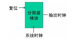
Figure 35 schematic diagram of frequency divider module
The code to realize the frequency divider module is as follows:
-- Declare the package used
library IEEE;
use IEEE.STD_LOGIC_1164.all;
use WORK.USB_PACKAGE.all;
-- Declarative entity
entity FrequencyDivider is
      generic(
              div_factor : INTEGER8 := 0 -- Frequency division coefficient attribute
        );
      port(
              reset_n : in STD_LOGIC; -- Reset port
              clk_origin : in STD_LOGIC; -- Input clock port
              clk : out STD_LOGIC -- Output clock port
        );
end FrequencyDivider;
architecture FrequencyDivider of FrequencyDivider is
-- Internal signal,It is changed internally at any time and output to the output clock port at the same time
signal clk_tmp: STD_LOGIC;
begin
    -- Signal connection
    clk <= clk_tmp;
    -- Main process
    main_process: process( reset_n, clk_origin )
    variable count: INTEGER8;
    begin
        if reset_n = '0' then
            count := 0;
            clk_tmp <= '0';
        elsif rising_edge(clk_origin) then
        -- Flip the output when the count reaches the frequency division coefficient,And reset the count
            if count = div_factor then
                clk_tmp <= not clk_tmp;
                count := 0;
            else
                count := count+1;
            end if;
        end if;
    end process;
end FrequencyDivider;
6.4 implementation of edge control module
The function of edge control module is to provide controllable falling edge output. The implementation scheme is as follows: use an enable signal CE_N control output. The input is the clock after frequency division, when CE_ When the N input is high, the output remains high, while when CE_ When the N input becomes low, connect the clock to the output, so as to obtain a continuous falling edge signal (synchronized with the falling edge of the clock). As long as the CE_ If n is properly controlled, the required falling edge can be obtained.
The schematic diagram and timing diagram along the control module are shown in Figure 36. The input clock is connected to the output clock of the frequency divider module, and the enable signal controls the edge output signal. As long as the enable signal is kept low in a certain clock cycle, a falling edge output can be obtained.
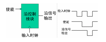
Fig. 36 schematic diagram and timing diagram along the control module
The implementation code of the control module is as follows:
--Declare the package used
library IEEE;
use IEEE.STD_LOGIC_1164.all;
-- Declarative entity
entity EdgeController is
    port(
          clk : in STD_LOGIC; -- Input clock port
          ce_n : in STD_LOGIC; -- Enable port
          edge : out STD_LOGIC -- Edge signal output port
      );
end EdgeController;
architecture EdgeController of EdgeController is
begin
    -- Output signal assignment
        edge <= clk when ce_n = '0' else
                '1';
end EdgeController;
6.5 implementation of I / O switching module
Since the 8-bit data line of PDIUSBD12 is a bidirectional bus, attention should be paid to avoid double driving when reading and writing. Double drive means adding output signals to the bus on both sides of the bus at the same time, so that the bus data is in an unstable state (represented by X) and it is easy to damage the device. For example, if the simulation waveform of dual drive is not handled properly, it will be as shown in Figure 37. In this case, correct data cannot be obtained.
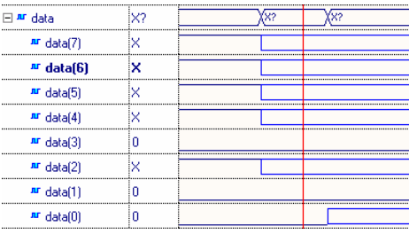
Fig. 37 simulation unsteady state sequence diagram
The four basic states of the signal are high level (1), low level (0), unstable state (X) and high resistance state (Z). When two signals are added to a bus at the same time, the combined results are shown in table 35.
Table 35 signal status
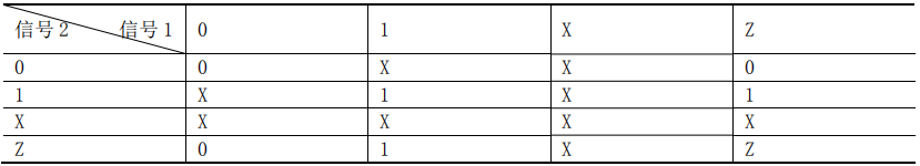
It can be seen that when there are two drives on a bus at the same time, it is likely to produce unstable state X, but if one signal is high resistance state Z, it is a determined state (i.e. the state of the other signal). Therefore, the basic idea of avoiding double drive is to turn off one drive source according to the current read-write state, that is, set the output of the other drive source to the high resistance state. Since the read-write operation is controlled by their respective control signals (WR_N, RD_N), the two signals can be used as mutually exclusive signals to control the signal source of bus data. For example, when Rd_ When n is low, if you want to read data from PDIUSBD12, you should turn off the output of FPGA to the bus, that is, the bus output signal of FPGA changes to high resistance state Z. The reverse is also true when wr_ When n is low, it is necessary to send data to PDIUSBD12. At this time, PDIUSBD12 will automatically turn off its output on the bus. The above ideas can be expressed as follows:

The schematic diagram of I / O switching module is shown in figure 6-38. The bus on the left represents the bus connected to PDIUSBD12, and the input and output buses on the right represent the bus signals inside the FPGA, indicating that the input and output of the bus are distinguished inside the FPGA; RD_N and wr_ The N signal is used for read and write control respectively.
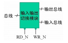
Figure 38 schematic diagram of input / output switching module
The implementation code of I / O switching module is as follows:
--Declare the package used
library IEEE;
use IEEE.STD_LOGIC_1164.all;
-- Declarative entity
entity IOSwitch is
    port(
          data : inout STD_LOGIC_VECTOR(7 downto 0); -- 8 Bit bidirectional data bus,and PDIUSBD12 to be connected
          din : in STD_LOGIC_VECTOR(7 downto 0); -- 8 Bit input data bus,For input only
          dout : out STD_LOGIC_VECTOR(7 downto 0); -- 8 Bit output data bus,For output only
          sel_in_n : in STD_LOGIC; -- Bus input control signal
          sel_out_n : in STD_LOGIC -- Bus output control signal
      );
end IOSwitch;

architecture IOSwitch of IOSwitch is
-- Create an internal signal,For data transfer
signal data_tmp : STD_LOGIC_VECTOR(7 downto 0);

begin
    -- Signal connection
    data <= data_tmp;
    dout <= data;
    -- Main process
    process(sel_in_n, sel_out_n, data, din)
    begin
        -- When the output control signal is valid,take data_tmp Assignment high resistance
        if sel_out_n = '0' then
            data_tmp <= "ZZZZZZZZ";
        -- When the input control signal is valid,Assign the input signal to data_tmp
        elsif sel_in_n = '0' then
            data_tmp <= din;
        else
            data_tmp <= "ZZZZZZZZ";
        end if;
    end process;
end IOSwitch;
6.6 implementation of request processing module
The function of the request processing module is to control the processing state of the device transceiver module according to the request of the host. In this example, the actual function of the request processing module is to control the transceiver module of the device to send data according to the host request received at present, so the implementation of the request processing module is a simple state machine.
The schematic diagram of the request processing module is shown in Figure 39. The clock signal is provided by the output clock of the frequency divider; The request type input is an 8-bit port, which works together with the receiving event input. When the device transceiver receives a request, it will send the request code to the request type input port, and the low level of a clock cycle will be output at the receiving event input port, indicating a new request processing; The command output port and command interrupt port are used to control the operation status of the device transceiver module.
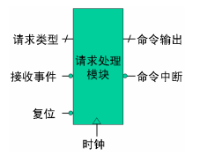
Fig. 39 schematic diagram of request processing module
The implementation code of the request processing module is as follows:
-- Declare the library to use
library IEEE;
use IEEE.STD_LOGIC_1164.all;
use WORK.USB_PACKAGE.all;
use WORK.PDIUSBD12_PACKAGE.all;
-- Declarative entity
entity RequestHandler is
    port(
            reset_n : in STD_LOGIC; -- Reset port
            clk : in STD_LOGIC; -- Input clock
            recv_n : in STD_LOGIC; -- Receive event input port
            req_type : in STD_LOGIC_VECTOR(7 downto 0); -- Request type input port
            cmd : out STD_LOGIC_VECTOR(7 downto 0); -- Command output port
            exec_n : out STD_LOGIC -- Command interrupt port
        );
end RequestHandler;

architecture RequestHandler of RequestHandler is
-- State machine,Already in USB Defined in package
signal rh_state: REQUEST_HANDLER_STATE := RH_IDLE;
-- register,Used to indicate whether an address has been assigned
signal address_set: STD_LOGIC := '0';
begin
    -- Main process
    main_process: process( reset_n, clk )
    begin
        if reset_n = '0' then
            -- reset output signals
            cmd <= X"00";
            exec_n <= '1';
            address_set <= '0';
            -- reset state machine
            rh_state <= RH_IDLE;
        elsif falling_edge(clk) then
            case rh_state is
            when RH_IDLE =>
                -- recv_n When it is low, it indicates that request processing is required
                if recv_n = '0' then
                    -- req_type Is the requested code
                    case req_type is
                    -- Get descriptor request
                    when REQUEST_GET_DESCRIPTOR =>
                        if address_set = '0' then
                            cmd <= RH_SEND_DESCRIPTOR_1ST;
                        else
                            cmd <= RH_SEND_DESCRIPTOR;
                        end if;
                        exec_n <= '0';
                    -- Get status request
                    when REQUEST_GET_STATUS =>
                        cmd <= RH_SEND_STATUS;
                        exec_n <= '0';
                    -- Set address status
                    when REQUEST_SET_ADDRESS =>
                        address_set <= '1';
                        cmd <= RH_SET_ADDRESS;
                        exec_n <= '0';
                    -- Enable feature request
                    when REQUEST_SET_FEATURE =>
                        cmd <= RH_SET_FEATURE;
                        exec_n <= '0';
                    -- Clear feature request
                    when REQUEST_CLEAR_FEATURE =>
                        cmd <= RH_CLEAR_FEATURE;
                        exec_n <= '0';
                    -- Set configuration request and set descriptor request
                    when
                        REQUEST_SET_CONFIGURATION | REQUEST_SET_DESCRIPTOR =>
                        cmd <= RH_SET_CONFIGURATION;
                        exec_n <= '0';
                    -- Get configuration request
                    when REQUEST_GET_CONFIGURATION =>
                        cmd <= RH_SEND_CONFIGURATION;
                        exec_n <= '0';
                    -- Set interface request
                    when REQUEST_SET_INTERFACE =>
                        cmd <= RH_SET_INTERFACE;
                        exec_n <= '0';
                    -- Get password request
                    when REQUEST_GET_PASSWORD =>
                        cmd <= RH_SEND_PASSWORD;
                        exec_n <= '0';
                    -- Get password request
                    when REQUEST_SET_PASSWORD_HIGH =>
                        cmd <= RH_SET_PASSWORD_HIGH;
                        exec_n <= '0';
                    -- Get password request
                    when REQUEST_SET_PASSWORD_LOW =>
                        cmd <= RH_SET_PASSWORD_LOW;
                        exec_n <= '0';
                    when others =>
                        NULL;
                    end case;
                else
                    exec_n <= '1';
                    cmd <= RH_INVALID_COMMAND;
                end if;
            when others =>
                NULL;
            end case;
        end if;
    end process;
end RequestHandler;
6.7 implementation of equipment transceiver module
The device transceiver module is the core of the whole firmware system. The basic idea of implementation is to create a state machine, treat each processing operation as a state, and access and control its data according to the timing requirements of PDIUSBD12 in each state.
The schematic diagram of the device transceiver module is shown in Figure 40.
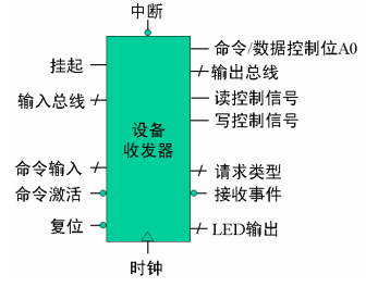
Figure 40 schematic diagram of device transceiver module
Because the USB protocol is very complex and the control of PDIUSBD12 is also complex, the state quantity of the device transceiver state machine will be more. According to the functions of the device transceiver, the functions of each state of the state machine can be divided into three categories.
• initialization device: initialization device is the state of configuring PDIUSBD12 device. The contents to be configured include setting address / enable, setting DMA and setting mode.
• data access: data access is to realize data reading and writing between PDIUSBD12 and FPGA, including reading interrupt register, reading previous transmission status, reading data by endpoint, sending data by endpoint, etc.
• request reply: request reply refers to extracting the required data according to the data format of various types of requests and notifying the request processing module after parsing. The implementation of the above three states is described in detail below.
1) Initialize device
The status related to the initialization device is mainly TS_DISCONNECTED and TS_CONNECTING (see USB_Package.vhd file for the definition of status), where TS_DISCONNECTED is the status after system reset, TS_CONNECTING is the state of configuring the PDIUSBD12 register. It should be noted that the PDIUSBD12 device should wait at least 3 ms after reset before accessing its register, so as to stabilize the crystal oscillator.
Since the command and timing of register configuration are determined, the configuration data can be defined as a constant in the user-defined package, for example:
constant D12_CONNECT_DATA: REG8x8:=(
                                      D12_COMMAND_SET_DMA,
                                      D12_DMA,
                                      D12_COMMAND_SET_MODE,
                                      D12_MODE_CONFIG,
                                      D12_MODE_CLOCK_DIV,
                                      others => X"00"
                                    );

constant D12_CONNECT_DATA_TYPE: REG8x1:=(
                                          D12_COMMAND,
                                          D12_DATA,
                                          D12_COMMAND,
                                          D12_DATA,
                                          D12_DATA,
                                          others => '0'
                                         );
constant D12_CONNECT_DATA_LENGTH: INTEGER8 := 5;
The above definition is the configuration parameters of PDIUSBD12. The first constant array is the configuration command and data, the second array represents the order of command and data, and the last parameter is the total length of the configuration parameters. The defined process is to first send the command D12 to PDIUSBD12_ COMMAND_ SET_ DMA (set DMA command), and then send the data D12 of this command_ DMA (D12_DMA is defined as 0xC0, please refer to figure 23 for its meaning); Two modes of sending data after this command. D12_COMMAND_SET_DMA,D12_ DMA,D12_COMMAND,D12_DATA, etc. are defined constants, for example:
constant D12_COMMAND: STD_LOGIC := '1';
constant D12_DATA: STD_LOGIC := '0';
--
constant D12_COMMAND_SET_DMA: STD_LOGIC_VECTOR(7 downto 0) := X"FB";
constant D12_DMA:STD_LOGIC_VECTOR(7 downto 0) := X"C0";
For detailed constant definitions, please refer to the definition file of PDIUSBD12 package. Although this definition is complex, it is convenient to separate the data from the format and read the code. In addition, it is also more convenient to call the configuration data. You only need to use a circular index variable to read D12 in turn_ CONNECT_ Data array and D12_ CONNECT_ The value of data array can be sent to PDIUSBD12. The code is as follows:
-- TS_CONNECT state,yes PDIUSBD12 Configure
when TS_CONNECTING =>
    -- handle_step As a cyclic variable
    if handle_step = D12_CONNECT_DATA_LENGTH then
        ts_state <= TS_IDLE;
    else
        data_out <= D12ConnectData(handle_step);
        a0 <= D12ConnectDataType(handle_step);
        wr_n_var := '0'; -- wr_n_var Set low to indicate direction PDIUSBD12 output
    end if;
    handle_step := handle_step+1;
The result of the above code running is that after 5 clock cycles, FPGA completes a series of commands and data output to PDIUSBD12. The running results can be seen by writing the test platform simulation (the writing of the test platform will be introduced specifically below), as shown in Figure 41.

Timing device simulation diagram 41
As can be seen from the above timing diagram, D12 is transmitted on the 8-bit bus_ CONNECT_ Data defines the configuration command and data, and a0 bit indicates whether the command or data is on the bus. The command or data can be sent to PDIUSBD12 through a falling edge write signal.
2) Data access status
The function of data access status is simply to interrupt monitoring and data sending and receiving. After each system reset, FPGA will automatically configure PDIUSBD12 device. After configuration, the device transceiver module will be in idle state (TS_IDLE). When PDIUSBD12 device receives the data packet, it will notify the device transceiver through interrupt. In addition, the request processing module will also control the device transceiver module through command interrupt signal. Therefore, interrupt monitoring is to read the interrupt signal of PDIUSBD12 and the command interrupt signal of the request processing module once every clock cycle. If one of the interrupt signals is found to be low, it will change to other states.
The interrupt monitoring code is as follows:
-- Idle state,Monitoring interrupt signal
when TS_IDLE =>
    data_out <= X"00";
    recv_n <= '1';
    ih_state <= IH_START;
    -- judge PDIUSBD12 Interrupt signal
    if int_n = '0' then
        handle_step := 0;
        ts_state <= TS_READ_IR;
    -- Judge the command interrupt signal of the request processing module
    elsif exec_n = '0' then
        ts_state <= GetCommandHandler(cmd);
        handle_step := 0;
    end if;
When the interrupt of PDIUSBD12 is detected, the device transceiver first reads the interrupt register, and then enters the data transceiver state. If the command interrupt of the request processing module is detected, it enters the request reply state. The request reply status includes send descriptor, send configuration information, etc., which will be introduced in the next section. The data sending and receiving status includes reading interrupt register, controlling endpoint data sending and receiving, etc. The flow chart of reading interrupt register is shown in Figure 42.
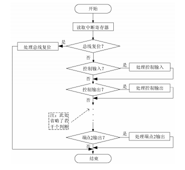
Figure 42 interrupt processing flow chart
The code for reading the interrupt register is as follows:
-- Read interrupt register status
when TS_READ_IR =>
    -- First step,Send command to read interrupt register
    if handle_step = 0 then
        a0 <= D12_COMMAND;
        data_out <= D12_COMMAND_READ_IR;
        wr_n_var := '0';
    -- Step two,Set the read signal to low,Read the first return parameter,First byte of interrupt register
    elsif handle_step = 1 then
        a0 <= D12_DATA;
        rd_n_var := '0';
    -- Step 3,Save the first byte of the interrupt register and read the second return parameter(Interrupt register second byte)
    elsif handle_step = 2 then
        -- Save the first byte of interrupt register
        ir_0 := data_in;
        -- Read the second parameter
        a0 <= D12_DATA;
        rd_n_var := '0';
        -- last,Save the second parameter,Enter the next processing state
    else
        -- Save the second byte of interrupt register
        ir_1 := data_in(0);
        -- Enter the next processing state according to the interrupt register selection
        ts_state <= GetInterruptHandler(ir_0, ir_1);
        ih_state <= IH_START;
    end if;
    handle_step := handle_step+1;
The following describes the processing flow of control output. The output of the control output is relative to the host, so relative to the device, it is to receive the data of the host. When a control output occurs, the device will first judge whether it has received a Setup Packet. If so, it will start to receive the following data. Otherwise, it will receive the remaining data from the previous transmission. The processing flow chart of control transmission is shown in Fig. 43.
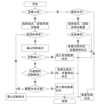
Figure 43 control output flow chart
As can be seen from the above flow chart, the device transceiver must first select the control output endpoint, extract the content of the establishment package, and then judge whether the endpoint is full or empty. If the control endpoint is not empty, the device transceiver will read the content from the buffer and save it. After that, it will judge the validity of the device request. If it is a valid request, the device transceiver must send a reply establishment command to the control output endpoint to re enable the next establishment stage.
Next, the device transceiver needs to confirm whether the control transmission controls reading or writing. This can be determined by reading the 8th bit of bmRequestType in the creation package. If the control transmission is a control read type, it means that the device needs to send back data packets to the host in the next data stage. The device transceiver will set a flag to indicate that the device is now in transmission mode, that is, it is ready to enter the transmission state (TS_EP0_TRANSMIT) to send data to the host when the host sends a request.
Each step of the processing flow is divided into two states in the device transceiver module, in which the operations of selecting endpoint and reading and saving data are in TS_ READ_ The endpoint state is implemented, and other contents are implemented in the TS_ EP0_ Implemented in receive state. The following is the implementation code read from the endpoint (buffer of PDIUSBD12), namely ts_ READ_ The code of endpoint status. Due to space reasons, only some reference codes are provided here.
-- Read endpoint data status
when TS_READ_ENDPOINT =>
    -- handle_step Indicates the operation steps
    case handle_step is
    -- first,Send select endpoint command,Select endpoint
    when 0 =>
        a0 <= D12_COMMAND;
        data_out <= active_ep;
        wr_n_var := '0';
        handle_step := handle_step+1;
    -- Send command to read endpoint data,Ready to receive data
    when 1 =>
        a0 <= D12_COMMAND;
        data_out <= D12_COMMAND_RW_BUFFER;
        wr_n_var := '0';
        handle_step := handle_step+1;
    -- Read the first two bytes of buffered data,The first byte is reserved data,The second byte represents the data length
    when 2 | 3 =>
        a0 <= D12_DATA;
        rd_n_var := '0';
        handle_step := handle_step+1;
    -- Save the second byte(Data length),Ready to receive valid data
    when 4 =>
        -- Reserve the second byte
        read_in := conv_integer(data_in);
        -- Judge whether the data length is zero
        if read_in = 0 then
            handle_step := 7;
        else
            -- Get remaining data
            handle_step := handle_step+1;
            a0 <= D12_DATA;
            rd_n_var := '0';
        end if;
    -- Read the data in turn and save the data
    when 5 =>
        -- Save the data required to be obtained in the previous cycle
        ts_data(ram_address) <= data_in;
        ram_address := ram_address+1;
        read_count := read_count+1;
        -- Judge whether all data has been obtained
        if read_count = read_in then
            handle_step := 6;
        else
            -- Continue to ask for the next data
            a0 <= D12_DATA;
            rd_n_var := '0';
        end if;
    -- last,Send command to clear endpoint buffer
    when 6 =>
        a0 <= D12_COMMAND;
        data_out <= D12_COMMAND_CLEAR_EP_BUFFER;
        wr_n_var := '0';
        handle_step := 7;
    -- Restore to original processing state
    when others =>
        handle_step := 0;
        ts_state <= last_ts_state;
    end case;
The following describes the processing process of control input. Control input is that the device sends data to the host, and the most typical is that the device sends descriptors to the host. Figure 44 shows the flow chart of control input.
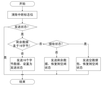
Figure 44 control input flow chart
It can be seen from the flow chart of control input that the device transceiver first needs to clear the interrupt flag bit by reading the last processing status register of PDIUSBD12. Then, the device transceiver sends the data packet after confirming that PDIUSBD12 is in the transmission mode. The control endpoint of PDIUSBD12 has only 16 byte FIFO. If the transmission length is greater than 16 bytes, the device transceiver must control the amount of data in the transmission stage. The device transceiver must check the current and remaining data size to be sent to the host. If the number of remaining bytes is greater than 16, the device transceiver will send 16 bytes first and continue to wait for the next transmission.
When the next data transmission interrupt comes, the device transceiver will determine whether the remaining bytes are zero. If there is no data to send, the device transceiver needs to send an empty packet to indicate that the host data has been sent.
The control input is in TS_EP0_TRANSMIT and TS_WRITE_ENDPOINT is implemented in two states. Where, TS_EP0_TRANSMIT implements control input process control, while TS_ WRITE_ Implementation of endpoint and TS_READ_ENDPOINT is very similar, except that read data is replaced by send data. TS_ WRITE_ The implementation code of endpoint status is as follows. Due to space reasons, only some reference codes are provided here.
-- Write endpoint cache data status
when TS_WRITE_ENDPOINT =>
    case handle_step is
    -- first,Send command to select endpoint,Select endpoint 0
    when 0 =>
        a0 <= D12_COMMAND;
        data_out <= active_ep;
        wr_n_var := '0';
        handle_step := handle_step+1;
    -- Reads a return parameter of the select endpoint command(Optional)
    when 1 =>
        a0 <= D12_DATA;
        rd_n_var := '0';
        handle_step := handle_step+1;
    -- Send command to read / write endpoint
    when 2 =>
        a0 <= D12_COMMAND;
        data_out <= D12_COMMAND_RW_BUFFER;
        wr_n_var := '0';
        handle_step := handle_step+1;
    -- Write the first byte of endpoint cache,Reserved bytes for,The value is 0
    when 3 =>
        a0 <= D12_DATA;
        data_out <= X"00";
        wr_n_var := '0';
        handle_step := handle_step+1;
    -- Write the second byte of endpoint cache,Valid data length is
    when 4 =>
        a0 <= D12_DATA;
        data_out <= conv_std_logic_vector(to_write, 8);
        wr_n_var := '0';
        write_count := 0;
        handle_step := handle_step+1;
    -- Write valid data sequentially
    when 5 =>
        if to_write = 0 then
            -- send comnand: enable buffer
            a0 <= D12_COMMAND;
            data_out <= D12_COMMAND_ENABLE_BUFFER;
            wr_n_var := '0';
            handle_step := 7;
        else
            handle_step := handle_step+1;
        end if;
    -- Send buffer valid command,allow PDIUSBD12 send data
    when 6 =>
        -- Determine whether all data has been written
        if write_count = to_write then
            --Send buffer valid command
            a0 <= D12_COMMAND;
            data_out <= D12_COMMAND_ENABLE_BUFFER;
            wr_n_var := '0';
            handle_step := 7;
          else
            -- Write data
            a0 <= D12_DATA;
            data_out <= ts_data(ram_address);
            ram_address := ram_address+1;
            wr_n_var := '0';
            write_count := write_count+1;
        end if;
    -- Restore to original processing state
    when 7 =>
        handle_step := 0;
        ts_state <= last_ts_state;
        when others =>
        NULL;
    end case;
The above is the implementation method of data access status. The above code can be tested in the test platform, and the input data during the test should be generated by the test platform (the preparation of the test platform will be specially introduced in the following chapters). For example, the simulation waveform of the device descriptor is sent for the first time. The simulation process can be divided into two parts. The first part (as shown in Figure 45) is the process of receiving the Setup Packet and reading the request data of PDIUSBD12; The second part (as shown in Figure 46) is to write the device descriptor data to the PDIUSBD12 endpoint cache and make the buffer valid.
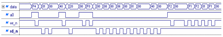
Fig. 45 simulation waveform 1 of transmitting device descriptor
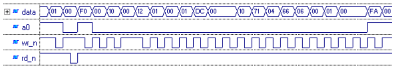
Fig. 46 simulation waveform 2 of transmitting device descriptor
3) Request reply status
The function of request reply status is to respond to each request. The standard request of USB has been introduced earlier. Now take the request for obtaining descriptor as an example to introduce the implementation method of request response. Other standard requests and manufacturer requests (obtaining and setting password) are relatively simple. Please refer to the source code for the implementation method.
The request to obtain the descriptor is the most important request, because it is necessary in the process of device enumeration. It is the first step for the host to understand the device. The processing flow of obtaining descriptor request is shown in Figure 47.
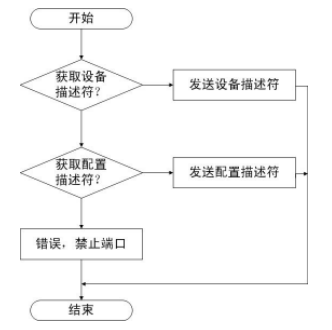
Fig. 47 process flow of acquiring descriptor
The implementation code for obtaining the device descriptor request response is as follows:
-- Get descriptor request response status
when TS_SEND_DESCRIPTOR =>
    handle_step := 0;
    active_ep := X"01";
    -- Determine whether it is a device request
        if ts_data(ADDRESS_DESCRIPTOR_TYPE) = TYPE_DEVICE_DESCRIPTOR then
            -- LED output,Prompt function
            led(0) <= '0';
            -- Check whether the data length meets the requirements
            if data_length > LENGTH_DEVICE_DESCRIPTOR then
                data_length := LENGTH_DEVICE_DESCRIPTOR;
            end if;
            -- Judge whether the descriptor length exceeds the cache size of endpoint 0
            if data_length > LENGTH_ENDPOINT0_BUFFER then
                to_write := LENGTH_ENDPOINT0_BUFFER;
                is_transmit := '1';
            else
                to_write := data_length;
            end if;
            -- Set transmission status flag bit,Set transmission data source(descriptor )And data length
            data_count := to_write;
            ram_address := ADDRESS_DEVICE_DESCRIPTOR;
            -- Ready to enter the control input state(TS_WRITE_ENDPOINT),send data
            ts_state <= TS_WRITE_ENDPOINT;
        elsif ts_data(ADDRESS_DESCRIPTOR_TYPE) = TYPE_CONFIGURATION_DESCRIPTOR then
            -- Check data length,LED output,Prompt function
            if data_length > LENGTH_CONFIGURATION_DESCRIPTOR then
                data_length := LENGTH_CONFIGURATION_DESCRIPTOR;
                led(2) <= '0';
            else
                led(1) <= '0';
            end if;
            -- Judge whether the descriptor length exceeds the cache size of endpoint 0
            if data_length > LENGTH_ENDPOINT0_BUFFER then
                to_write := LENGTH_ENDPOINT0_BUFFER;
                is_transmit := '1';
            else
                to_write := data_length;
            end if;
            -- Set transmission status flag bit,Set transmission data source(descriptor )And data length
            data_count := to_write;
            ram_address := ADDRESS_CONFIGURATION_DESCRIPTOR;
            -- Set transmission status flag bit,Set transmission data source(descriptor )And data length
            ts_state <= TS_WRITE_ENDPOINT;
        else
            ts_state <= TS_IDLE;
        end if;
        last_ts_state := TS_END_REQUESTHANDLER;
6.8 preparation of test platform
The above is the implementation method of the whole FPGA firmware system. In order to verify the correctness of the design, we also need to write a test platform to simulate the whole system. In practice, FPGA communicates with PDIUSBD12, so a virtual PDIUSBD12 is needed in the test platform to realize the purpose of simulation.
First of all, a virtual clock signal needs to be generated in the test platform. The generation method is to use the wait for statement to wait for a fixed time and flip the signal value. The implementation code of clock signal is as follows:
-- Clock signal generation code
clk_gen: process
begin
    -- Flip
    clk <= not clk;
    -- Wait a fixed time
    wait for 50 ns;
end process;
Secondly, since there is data reading and writing between FPGA and PDIUSBD12, it is necessary to simulate the data read from all FPGAs to PDIUSBD12. The method of analog data reading and writing is to write all data into a large test data array in order, use a variable as the index of the array, and then write a process sensitive to the read signal, send the data to the bus at the falling edge of each read signal, and increase several groups of index variables by 1. The definition method of test data array and index variable is as follows:
-- Test data array definition
signal td : REG256x8 :=
(
-- Get device descriptor test data for the first time
X"01", X"00", X"20", X"00", X"08", -- Each register data and the first two bytes of endpoint 0 cache
X"80", X"06", X"00", X"01", X"00", X"00", X"40", X"00", -- Get device descriptor request
X"00",
-- Set address request test data
X"01", X"00", X"20", X"00", X"08", -- Each register data and the first two bytes of endpoint 0 cache
X"00", X"05", X"02", X"00", X"00", X"00", X"00", X"00", -- Set address request
X"00",
-- Get complete device descriptor test data
X"01", X"00", X"20", X"00", X"08", -- Each register data and the first two bytes of endpoint 0 cache
X"80", X"06", X"00", X"01", X"00", X"00", X"12", X"00", -- Get configuration descriptor request
X"00",
X"02", X"00", X"00", X"00", -- Data of each register
-- Get configuration descriptor request test data
X"01", X"00", X"20", X"00", X"08", -- Each register data and the first two bytes of endpoint 0 cache
X"80", X"06", X"00", X"02", X"00", X"00", X"09", X"00", --Get configuration descriptor request
X"00",
--Get all configuration descriptor request test data
X"01", X"00", X"20", X"00", X"08", -- Each register data and the first two bytes of endpoint 0 cache
X"80", X"06", X"00", X"02", X"00", X"00", X"FF", X"00", -- Get configuration descriptor request
X"00",
X"02", X"00", X"00", X"00", -- Data of each register
X"02", X"00", X"00", X"00", -- Data of each register
-- Set configuration request test data
X"01", X"00", X"20", X"00", X"08", -- Each register data and the first two bytes of endpoint 0 cache
X"00", X"09", X"01", X"00", X"00", X"00", X"00", X"00", -- Set configuration request
X"00",
others => X"00"
);
-- Array index
signal td_index : INTEGER8 := 255;
Thirdly, we need to deal with the problem of bus dual drive. The function of the input / output selection module described above is to turn off the bus output when necessary to avoid the occurrence of double drive. Similarly, this should be done in the test platform, that is, when the test platform reads data from the FPGA firmware system, the bus output of the test platform should be turned off, that is, it should be set to high resistance. The implementation code is as follows:
process(d12_wr, td_index)
begin
    -- When FPGA towards PDIUSBD12 When some data,The bus output becomes high resistance
    if d12_wr = '0' then
        data <= "ZZZZZZZZ";
    else
        data <= td(td_index);
    end if;
end process;
Finally, a main process needs to be written. In the main process, system reset and interrupt signal need to be generated. The code is as follows:
-- main process
main: process
variable i : INTEGER8;
begin
    -- reset
    reset_n <= '0';
    wait for 100 ns;
    reset_n <= '1';
    wait for 100 us;
    -- Cyclic simulation generation PDIUSBD12 interrupt
    for i in 0 to 10 loop
        int_n_in <= '0';
        wait for 3200 ns;
        int_n_in <= '1';
        wait for 300 us;
    end loop;
    wait;
    end process;
7, USB driver and software development
7.1 USB driver programming
The above is the development process of FPGA firmware. Since the design in this example is not a class device, it is necessary to write special drivers and software to make the device work normally. Since drivers and software are not the focus of this article, the following is only a brief introduction to their writing methods.
1) USB driver model
The host software of USB system can be divided into two layers, namely USB system software and client driver, as shown in Figure 48.
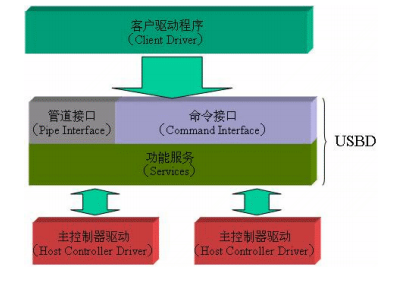
Figure 48 USB interface software model
USB system software can be divided into USBD and HCD according to its functions. HCD provides the abstraction of host controller and data transmission on the bus for the upper layer. USBD provides the abstraction of USB device for the upper client driver, and provides the abstraction of data transmission between the client driver and the driven device.
From the perspective of users, the client driver is equivalent to the driver in the traditional sense. However, different interfaces on the device side correspond to different drivers. If the device has only one interface, the two are the same from the user's point of view. The client driver interacts with the device through the interface provided by the USB system software, rather than through the past I/O address or port.
2) Using Driver Studio to develop USB driver
The above is the USB software model. For driver developers, what they need to write is the client driver. To write the client driver, we need to install ddk, namely Windows Driver Development Kit. Through ddk, we can access the interface of USB system software to realize the interaction with the device. However, if you only use DDK to develop drivers, it will be more complex, so you can use some special tools to drive development, such as Driver Studio, WinDriver, etc. This example uses Driver Studio 2.7 for development. The basic steps of development are described below. After installing DDK and Driver Studio, run the Driver Wizard of Driver Studio. In step 1, enter the name and path of the drive project, as shown in Figure 49. Click the Next button to enter the dialog box as shown in Figure 50.
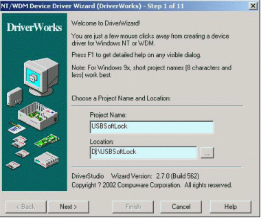
Figure 49 Driver Wizard step 1
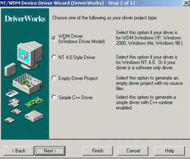
Figure 50 Driver Wizard step 2
Step 2 select the project type WDM Driver and click Next to enter the dialog box as shown in Figure 51.
Step 3 select the drive type WDM Function Driver. Click the Next button to enter the dialog box as shown in Figure 52.
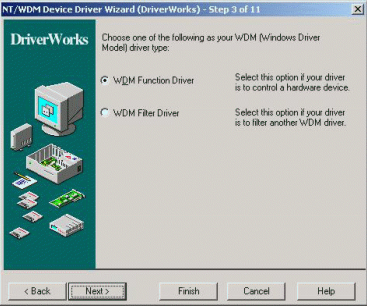
Figure 51 Driver Wizard step 3
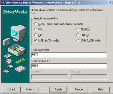
Figure 52 step 4 of driver wizard
Step 4 is important to select the type of drive bus. USB (WDM Only) should be selected, and note that the information consistent with the device description in the firmware should be entered in the USB Vendor ID and USB Product ID. Please note that the Vendor ID must be 0x0471 here, because the PDIUSBD12 chip of Philips is used, and its Vendor ID is fixed as 0x0471. Click the Next button to enter the dialog box as shown in Figure 53.
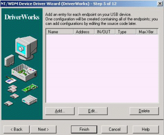
Figure 53 step 5 of driver wizard
Step 5 is endpoint definition. You can define the endpoint type (input / output), endpoint number, cache size, etc. as needed.
Steps 6 to 9 are the definitions of some development auxiliary information, which can be maintained as the default value, as shown in figures 54 to 57.
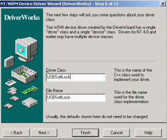
Figure 54 Driver Wizard step 6
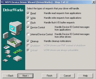
Figure 55 Driver Wizard step 7
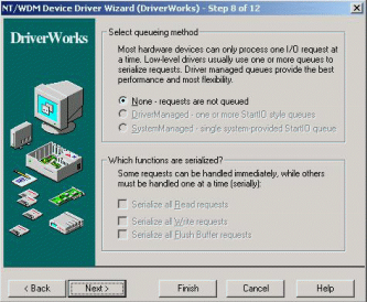
Figure 56 Driver Wizard step 8
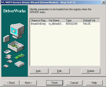
Figure 57 Driver Wizard step 9
Step 10 is the definition of the device class, as shown in Figure 58. Define the way to open the device. Symbolic Link means to open according to the device name, and Interface (WDM Only) means to open according to the GUID of the device. Here, choose to open using the device name.
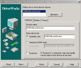
Figure 58 step 10 of driver wizard
Step 11 defines the IO control interface of the device, that is, the interface between the driver and the application program, as shown in Figure 59. Click the Add button to define the IO control interface, as shown in Figure 60.
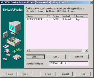
Figure 59 Driver Wizard step 11
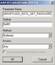
Figure 60 definition of IO control interface
Finally, step 12 makes some additional settings, as shown in Figure 61, which can keep the default values.
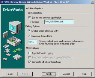
Figure 61 step 12 of driver wizard
The above is the complete process of using the Driver Wizard of Drive Studio to generate the driver framework. Now we have a code framework that completes most of the driving work. We only need to add some custom processing code.
3) Compiling drivers using Visual C + +
Run Visual C++ 6.0 to open the project file generated by the Driver Wizard. You can see that there are already many processing functions for Device operations in * * * Device class, such as ondevicepower up, ondevicessleep and OnDeviceStart. You can modify these functions as needed. If there are no special requirements, you can keep the default settings, As shown in Figure 62.

Operation function diagram 62
In addition, the work to be completed is to process the IO control interface function defined above, and its function is to establish a vendor request. Because the USB device designed this time is an encryption device, it is not a class device, so there will be some specific requests (manufacturer requests). In order to introduce the implementation method of manufacturer's request, the system uses two manufacturer's requests: setting password and obtaining password. Drivers automatically generated by the Driver Wizard generally include the establishment of standard requests, but will not include the establishment of manufacturer requests. The vendor request is established in the IO control interface function, that is, the two functions defined in step 11 of the Driver Wizard. The function to establish the vendor request is mainly the BuildVendorRequest function, and its format is as follows:
PURB BuildVendorRequest(
    PUCHAR TransferBuffer,
    ULONG TransferBufferLength,
    UCHAR RequestTypeReservedBits,
    UCHAR Request,
    USHORT Value,
    BOOLEAN bIn=FALSE,
    BOOLEAN bShortOk=FALSE,
    PURB Link=NULL
    UCHAR Index=0,
    USHORT Function=URB_FUNCTION_VENDOR_DEVICE,
    PURB pUrb=NULL
  );
Among them, the first six parameters need developers' attention, and their meanings are as follows:
• Puchar transferbuffer data buffer. If it is data input, it is used to store the received data; If it is data output, it is the data source of the data to be sent; If there is no data transmission, this parameter can be NULL.
• ULONG TransferBufferLength is the length of data sent or received.
• UCHAR RequestTypeReservedBit bit mask of the request type, which is generally zero.
• UCHAR Request code.
• USHORT Value is the wValue bit in the USB request
• BOOLEAN bIn=FALSE. If this parameter is TRUE, it indicates data output; otherwise, it indicates data input.
The remaining parameters can remain the default. Let's start with usbsoftlock_ IOCTL_ GET_ PASSWORD_ Take handler processing function as an example to introduce the usage of BuildVendorRequest function. The code is as follows:
NTSTATUS USBSoftLockDevice::USBSOFTLOCK_IOCTL_GET_PASSWORD_Handler(KIrp I)
{
    NTSTATUS status = STATUS_SUCCESS;
    // Output prompt information
    t << "Entering USBSoftLockDevice::USBSOFTLOCK_IOCTL_GET_PASSWORD_Handler, "
      << I << EOL;
    t << "IOctrlBuffer address is " << (LONG)(I.IoctlBuffer()) << EOL;
    t << "BufferedReadDest address is " << (LONG)(I.BufferedReadDest()) << EOL;
    t << "BufferedWriteSource address is " << (LONG)(I.BufferedWriteSource()) << EOL;
    t << "IoctlOutputBufferSize is " << (LONG)(I.IoctlOutputBufferSize()) << EOL;
    // Cache for storing 8-byte passwords
    UCHAR buffer[8];
    // Create a vendor request. The request code is REQUEST_GET_PASSWORD, data length 8
    PURB pUrb = m_Lower.BuildVendorRequest(
        buffer, -- Data buffer
        PASSWORD_LENGTH, -- Data length
        0, -- retain
        REQUEST_GET_PASSWORD, -- Request code
        0, -- Namely USB Requested wValue field
        TRUE -- TRUE Indicates data entry,Otherwise, it is data output
    );
    status = m_Lower.SubmitUrb(pUrb, NULL, NULL, OPERATION_TIMEOUT);
    // Judgment return value
    if (status == STATUS_SUCCESS) {
          t << "Received buffer is ";
          for (int i=0;i<PASSWORD_LENGTH;i++) {
              t << " " << buffer[i];
          }
          t << EOL;
          PUCHAR output_buffer = (PUCHAR)(I.IoctlBuffer());
          memcpy(output_buffer, buffer, PASSWORD_LENGTH);
    }
    else {
    }
    return status;
}
After completing the preparation of the manufacturer's request, you can compile the driver. There are two versions of driver compilation by default, namely Win32 Checked and Win32 Free. The former represents the debugging version and the latter represents the release version. Compared with the debugging version, the release version removes most of the debugging information and is relatively simplified.
The method of compiling driver is to open the toolbar CompuwareDriverStudio of Driver Studio in Visual C + +, as shown in Figure 63.
Figure 63 Compuware DriverStudio toolbar
Select the appropriate compiled version, and then click the last button of the Compuware DriverStudio toolbar. Please note that you cannot use the compile button of Visual C + + itself for driver compilation. The compilation is successful. If it is the Win32 Free version, the driver file usbsoftlock will be generated in the sys\objfre\i386 subdirectory of the project directory sys; If it is the Win32Checked version, the driver file will be in the sys\objchk\i386 subdirectory of the project directory. After the driver is successfully compiled, it is automatically generated by Driver Studio inf files (in the project directory) are placed in the same directory. When looking for the driver, you can specify this directory.
7.2 USB software preparation
Finally, it briefly introduces the compilation of USB software, that is, the implementation method of software access to USB devices.
USB software can access USB devices through USB driver. Writing USB software must comply with the interface specification defined by USB driver. Generally speaking, after using the Driver Wizard to generate a driver project, a * * * IOCTL will be generated at the same time H file, which is the bridge to establish the communication between software and driver. It defines the interface to access the driver, which needs to be referenced when writing software.
The writing of USB software generally has the following steps.
1) Turn on the device
To open a device, you need to call the CreateFile function, which treats the device as a file. The code is as follows:
BOOL CSoftLock::OpenDevice()
{
    if (m_hDevice != INVALID_HANDLE_VALUE)
        return TRUE;
    const char *sLinkName = "\\\\.\\USBSoftLockDevice0";
    m_hDevice = CreateFile(sLinkName,
          GENERIC_READ | GENERIC_WRITE,
          FILE_SHARE_READ,
          NULL,
          OPEN_EXISTING,
          0,
          NULL);
    return m_hDevice != INVALID_HANDLE_VALUE;
}
2) Call device IO interface
Call the device IO interface and use the DeviceIOControl function to control the device. The DeviceIOControl function is mainly used twice here, that is, setting password and obtaining password, which respectively correspond to the IO control interface function defined in the driver. For example, the calling method of setting password interface function is as follows:
BOOL CSoftLock::SetPassword(char* password)
{
// Note that Input and Output are named from the point of view
// of the DEVICE:
// bufInput supplies data to the device
// bufOutput is written by the device to return data to this application
    CHAR bufInput[IOCTL_INBUF_SIZE]; // Input to device
    CHAR bufOutput[IOCTL_OUTBUF_SIZE]; // Output from device
    ULONG nOutput; // Count written to bufOutput
    memset(bufInput, 0, BUFFER_LENGTH);
    memset(bufOutput, 0, BUFFER_LENGTH);
    memcpy(bufInput, password, PASSWORD_LENGTH);
    // Call device IO Control interface (USBSOFTLOCK_IOCTL_SET_PASSWORD) in driver
    printf("Issuing Ioctl to device - ");
    if (!DeviceIoControl( m_hDevice,
              USBSOFTLOCK_IOCTL_SET_PASSWORD,
              bufInput,
              PASSWORD_LENGTH,
              bufOutput,
              PASSWORD_LENGTH,
              &nOutput,
              NULL) )
    {
              printf("ERROR: DeviceIoControl returns %0x.", GetLastError());
              return FALSE;
    }
    else {
            printf("input buffer is : %s, output buffer is %s, output buffer size is %d",
                bufInput,
                bufOutput,
                nOutput);
    }
    return TRUE;
}
3) Turn off the device
Corresponding to opening the device, closing the device is to call the CloseHandle function to close the handle of the device, for example:
void CSoftLock::CloseIfOpen()
{
    if (m_hDevice != INVALID_HANDLE_VALUE)
    {
        // Close the handle to the driver
        if (!CloseHandle(m_hDevice))
        {
            printf("ERROR: CloseHandle returns %0x.\n", GetLastError());
        }
        m_hDevice = INVALID_HANDLE_VALUE;
    }
}
For the detailed code of USB software, please refer to the cube test program in the source code, which simulates the working process of a hardware encryption device. After the cube program runs, a cube will appear, making the cube rotate to indicate the normal running state of the program. The program needs a password to run, but the password is not saved on the computer, but on the USB device, and the password needs to be verified in time when the program runs. Once the password verification fails (possibly because the password is incorrect or the USB device is removed), the program will stop running. The method is to first select the menu file - > open device to open the USB device (as shown in Figure 64). If the device is successfully opened, select File - > play cube and enter the password in the password input box. If the password is correct, the cube will start to rotate, And the cube program checks the password with the USB device from time to time (you can see that the GOODLINK light of PDIUSBD12 will flash continuously, which indicates that there is data transmission). You can also set the password by selecting file - > Set Password, which will be sent to the device through the Set Password request.
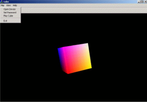
Figure 64 cube program running interface
summaryThis chapter first explains the architecture of USB system and the contents related to USB protocol. Then, it introduces the use method of USB interface device PDIUSBD12 in detail. Finally, this chapter describes the process of developing USB interface using FPGA interface PDIUSBD12 through an example. The learning points of this chapter can be summarized as follows:
First of all, the understanding of USB protocol is the most important. Although PDIUSBD12 chip can complete a lot of protocol analysis, the understanding of USB protocol plays a decisive role in the whole development process. USB protocol is very complex. The method of getting familiar with USB protocol should be from large to small, that is, first understand the basic principle of USB communication, such as the principle and characteristics of control transmission and batch transmission; Then understand the composition of each transmission, that is, what data packet is sent first and what data packet is received by each transmission; Finally, analyze the format and significance of each data packet.
Secondly, we need to know more about PDIUSBD12 chip, such as the functions and characteristics of its signal pins, and more importantly, its communication timing and control commands.
Finally, familiarity with various languages and development tools is also very important. In this design, many development languages need to be used, including VHDL, C + + (Visual C + +); In addition, this design also uses a variety of development tools, including EDA development, driver development, software development, etc. only when you are familiar with these tools can you develop quickly. USB system is very huge, so this chapter is also written to help readers step into the door of USB development. I hope readers can design a more perfect and efficient USB interface through the study of this chapter.
This is the end of this article. Great Xia, goodbye! ENDThe follow-up will be continuously updated, bringing installation related design tutorials such as Vivado, ISE, Quartus II and candence, learning resources, project resources, good article recommendations, etc. I hope you will continue to pay attention.
Heroes, the Jianghu is so big. Continue to wander. May everything be well. See you again!