This article is my experience after participating in the Blue Bridge Cup embedded competition and some of my own summary of the driver code, hoping to bring some help to the students who participate in the Blue Bridge Cup embedded in the future.
This article has not been proofread. If there are any mistakes, please forgive them. Welcome to exchange and correct. Please indicate the source of reprint.
Blue Bridge Cup match point data package
1, Summary
Own situation:
I participated in the 10th Blue Bridge Cup embedded competition
Two weeks of provincial competition preparation (4-6 hours per day on average), and the last provincial one enters the national competition
One and a half weeks of national preparation (write a provincial or national event every night), and the last national one
Those who have studied stm32 before can get started quickly (don't worry about it here, it doesn't matter if you have the experience of using stm32)
Then talk about the understanding of the embedded competition of the Blue Bridge Cup:
I don't think it's easy to win the prize in this competition, but it's difficult to win the first prize or above in China. You need some training and some luck. For example, I needed to write 18b20 read functions by myself, which happened to be memorized by me, and then I was lucky enough to write them. Officially, he only gave the underlying driver, such as i2c read function, write function, stop function and start function. At that time, he didn't read and write 24c02 function for you. At this time, you are the only one who wrote 24c02 read and write function
The investigation scope of the competition is limited and basically all routines. If you master all the limited knowledge and routines, you can get the second place in China. I will also sort out all the points you need to master in the next article
This competition is mainly aimed at students majoring in electronic engineering and students majoring in computer science. If they are not students majoring in electronic engineering, they need to supplement some basic knowledge (C language, microcomputer principle, digital, electronic, analog, etc.) )
The competition is mainly for non school students. It mainly focuses on the use of stm32 (after all, the program question accounting for 70% of the total score is to write a small program). Secondly, in the objective question, it will investigate some basic knowledge of stm32, Cortex-M3, embedded, digital analog electricity (especially the core of Cortex-M3)
What will I conclude:
I think we must master the driving force and its application
How to quickly complete our program through the information provided by the competition
My personal experience of the investigation site and how to allocate our preparation time
Preparation of objective questions
And a series of objective questions
PS:
The biggest advantage and disadvantage of this competition is that the scope of investigation is limited
By the way, this embedded development software can only be keil 4 and keil 5 can't be downloaded. So you have to install keil 4. I use keil 4.73, and the game version seems to be 4.73.
Keil 4.73 download link: Click to enter
After reading this article and mastering what I mentioned, at least one can be saved. Welcome to exchange and share, do not commercial oh.
2, Match offer
All children's shoes will definitely ask what to provide during the competition, which is not well explained on the official website. Here I will explain:
2.1 provided by provincial competition
2.1.1 hardware of provincial competition
Provincial competitions only provide competition boards, and do not involve the contents of expansion boards
2.1.2 software of provincial competition
Information chart provided by provincial competition:

Download link: Click to download
2.1.2.1 circuit schematic diagram and instruction of ct117e (competition board)
If you forget the pin corresponding to the resource on the board during the game, the circuit schematic is used to view the corresponding pin.
2.1.2.2 serial port debugging tools
The first thing to do after entering the examination room is to check whether the FT2232 on board is available after being plugged in, whether the program can be downloaded, whether the serial port can be used, especially whether the program can be downloaded
2.1.2.3 data sheet of data manual:
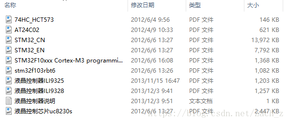
These data manuals have different uses. I think the most useful stm32f103rbt6.pdf, how to read the data manual and when to read it will be discussed later. Other commonly used ones need to be memorized, such as 24c02. I used them in provincial competitions
2.1.2.4 LCD drive reference routine
LCD drive reference history: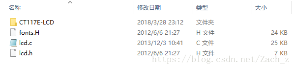
- A written project CT117E-LCD: this project can be used to test whether the board and screen work normally when we enter the examination room, or to build our program directly on this project, which omits the time for us to rebuild the project (I choose to rebuild the project), so don't do stupid things, to build a new project by ourselves, and it won't cost us time.
- lcd driver files: one. c source file and two. h header files. These three are lcd driver files. How to use them will be discussed later
2.1.2.5 i2c reference procedure
Only i2c.c and i2c.h files can be used for E2PROM and gyroscope. How to use them will be discussed later
2.1.2.6 STM32 firmware library v3.5
Firmware library data:
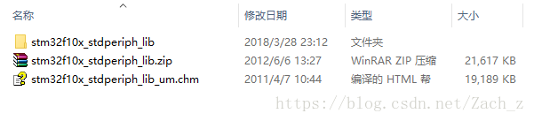
This firmware library is very critical. As long as you can make good use of the library functions and examples in it, you can quickly write drivers
2.2 provided by National Games
On hardware: competition board + expansion board
On the basis of all the information provided by the provincial competition, the national competition has added:
Related data manual and circuit schematic diagram of expansion board
Drivers of DS18B20 and DHT11
- Only. c and. h files, no project and demo, and no read function
3, Fast writing essential drivers
First of all, I will tell you that this competition doesn't depend on the layout of your program, so I will put all the programs in the main, so as to save time, as long as every function is encapsulated well, it won't make me dizzy. Especially in the national competition, the amount of questions is very large. I still have a little problem to solve in the end, so we have to save time The function of each module will be put on the main() function, so we do not need to define this step. Can make our development faster.
Now I start to write. With the help of firmware library fast write driver method, all our reference files are from the STM32 firmware library v3.5 \ stm32f110x \ stdperiph \ lib \ stm32f10x \ stdperiph \ lib \ v3.5.0 \ project \ stm32f10x \ stdperiph \ examples directory
3.1LED driver
In the V3.5 library provided by the competition, under the folder "project - > stm32f10x ﹣ stdperiph ﹣ examples - > GPIO - > iotoggle", open "main.c"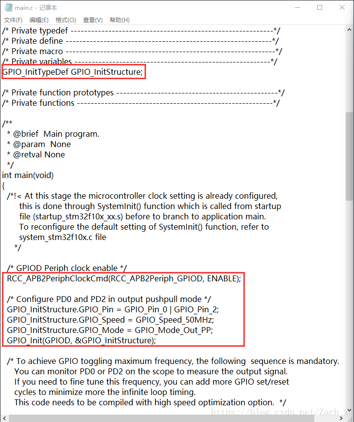
/***********************************************
*****************LED****************************
************************************************/
void led_init()
{
    GPIO_InitTypeDef GPIO_InitStructure;

    RCC_APB2PeriphClockCmd(RCC_APB2Periph_GPIOC|RCC_APB2Periph_GPIOD, ENABLE);

  /* Configure PD0 and PD2 in output pushpull mode */
  GPIO_InitStructure.GPIO_Pin = 0XFF00;//In stm, io is bitwise
  //This writing is equivalent to selecting GPIO ﹣ pin 8-15
  GPIO_InitStructure.GPIO_Speed = GPIO_Speed_50MHz;
  GPIO_InitStructure.GPIO_Mode = GPIO_Mode_Out_PP;
  GPIO_Init(GPIOC, &GPIO_InitStructure);

  GPIO_InitStructure.GPIO_Pin = 0X0004;
  GPIO_Init(GPIOD, &GPIO_InitStructure);

    GPIO_SetBits(GPIOC,0XFF00);    //Pc 8-15
    GPIO_SetBits(GPIOD,0X0004); //pd2
    GPIO_ResetBits(GPIOD,0x0004);      //pd2
}

u16 led_data=0xff00;//Save last light status
void led_one(u8 led,_Bool Flag)
{
    GPIO_SetBits(GPIOC,led_data);
    led=led+7;

    if(Flag)    GPIO_ResetBits(GPIOC,1<<led);
    else     GPIO_SetBits(GPIOC,1<<led);

    GPIO_SetBits(GPIOD,0X0004);
    GPIO_ResetBits(GPIOD,0x0004);
    led_data=GPIO_ReadOutputData(GPIOC);
}
3.2key key drive
There are two ways to drive the key,
- External interrupt
- Circular scan
Here I recommend using external interrupt, because the response is fast, but it's better to learn both, otherwise it's cool if you can't use external interrupt
3.2.1 external interruption method
Here we need to know how the external interrupt service function of 32 is allocated
Here, exti0-4 has independent interrupt service functions, which can be seen in startup ﹣ stm32f10x ﹣ md.s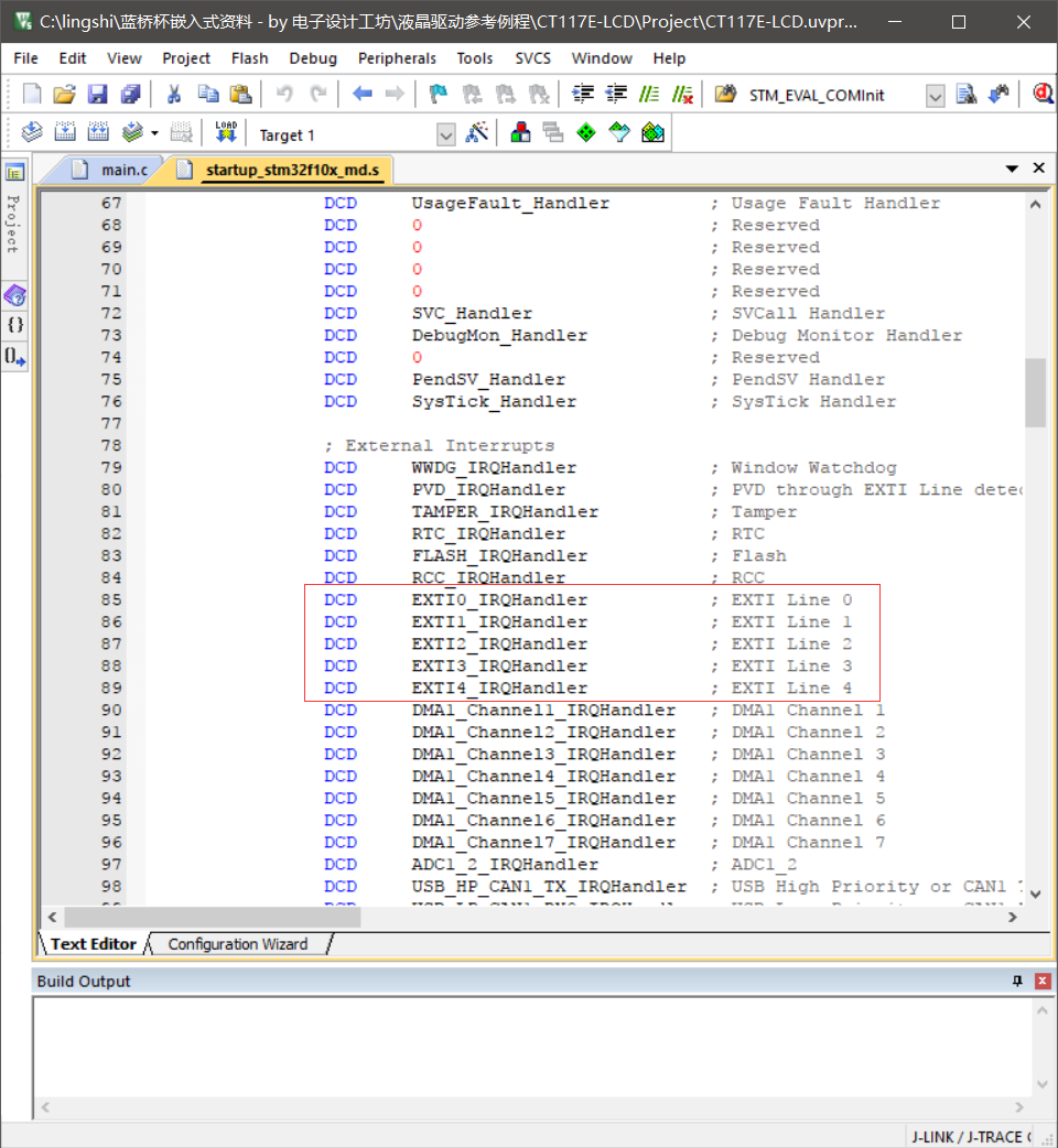
                DCD     EXTI0_IRQHandler           ; EXTI Line 0
                DCD     EXTI1_IRQHandler           ; EXTI Line 1
                DCD     EXTI2_IRQHandler           ; EXTI Line 2
                DCD     EXTI3_IRQHandler           ; EXTI Line 3
                DCD     EXTI4_IRQHandler           ; EXTI Line 4
exti9-5 is a combined interrupt service function, in which you need to determine which external interrupt caused the response event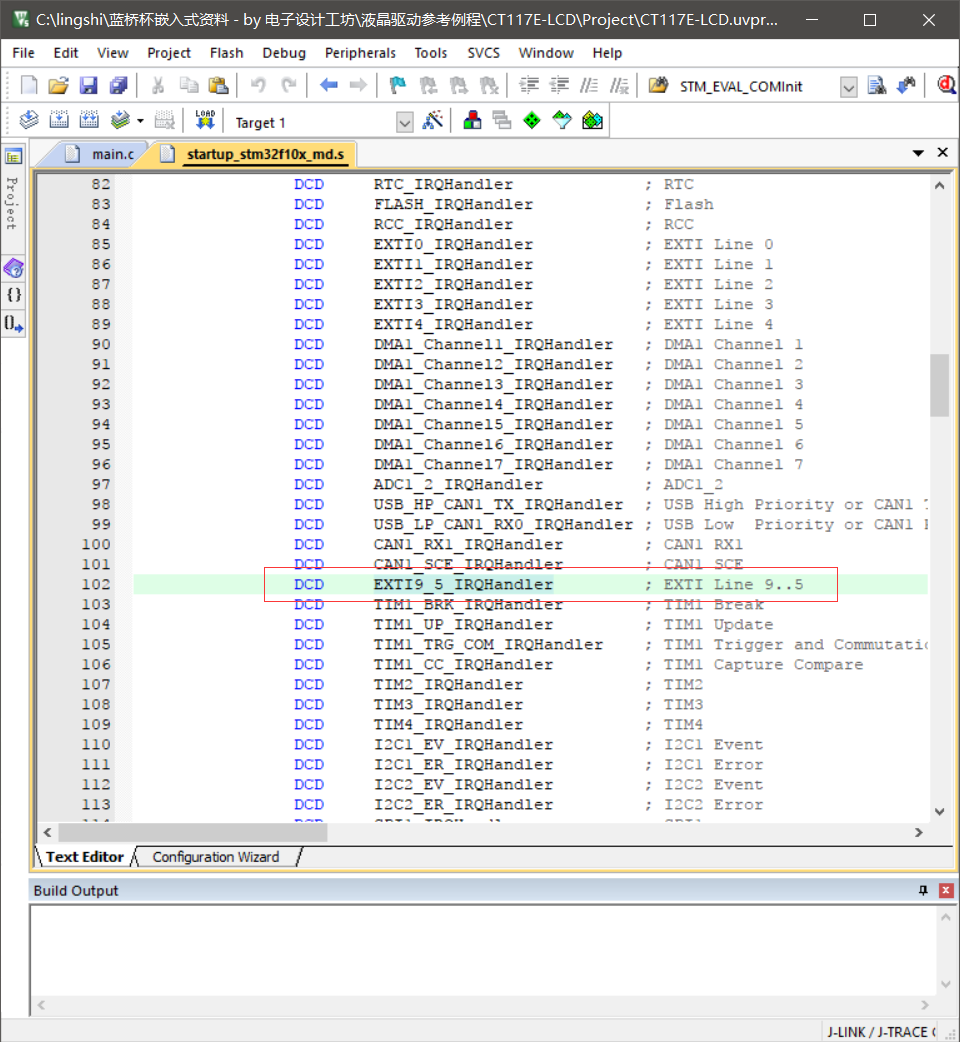
exti15-10 is a combined interrupt service function, and it is also necessary to determine which interrupt service function is responding to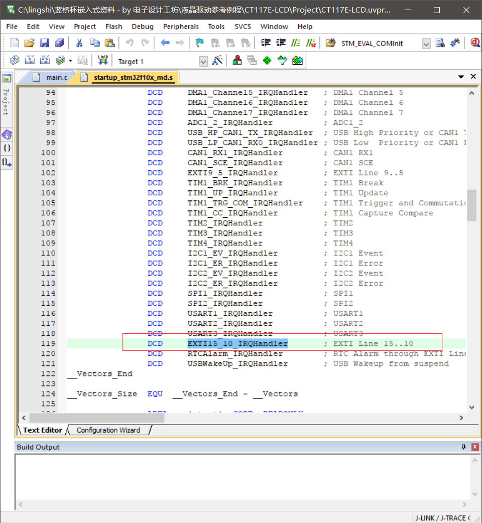
Then the interrupt service function corresponds to io
| GPIO | Interrupt service function |
|---|---|
| GPIO0 | exti0 |
| GPIO1 | exti1 |
| ... | ... |
| GPIO5 | exti9-5 |
| GPIO6 | exti9-5 |
| ... | exti9-5 |
| GPIO10 | exti15-10 |
| GPIO11 | exti15-10 |
| ... | exti15-10 |
| GPIO15 | exti15-10 |
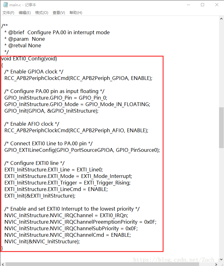
In the V3.5 library provided by the competition, open "main.c" under the folder "project - > stm32f10" ﹣ stdperiph ﹣ examples - > exti - > exti ﹣ config ":
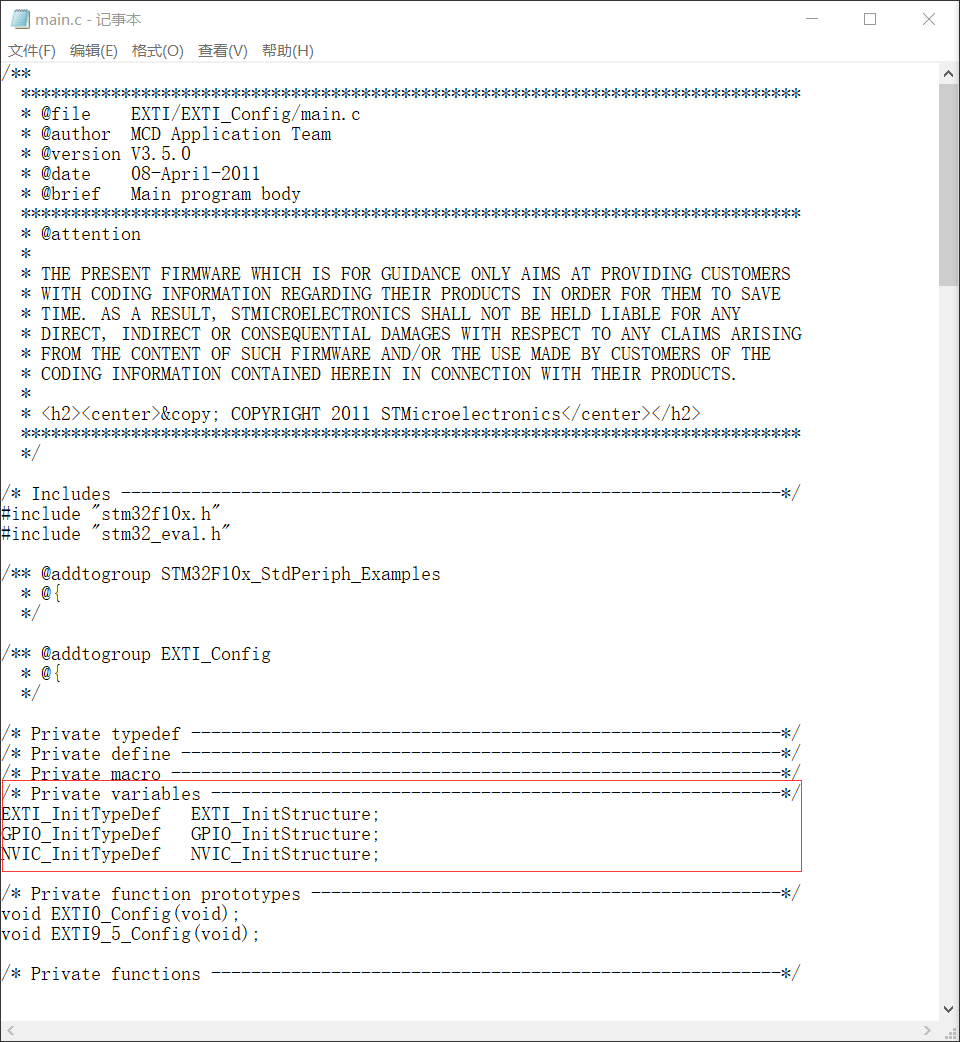
Then open "stm32f10x it. C" under "exti" config ":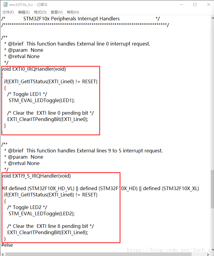
/*************************************************************
***************************EXTI********************************
**************************************************************/
u8 key_value=0;
void EXTI0_Config(void)
{
    EXTI_InitTypeDef   EXTI_InitStructure;
    GPIO_InitTypeDef   GPIO_InitStructure;
    NVIC_InitTypeDef   NVIC_InitStructure;
  /* Enable GPIOA clock */
  RCC_APB2PeriphClockCmd(RCC_APB2Periph_GPIOA|RCC_APB2Periph_GPIOB, ENABLE);

  /* Configure PA.00 pin as input floating */
  GPIO_InitStructure.GPIO_Pin = GPIO_Pin_0|GPIO_Pin_8;
  GPIO_InitStructure.GPIO_Mode = GPIO_Mode_IN_FLOATING;
  GPIO_Init(GPIOA, &GPIO_InitStructure);

    GPIO_InitStructure.GPIO_Pin = GPIO_Pin_1|GPIO_Pin_2;
  GPIO_Init(GPIOB, &GPIO_InitStructure);


  /* Enable AFIO clock */
  RCC_APB2PeriphClockCmd(RCC_APB2Periph_AFIO, ENABLE);

  /* Connect EXTI0 Line to PA.00 pin */
  GPIO_EXTILineConfig(GPIO_PortSourceGPIOA, GPIO_PinSource0);

  /* Configure EXTI0 line */
  EXTI_InitStructure.EXTI_Line = EXTI_Line0;
  EXTI_InitStructure.EXTI_Mode = EXTI_Mode_Interrupt;
  EXTI_InitStructure.EXTI_Trigger = EXTI_Trigger_Rising;
  EXTI_InitStructure.EXTI_LineCmd = ENABLE;
  EXTI_Init(&EXTI_InitStructure);

  /* Enable and set EXTI0 Interrupt to the lowest priority */
  NVIC_InitStructure.NVIC_IRQChannel = EXTI0_IRQn;
  NVIC_InitStructure.NVIC_IRQChannelPreemptionPriority = 0x0F;
  NVIC_InitStructure.NVIC_IRQChannelSubPriority = 0x0F;
  NVIC_InitStructure.NVIC_IRQChannelCmd = ENABLE;
  NVIC_Init(&NVIC_InitStructure);


  /* Connect EXTI8 Line to PG.08 pin */
  GPIO_EXTILineConfig(GPIO_PortSourceGPIOA, GPIO_PinSource8);
  /* Configure EXTI8 line */
  EXTI_InitStructure.EXTI_Line = EXTI_Line8;
  EXTI_Init(&EXTI_InitStructure);

  /* Enable and set EXTI9_5 Interrupt to the lowest priority */
  NVIC_InitStructure.NVIC_IRQChannel = EXTI9_5_IRQn;
  NVIC_Init(&NVIC_InitStructure);


  /* Connect EXTI8 Line to PG.08 pin */
  GPIO_EXTILineConfig(GPIO_PortSourceGPIOB, GPIO_PinSource1);
  /* Configure EXTI8 line */
  EXTI_InitStructure.EXTI_Line = EXTI_Line1;
  EXTI_Init(&EXTI_InitStructure);
  /* Enable and set EXTI9_5 Interrupt to the lowest priority */
  NVIC_InitStructure.NVIC_IRQChannel = EXTI1_IRQn;
  NVIC_Init(&NVIC_InitStructure);

  /* Connect EXTI8 Line to PG.08 pin */
  GPIO_EXTILineConfig(GPIO_PortSourceGPIOB, GPIO_PinSource2);
  /* Configure EXTI8 line */
  EXTI_InitStructure.EXTI_Line = EXTI_Line2;
  EXTI_Init(&EXTI_InitStructure);
  /* Enable and set EXTI9_5 Interrupt to the lowest priority */
  NVIC_InitStructure.NVIC_IRQChannel = EXTI2_IRQn;
  NVIC_Init(&NVIC_InitStructure);
}

void EXTI0_IRQHandler(void)
{
  if(EXTI_GetITStatus(EXTI_Line0) != RESET)
  {
        key_value=1;
    /* Clear the  EXTI line 0 pending bit */
    EXTI_ClearITPendingBit(EXTI_Line0);
  }
}

/**
  * @brief  This function handles External lines 9 to 5 interrupt request.
  * @param  None
  * @retval None
  */
void EXTI9_5_IRQHandler(void)
{
  if(EXTI_GetITStatus(EXTI_Line8) != RESET)
  {
        key_value=2;
    /* Clear the  EXTI line 8 pending bit */
    EXTI_ClearITPendingBit(EXTI_Line8);
  }
}

void EXTI1_IRQHandler(void)
{
  if(EXTI_GetITStatus(EXTI_Line1) != RESET)
  {
        key_value=3;
    /* Clear the  EXTI line 0 pending bit */
    EXTI_ClearITPendingBit(EXTI_Line1);
  }
}

void EXTI2_IRQHandler(void)
{
  if(EXTI_GetITStatus(EXTI_Line2) != RESET)
  {
        key_value=4;
    /* Clear the  EXTI line 0 pending bit */
    EXTI_ClearITPendingBit(EXTI_Line2);
  }
}
3.2.2 key key cycle scanning
This one needs to be written by myself. This one is written by myself. It's very simple and fast.
void key_init()
{
  GPIO_InitTypeDef GPIO_InitStructure;

	RCC_APB2PeriphClockCmd(RCC_APB2Periph_GPIOA | RCC_APB2Periph_GPIOB ,ENABLE);

	GPIO_InitStructure.GPIO_Pin = GPIO_Pin_0|GPIO_Pin_8;
  GPIO_InitStructure.GPIO_Mode = GPIO_Mode_IPD;
  GPIO_InitStructure.GPIO_Speed = GPIO_Speed_50MHz;

  GPIO_Init(GPIOA, &GPIO_InitStructure);

	GPIO_InitStructure.GPIO_Pin = GPIO_Pin_1|GPIO_Pin_2;
  GPIO_Init(GPIOB, &GPIO_InitStructure);
}

uint8_t key_data_out=0;
void key_data()
{
	if(GPIO_ReadInputDataBit(GPIOA,GPIO_Pin_0)==0)
	{
		Delay_Ms(10);
		if(GPIO_ReadInputDataBit(GPIOA,GPIO_Pin_0)==0)
		{
			key_data_out=1;
			while(GPIO_ReadInputDataBit(GPIOA,GPIO_Pin_0)==0);
		}
	}
	else if(GPIO_ReadInputDataBit(GPIOA,GPIO_Pin_8)==0)
	{
		Delay_Ms(10);
		if(GPIO_ReadInputDataBit(GPIOA,GPIO_Pin_8)==0)
		{
			key_data_out=2;
			while(GPIO_ReadInputDataBit(GPIOA,GPIO_Pin_8)==0);
		}
	}
	else if(GPIO_ReadInputDataBit(GPIOB,GPIO_Pin_1)==0)
	{
		Delay_Ms(10);
		if(GPIO_ReadInputDataBit(GPIOB,GPIO_Pin_1)==0)
		{
			key_data_out=3;
			while(GPIO_ReadInputDataBit(GPIOB,GPIO_Pin_1)==0);
		}
	}
	else if(GPIO_ReadInputDataBit(GPIOB,GPIO_Pin_2)==0)
	{
		Delay_Ms(10);
		if(GPIO_ReadInputDataBit(GPIOB,GPIO_Pin_2)==0)
		{
			key_data_out=4;
			while(GPIO_ReadInputDataBit(GPIOB,GPIO_Pin_2)==0);
		}
	}
	else 	key_data_out=0;
}
3.3 serial port drive
If there is a problem with initialization, first check whether the port is open. Sometimes if the serial port fails, move the initialization position,
Under the folder "project - > stm32f10x ﹣ stdperiph ﹣ examples - > USART - > interrupt", open "main.c":
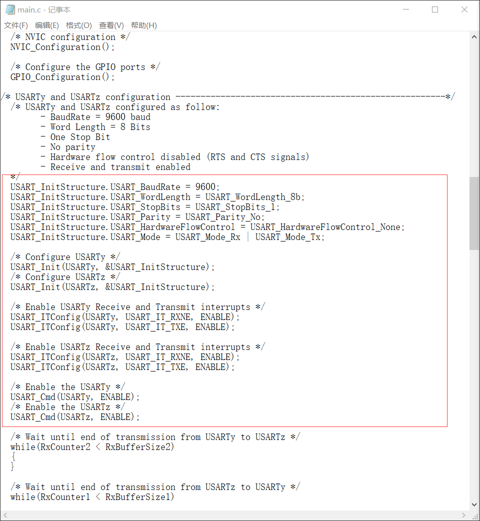
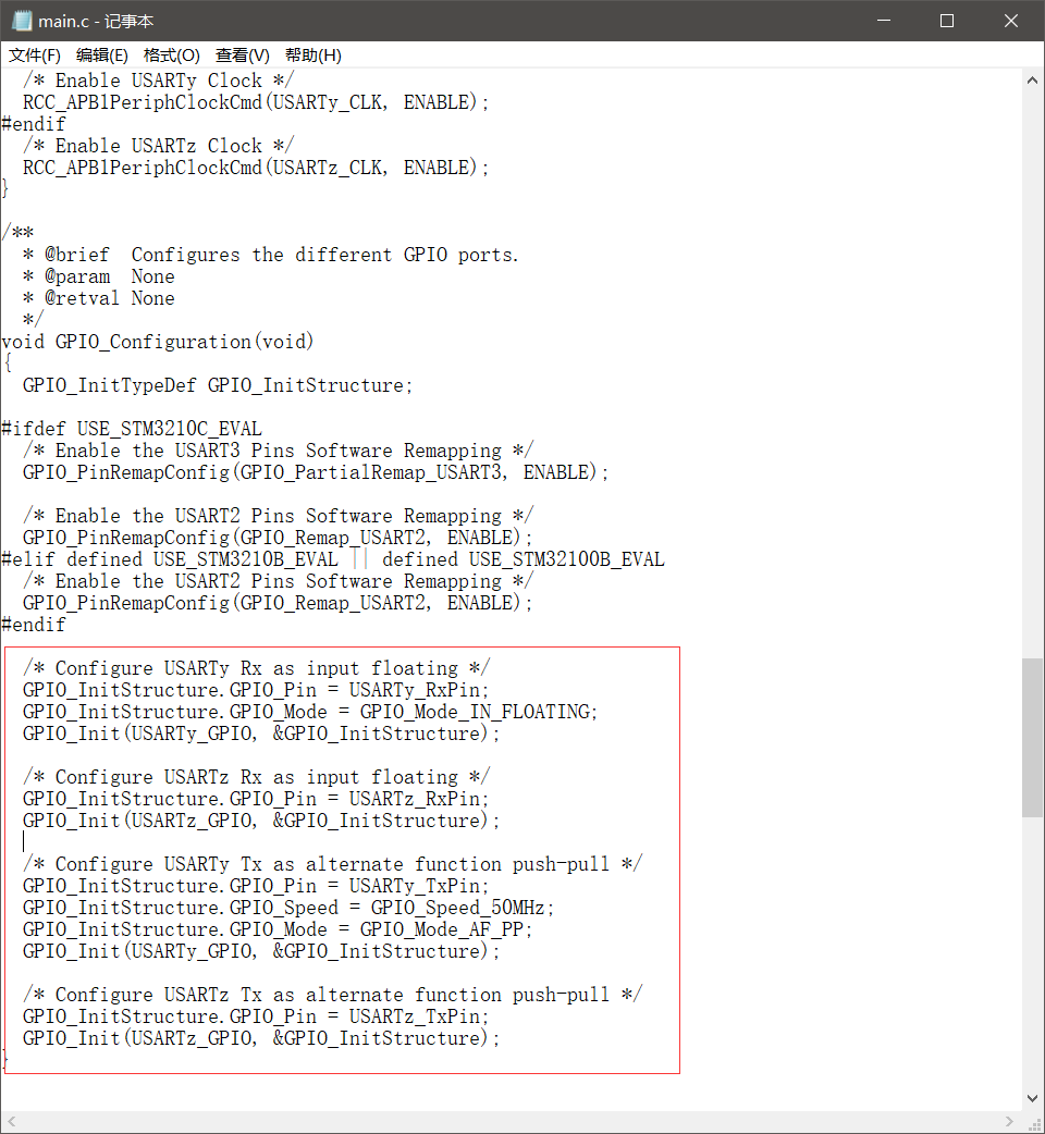
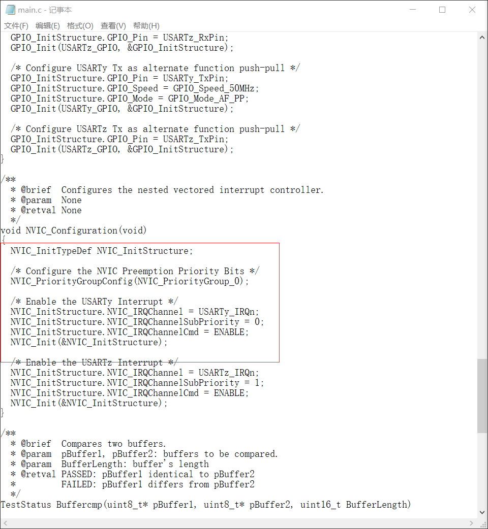
Change the receiving pin to PA3, the sending pin to PA2, the interrupt IRQChannel to usart2 ﹣ IRQN, and then enable the corresponding clock.
Open "stm32f10x it. C" in the same directory to find the code related to receiving interrupt function: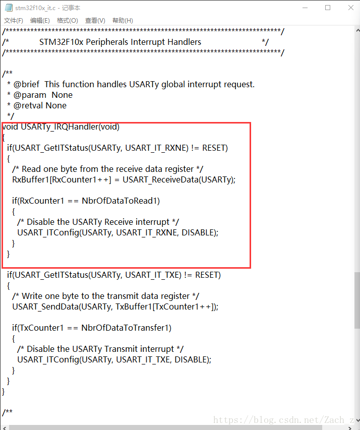
Then open the main.c function in the USART - > printf directory to find the sending function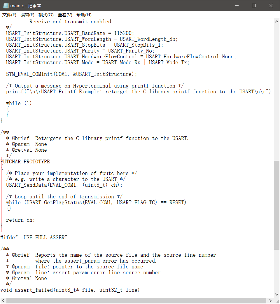
/*********************************************************************
************************Serial port*****************************************
******************************************************************/
void usart_Init()
{
    USART_InitTypeDef USART_InitStructure;
    GPIO_InitTypeDef GPIO_InitStructure;
    NVIC_InitTypeDef NVIC_InitStructure;

    RCC_APB2PeriphClockCmd(RCC_APB2Periph_AFIO, ENABLE);
    RCC_APB1PeriphClockCmd(RCC_APB1Periph_USART2,ENABLE);

    GPIO_InitStructure.GPIO_Pin = GPIO_Pin_3;
    GPIO_InitStructure.GPIO_Mode = GPIO_Mode_IN_FLOATING;
    GPIO_Init(GPIOA, &GPIO_InitStructure);

 	GPIO_InitStructure.GPIO_Pin = GPIO_Pin_2;
    GPIO_InitStructure.GPIO_Speed = GPIO_Speed_50MHz;
    GPIO_InitStructure.GPIO_Mode = GPIO_Mode_AF_PP;
    GPIO_Init(GPIOA, &GPIO_InitStructure);

	NVIC_InitStructure.NVIC_IRQChannel = USART2_IRQn;
    NVIC_InitStructure.NVIC_IRQChannelSubPriority = 1;
	NVIC_InitStructure.NVIC_IRQChannelPreemptionPriority=2;
    NVIC_InitStructure.NVIC_IRQChannelCmd = ENABLE;
    NVIC_Init(&NVIC_InitStructure);

    USART_InitStructure.USART_BaudRate = 9600;
    USART_InitStructure.USART_WordLength = USART_WordLength_8b;
    USART_InitStructure.USART_StopBits = USART_StopBits_1;
    USART_InitStructure.USART_Parity = USART_Parity_No;
    USART_InitStructure.USART_HardwareFlowControl = USART_HardwareFlowControl_None;
    USART_InitStructure.USART_Mode = USART_Mode_Rx | USART_Mode_Tx;

    USART_Init(USART2, &USART_InitStructure);

    USART_ITConfig(USART2, USART_IT_RXNE, ENABLE);

    USART_Cmd(USART2, ENABLE);
}

/*The change is the putchar? Prototype function in USART\printf\main*/
void usart_data_while(u8* ch)
{
    while(*ch)
    {
        /* Place your implementation of fputc here */
        /* e.g. write a character to the USART */
        USART_SendData(USART2, (uint8_t) *ch++);

        /* Loop until the end of transmission */
        while (USART_GetFlagStatus(USART2, USART_FLAG_TXE) == RESET)
        {}

    }
}


uint8_t RxBuffer1[20];
__IO uint8_t RxCounter1;
void USART2_IRQHandler(void)
{
  if(USART_GetITStatus(USART2, USART_IT_RXNE) != RESET)
  {
    /* Read one byte from the receive data register */
    RxBuffer1[RxCounter1++] = USART_ReceiveData(USART2);

    if(RxCounter1 == 20)
    {
      RxCounter1=0;
    }
  }
}
3.4 driver of E2PROM
3.4.1 software driver of E2PROM
Directly copy and paste "i2c.c" and "i2c.h" provided by the competition into the HARDWARE folder in our project directory, and add i2c.c to the project
Add the reading and writing driver code of E2PROM to i2c.c:
void x24_write(u8 add,u8 data)
{
I2CStart();
I2CSendByte(0xa0);
I2CWaitAck();

I2CSendByte(add);
I2CWaitAck();

I2CSendByte(data);
I2CWaitAck();

I2CStop();
Delay_Ms(3);
}
u8 x24_read(u8 add)
{
u8 data;
I2CStart();

I2CSendByte(0xa0);
I2CWaitAck();

I2CSendByte(add);
I2CWaitAck();

I2CStart();
I2CSendByte(0xa1);
I2CWaitAck();

data=I2CReceiveByte();
I2CSendAck();

Delay_Ms(3);
return data;
}
It should be noted here that a delay function (I delay 3ms) needs to be added after each read or write, because the internal execution speed of MCU is too fast, and the E2PROM peripheral cannot keep up with the internal clock frequency. If the MCU runs too fast and the peripheral response fails to keep up, the data will start to increase automatically before the data in E2PROM is obtained, resulting in the expected result of the program is not the same as the actual execution result.
3.4.2 reading and writing a u32 type data
During the competition, we will not only read and write a Byte of data, but also read and write int type or float type data, so it is very important to use flexibly according to the driver of reading and writing a Byte of data.
Reading and writing data of type u32
void x24_write_int(u8 add, int data)
{
	x24_write(add,(u8)(data&0xff));
	delay_ms(2);
	x24_write(add+1,(u8)(data>>8&0xff));
	delay_ms(2);
	x24_write(add+2,(u8)(data>>16&0xff));
	delay_ms(2);
	x24_write(add+3,(u8)(data>>24&0xff));
	delay_ms(2);
}

int x24_read_int(u8 add)
{
	int data;
	data=(int)x24_read(add);
	delay_ms(2);
	data+=(int)x24_read(add+1)<<8;
	delay_ms(2);
	data+=(int)x24_read(add+2)<<16;
	delay_ms(2);
	data+=(int)x24_read(add+3)<<24;
	delay_ms(2);
	return data;
}
3.4.3 driving with E2PROM
First of all, we need to initialize i2c when the main function is initialized, and then use the read function to read out the data we need. If we want to write, we can write the data directly.
#include "i2c.h"
u32 test_int=0;
int main()
{
    i2c_init();
    if(x24_read_int(0x55)==0x55)//Determine whether to write for the first time. If it is the first time, write
    {
    	 x24_write(0x55,0x55);
   		 test_int=x24_read_int(0x01);
    }
    while(1)
    {
        ...
    }

}
3.5 clock completion with RTC
In the V3.5 library provided by the competition, open "main.c" under the folder "project - > stm32f10" ﹣ stdperiph ﹣ examples - > RTC - > LSI ﹣ calib ":
Copy and paste the RTC configuration() part directly. Remember not to use the last two sentences. We don't have batteries, so there is no backup,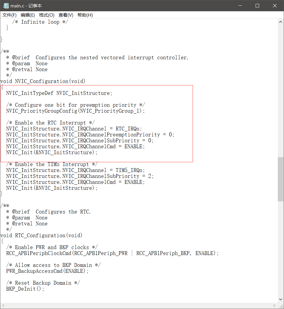
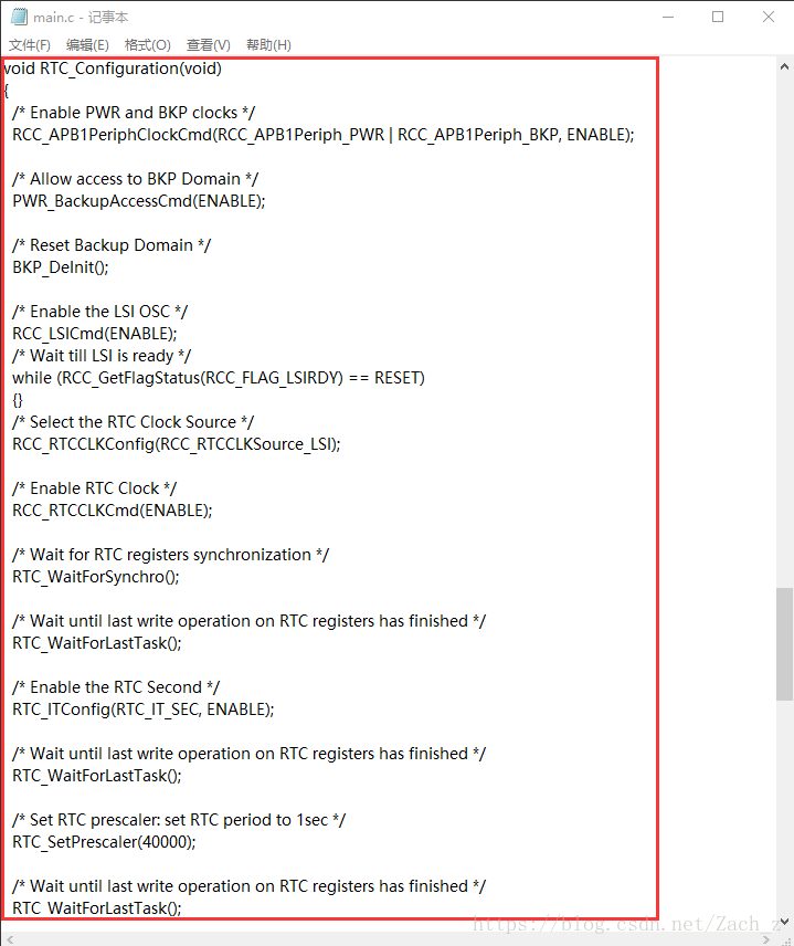
void RTC_Configuration(void)
{
    NVIC_InitTypeDef NVIC_InitStructure;

  /* Configure one bit for preemption priority */
  NVIC_PriorityGroupConfig(NVIC_PriorityGroup_1);

  /* Enable the RTC Interrupt */
  NVIC_InitStructure.NVIC_IRQChannel = RTC_IRQn;
  NVIC_InitStructure.NVIC_IRQChannelPreemptionPriority = 0;
  NVIC_InitStructure.NVIC_IRQChannelSubPriority = 0;
  NVIC_InitStructure.NVIC_IRQChannelCmd = ENABLE;
  NVIC_Init(&NVIC_InitStructure);
  /* Enable PWR and BKP clocks */
  RCC_APB1PeriphClockCmd(RCC_APB1Periph_PWR | RCC_APB1Periph_BKP, ENABLE);

  /* Allow access to BKP Domain */
  PWR_BackupAccessCmd(ENABLE);

  /* Reset Backup Domain */
  BKP_DeInit();

  /* Enable the LSI OSC */
  RCC_LSICmd(ENABLE);
  /* Wait till LSI is ready */
  while (RCC_GetFlagStatus(RCC_FLAG_LSIRDY) == RESET)
  {}
  /* Select the RTC Clock Source */
  RCC_RTCCLKConfig(RCC_RTCCLKSource_LSI);

  /* Enable RTC Clock */
  RCC_RTCCLKCmd(ENABLE);

  /* Wait for RTC registers synchronization */
  RTC_WaitForSynchro();

  /* Wait until last write operation on RTC registers has finished */
  RTC_WaitForLastTask();

  /* Enable the RTC Second */
  RTC_ITConfig(RTC_IT_SEC, ENABLE);

  /* Wait until last write operation on RTC registers has finished */
  RTC_WaitForLastTask();

  /* Set RTC prescaler: set RTC period to 1sec */
  RTC_SetPrescaler(40000);

  /* Wait until last write operation on RTC registers has finished */
  RTC_WaitForLastTask();

  /* Enable the RTC Second */
  RTC_ITConfig(RTC_IT_SEC, ENABLE);
}
Get the time reference in RTC\Calendar.
I have deleted all printf functions. We don't need to send them to the serial port, and printf construction is troublesome.
/**
  * @brief  Adjusts time.
  * @param  None
  * @retval None
  */
void Time_Adjust(void)//Set initial time
{
  /* Wait until last write operation on RTC registers has finished */
  RTC_WaitForLastTask();
  /* Change the current time */
  RTC_SetCounter(0);//Notice that this is changed. This is the initial time setting
  //For example, we set 23.50.00 to write 23 * 3600 + 50 * 60 + 0
  /* Wait until last write operation on RTC registers has finished */
  RTC_WaitForLastTask();
}

uint32_t THH = 0, TMM = 0, TSS = 0;
/**
  * @brief  Displays the current time.
  * @param  TimeVar: RTC counter value.
  * @retval None
  */
void Time_Display(uint32_t TimeVar)
{

  /* Reset RTC Counter when Time is 23:59:59 */
  if (RTC_GetCounter() == 0x0001517F)
  {
     RTC_SetCounter(0x0);
     /* Wait until last write operation on RTC registers has finished */
     RTC_WaitForLastTask();
  }

  /* Compute  hours */
  THH = TimeVar / 3600;
  /* Compute minutes */
  TMM = (TimeVar % 3600) / 60;
  /* Compute seconds */
  TSS = (TimeVar % 3600) % 60;

}

__IO uint32_t TimeDisplay = 0;//This is defined in the current function
/**
  * @brief  Shows the current time (HH:MM:SS) on the Hyperterminal.
  * @param  None
  * @retval None
  */
void Time_Show(void)
{
    /* If 1s has been elapsed */
    //The while is deleted here. You can't stop the program here
    if (TimeDisplay == 1)
    {
      /* Display current time */
      Time_Display(RTC_GetCounter());
      TimeDisplay = 0;
    }
}
After calling to initialize RTC configuration, time show can be called to update the time in real time. Time adjust to set the initial time
3.6 timer interrupt
It's necessary to say that timer interrupt is not generally used. If timer interrupt is needed, it's recommended to use SysTick interrupt service function SysTick'u handler. In stm32f10xit. C, define a global variable directly, and then add the variable all the time in SysTick interrupt service function. In this way, the variable will be added once every 1ms, and the accurate time can be obtained by adding the number of times. Remember to clear 0 after use for the next use.
In the V3.5 library provided by the competition, under the folder "project - > stm32f10x ﹣ stdperiph ﹣ examples - > tim - > timebase", open "main.c":
- Access to the code set by the basic clock
- Access interrupt configuration code
- Change interrupt setting to Tim it update
- Increase clock enable
void tim4_Init(u16 arr,u16 psc)
{
	TIM_TimeBaseInitTypeDef  TIM_TimeBaseStructure;
	NVIC_InitTypeDef NVIC_InitStructure;

	RCC_APB1PeriphClockCmd(RCC_APB1Periph_TIM4, ENABLE);

	TIM_TimeBaseStructure.TIM_Period = arr;
    TIM_TimeBaseStructure.TIM_Prescaler = psc;
    TIM_TimeBaseStructure.TIM_ClockDivision = 0;
    TIM_TimeBaseStructure.TIM_CounterMode = TIM_CounterMode_Up;

    TIM_TimeBaseInit(TIM4, &TIM_TimeBaseStructure);

    NVIC_InitStructure.NVIC_IRQChannel = TIM4_IRQn;
    NVIC_InitStructure.NVIC_IRQChannelPreemptionPriority = 0;
    NVIC_InitStructure.NVIC_IRQChannelSubPriority = 1;
    NVIC_InitStructure.NVIC_IRQChannelCmd = ENABLE;

    NVIC_Init(&NVIC_InitStructure);

	TIM_ITConfig(TIM4, TIM_IT_Update, ENABLE);

    TIM_Cmd(TIM4, ENABLE);
}

void TIM4_IRQHandler(void)
{
	u8 str[20];
    if (TIM_GetITStatus(TIM4, TIM_IT_Update) != RESET)
    {
        TIM_ClearITPendingBit(TIM4, TIM_IT_Update);

	}
}
3.7 ADC
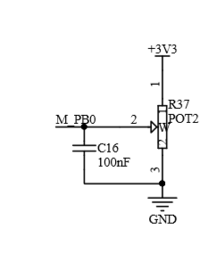
The use of ADC is the focus of the investigation. It has been observed in the provincial competitions, and the score accounts for a large proportion. Especially the ADC of the sliding resistance on board. Basic 100% examination
3.7.1 one way AD sampling
If the expansion board is not used, the AD sampling should be through the potentiometer R37 on the base board to adjust the voltage to capture and investigate the use of ADC
3.7.1.1 hardware connection of one channel AD sampling
3.7.1.2 software driver for multi-channel AD sampling (can also be used for one channel)
In the V3.5 library provided by the competition, under the folder "project - > stm32f10x ﹣ stdperiph ﹣ examples - > ADC - > ADC1 ﹣ DMA", open "main.c":
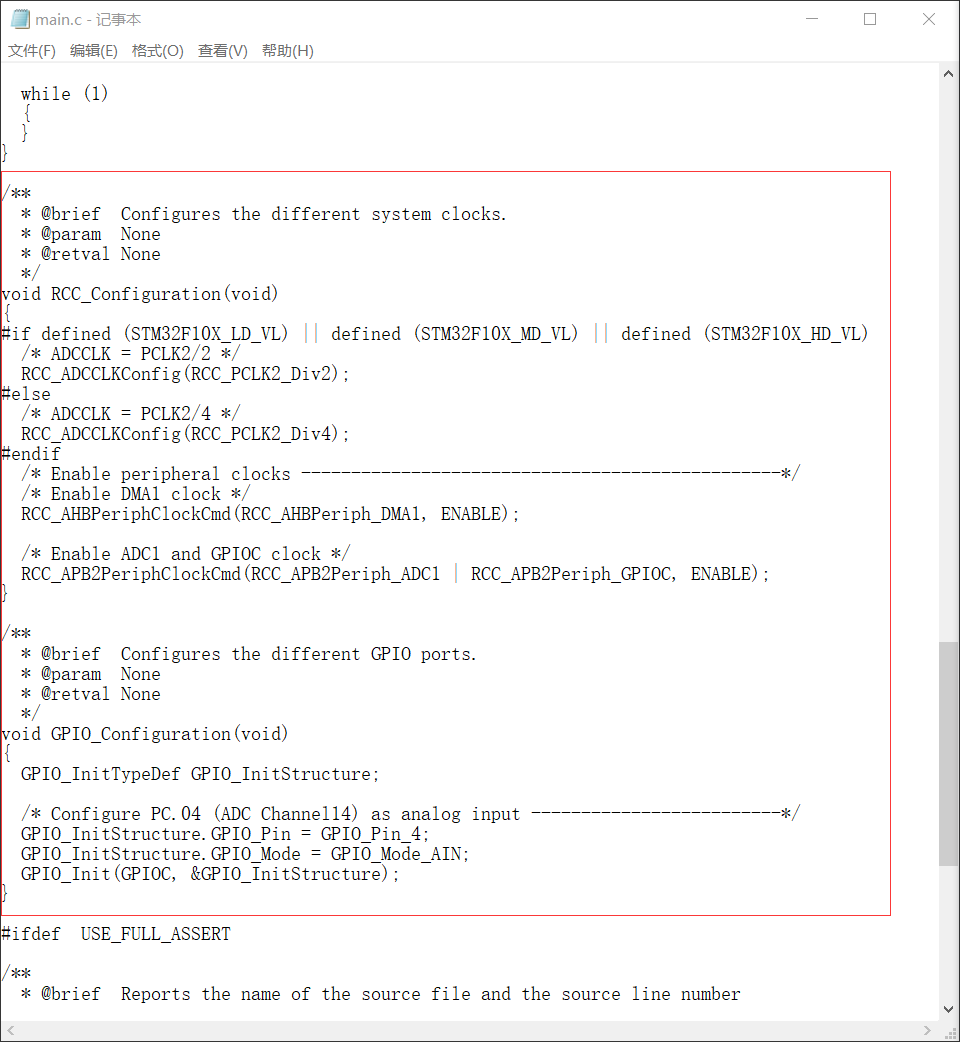
Because I don't need DMA to read values, I delete all the DMA related functions, and then I add RCC configuration functions to adc, which means adc is a function of adc
/************************************************************
***************************ADC*******************************
*************************************************************/
void RCC_Configuration_adc(void)
{
#if defined (STM32F10X_LD_VL) || defined (STM32F10X_MD_VL) || defined (STM32F10X_HD_VL)
/* ADCCLK = PCLK2/2 */
RCC_ADCCLKConfig(RCC_PCLK2_Div2);
#else
/* ADCCLK = PCLK2/4 */
RCC_ADCCLKConfig(RCC_PCLK2_Div4);
#endif
/* Enable ADC1 and GPIOC clock */
RCC_APB2PeriphClockCmd(RCC_APB2Periph_ADC1 | RCC_APB2Periph_GPIOA|RCC_APB2Periph_GPIOB, ENABLE);
}
/**
* @brief Configures the different GPIO ports.
* @param None
* @retval None
*/
void GPIO_Configuration_adc(void)
{
GPIO_InitTypeDef GPIO_InitStructure;
/* Configure PC.04 (ADC Channel14) as analog input -------------------------*/
GPIO_InitStructure.GPIO_Pin = GPIO_Pin_5;//I want to use io instead
GPIO_InitStructure.GPIO_Mode = GPIO_Mode_AIN;
GPIO_Init(GPIOA, &GPIO_InitStructure);
GPIO_InitStructure.GPIO_Pin = GPIO_Pin_0;//I want to use io instead
GPIO_Init(GPIOB, &GPIO_InitStructure);
}
#define ADC1_DR_Address ((uint32_t)0x4001244C)
void adc_init()
{
ADC_InitTypeDef ADC_InitStructure;
DMA_InitTypeDef DMA_InitStructure;
/* System clocks configuration ---------------------------------------------*/
RCC_Configuration_adc();
/* GPIO configuration ------------------------------------------------------*/
GPIO_Configuration_adc();
/* ADC1 configuration ------------------------------------------------------*/
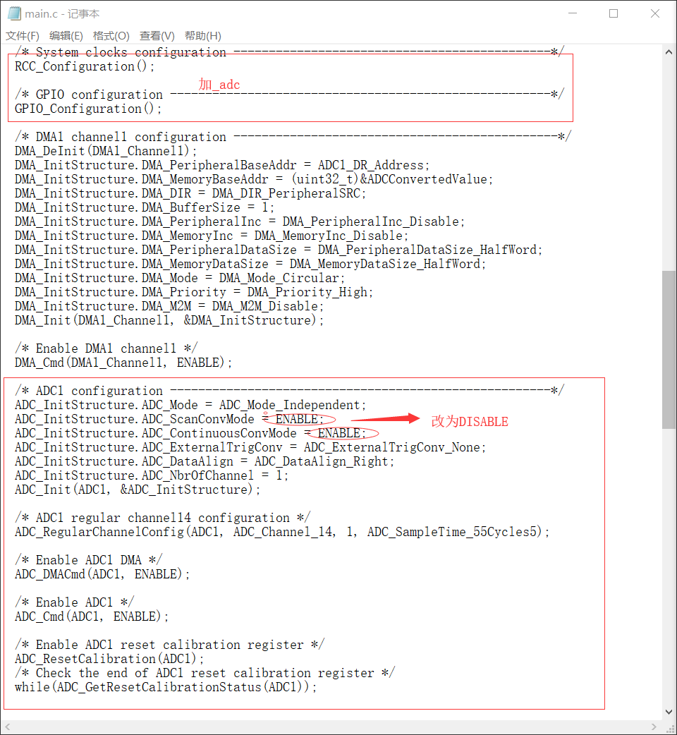
ADC_InitStructure.ADC_Mode = ADC_Mode_Independent;
ADC_InitStructure.ADC_ScanConvMode = DISABLE;//Changed
ADC_InitStructure.ADC_ContinuousConvMode = DISABLE;//Changed
ADC_InitStructure.ADC_ExternalTrigConv = ADC_ExternalTrigConv_None;
ADC_InitStructure.ADC_DataAlign = ADC_DataAlign_Right;
ADC_InitStructure.ADC_NbrOfChannel = 1;//It can be set from 1 to 16. The belt edge can be converted several ways at the same time, because we only convert one way at a time, so we don't change it.
ADC_Init(ADC1, &ADC_InitStructure);
/* Enable ADC1 */
ADC_Cmd(ADC1, ENABLE);//The above sentence is gone. The above sentence is to select the ADC channel to be acquired. Because we need to acquire different channels, we use it in the acquisition function
/* Enable ADC1 reset calibration register */
ADC_ResetCalibration(ADC1);
/* Check the end of ADC1 reset calibration register */
while(ADC_GetResetCalibrationStatus(ADC1));
/* Start ADC1 calibration */
ADC_StartCalibration(ADC1);
/* Check the end of ADC1 calibration */
while(ADC_GetCalibrationStatus(ADC1));
//Here, adc ﹣ softwarestartconvcmd (adc1, enable); I deleted it. This function is to enable adc conversion. We put it in the get function and set the channel to get once
}
u16 adc_data(u8 ch)//Add a new one. The first sentence is to select a channel (in initialization), and the second sentence starts to transform (in initialization),
//The third sentence is waiting for the end of the conversion. Remember that the official library file is in ADC.H, and the fourth sentence is in the 3acs? DMA interrupt function acquisition function
{
/* ADC1 regular channel14 configuration */
ADC_RegularChannelConfig(ADC1, ch, 1, ADC_SampleTime_55Cycles5);
/* Start ADC1 Software Conversion */
ADC_SoftwareStartConvCmd(ADC1, ENABLE);
while(!ADC_GetFlagStatus(ADC1,ADC_FLAG_EOC));
return ADC_GetConversionValue(ADC1);
}
After initialization, call adc_data to return the value collected by ADC. For example, if channel 8 is passed in, write 8
3.8PWM
PWM is the most important part. The goal of our training is
- Output PWM with adjustable duty cycle and frequency
- Capture the frequency and duty cycle of two PWM channels
Here must play very clear and skilled, PWM working principle I will not introduce, self-study
We should choose different ways to capture pwm or output pwm according to different topic requirements
3.8.1 capture the frequency of two-way PWM (I write two-way, one is simpler,)
In the V3.5 library provided by the competition, under the folder "project - > stm32f10x ﹣ stdperiph ﹣ examples - > tim - > inputcapture", the "main.c" and "stm32f10x it. C" respectively have the relevant codes of input capture mode initialization and interrupt service program: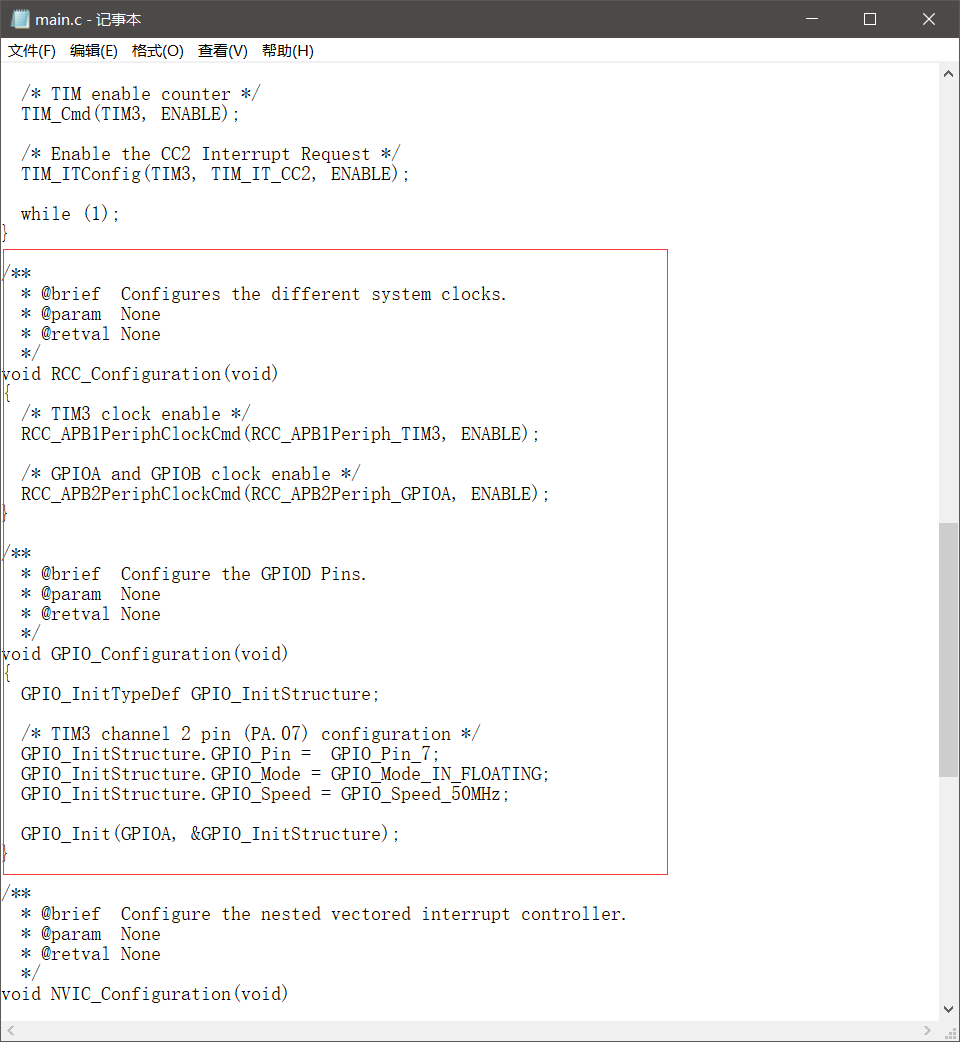
Variable location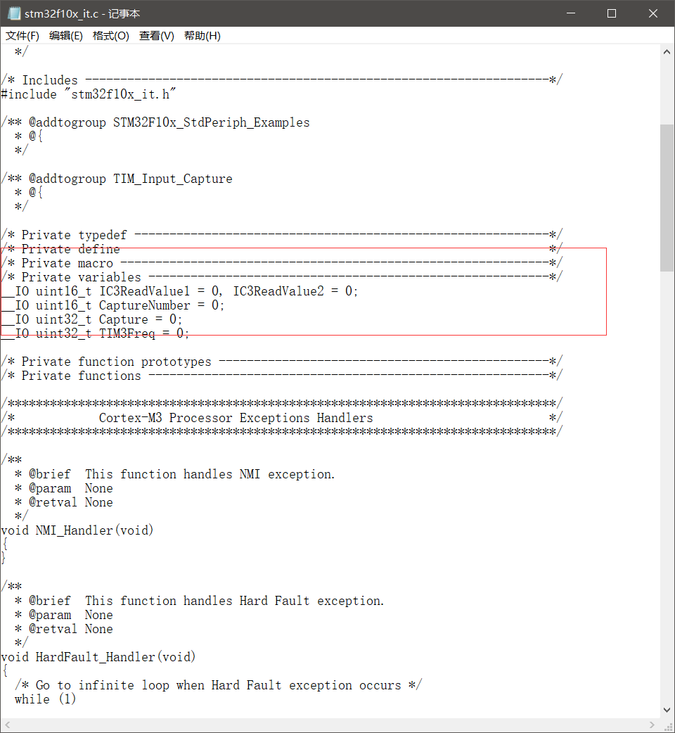
/*********************************************************************
************************Input capture*****************************************
******************************************************************/
//Refer to the InputCapture file, and remember to separate the interrupt read function
void RCC_Configuration_tim_input(void)
{
/* TIM2 clock enable */
RCC_APB1PeriphClockCmd(RCC_APB1Periph_TIM2, ENABLE);
/* GPIOA and GPIOB clock enable */
RCC_APB2PeriphClockCmd(RCC_APB2Periph_GPIOA, ENABLE);
}
/**
* @brief Configure the GPIOD Pins.
* @param None
* @retval None
*/
void GPIO_Configuration_tim_input(void)
{
GPIO_InitTypeDef GPIO_InitStructure;
/* TIM2 channel 2 pin (PA.07) configuration */
GPIO_InitStructure.GPIO_Pin = GPIO_Pin_1|GPIO_Pin_2;
GPIO_InitStructure.GPIO_Mode = GPIO_Mode_IN_FLOATING;
GPIO_InitStructure.GPIO_Speed = GPIO_Speed_50MHz;
GPIO_Init(GPIOA, &GPIO_InitStructure);
}
/**
* @brief Configure the nested vectored interrupt controller.
* @param None
* @retval None
*/
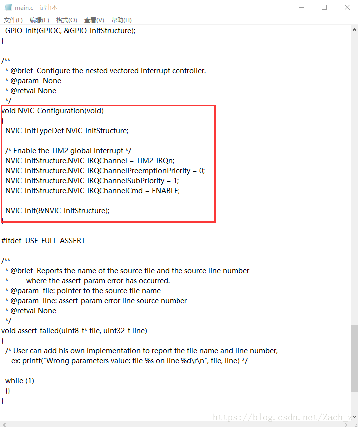
void NVIC_Configuration_tim_input(void)
{
NVIC_InitTypeDef NVIC_InitStructure;
/* Enable the TIM2 global Interrupt */
NVIC_InitStructure.NVIC_IRQChannel = TIM2_IRQn;
NVIC_InitStructure.NVIC_IRQChannelPreemptionPriority = 0;
NVIC_InitStructure.NVIC_IRQChannelSubPriority = 1;
NVIC_InitStructure.NVIC_IRQChannelCmd = ENABLE;
NVIC_Init(&NVIC_InitStructure);
}
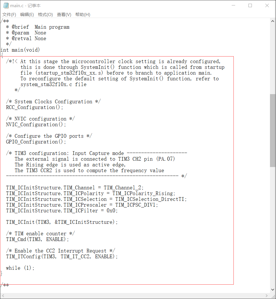
void tim_input_init()
{
TIM_ICInitTypeDef TIM_ICInitStructure;
/* System Clocks Configuration */
RCC_Configuration_tim_input();
/* NVIC configuration */
NVIC_Configuration_tim_input();
/* Configure the GPIO ports */
GPIO_Configuration_tim_input();
/* TIM2 configuration: Input Capture mode ---------------------
The external signal is connected to TIM2 CH2 pin (PA.07)
The Rising edge is used as active edge,
The TIM2 CCR2 is used to compute the frequency value
------------------------------------------------------------ */
TIM_ICInitStructure.TIM_Channel = TIM_Channel_2;
TIM_ICInitStructure.TIM_ICPolarity = TIM_ICPolarity_Rising;
TIM_ICInitStructure.TIM_ICSelection = TIM_ICSelection_DirectTI;
TIM_ICInitStructure.TIM_ICPrescaler = TIM_ICPSC_DIV1;
TIM_ICInitStructure.TIM_ICFilter = 0x0;
TIM_ICInit(TIM2, &TIM_ICInitStructure);
TIM_ICInitStructure.TIM_Channel = TIM_Channel_3;
TIM_ICInit(TIM2, &TIM_ICInitStructure);
/* TIM enable counter */
TIM_Cmd(TIM2, ENABLE);
/* Enable the CC2 Interrupt Request */
TIM_ITConfig(TIM2, TIM_IT_CC2|TIM_IT_CC3, ENABLE);
}
__IO uint16_t IC3ReadValue11 = 0, IC3ReadValue21 = 0;
__IO uint16_t CaptureNumber1 = 0;
__IO uint32_t Capture1 = 0;
__IO uint32_t TIM2Freq1 = 0;
__IO uint16_t IC3ReadValue12 = 0, IC3ReadValue22 = 0;
__IO uint16_t CaptureNumber2 = 0;
__IO uint32_t Capture2 = 0;
__IO uint32_t TIM2Freq2 = 0;
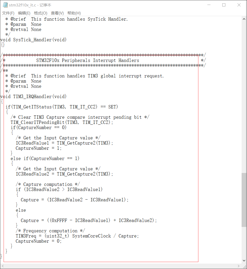
void TIM2_IRQHandler(void)
{
if(TIM_GetITStatus(TIM2, TIM_IT_CC2) == SET)
{
/* Clear TIM2 Capture compare interrupt pending bit */
TIM_ClearITPendingBit(TIM2, TIM_IT_CC2);
if(CaptureNumber1 == 0)
{
/* Get the Input Capture value */
IC3ReadValue11 = TIM_GetCapture2(TIM2);
CaptureNumber1 = 1;
}
else if(CaptureNumber1 == 1)
{
/* Get the Input Capture value */
IC3ReadValue21 = TIM_GetCapture2(TIM2);
/* Capture computation */
if (IC3ReadValue21 > IC3ReadValue11)
{
Capture1 = (IC3ReadValue21 - IC3ReadValue11);
}
else
{
Capture1 = ((0xFFFF - IC3ReadValue11) + IC3ReadValue21);
}
/* Frequency computation */
TIM2Freq1 = (uint32_t) SystemCoreClock / Capture1;
CaptureNumber1 = 0;
}
}
if(TIM_GetITStatus(TIM2, TIM_IT_CC3) == SET)
{
/* Clear TIM2 Capture compare interrupt pending bit */
TIM_ClearITPendingBit(TIM2, TIM_IT_CC3);
if(CaptureNumber2 == 0)
{
/* Get the Input Capture value */
IC3ReadValue12 = TIM_GetCapture3(TIM2);
CaptureNumber2 = 1;
}
else if(CaptureNumber2 == 1)
{
/* Get the Input Capture value */
IC3ReadValue22 = TIM_GetCapture3(TIM2);
/* Capture computation */
if (IC3ReadValue22 > IC3ReadValue12)
{
Capture2 = (IC3ReadValue22 - IC3ReadValue12);
}
else
{
Capture2 = ((0xFFFF - IC3ReadValue12) + IC3ReadValue22);
}
/* Frequency computation */
TIM2Freq2 = (uint32_t) SystemCoreClock / Capture2;
CaptureNumber2 = 0;
}
}
}
Call initialization, and then read TIM2Freq1 and TIM2Freq2 to input the capture value (frequency). It's good to directly delete the relevant code of the other way.
3.8.2 pwm with adjustable duty cycle and frequency
In the V3.5 library provided by the competition, under the folder "project - > stm32f10x ﹣ stdperiph ﹣ examples - > tim - > OCT toggle", open "main.c":
main function whole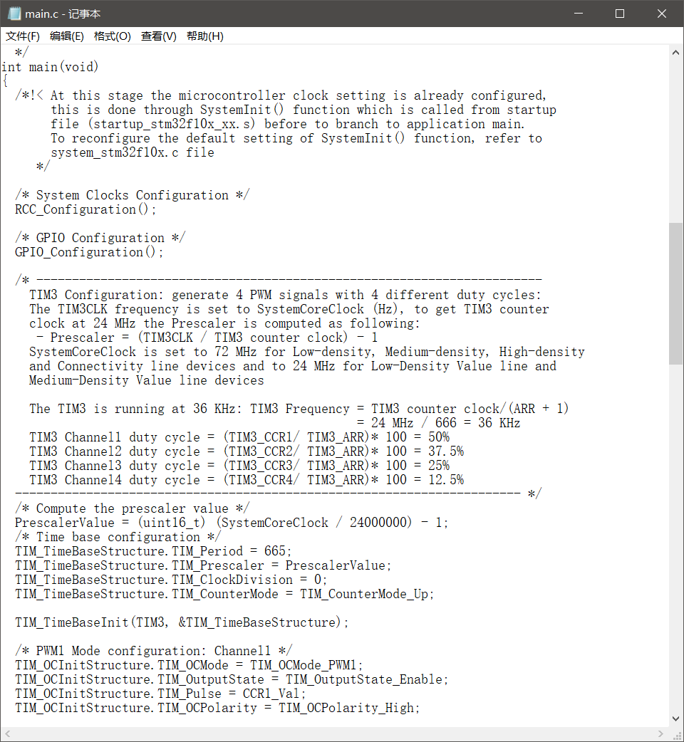
Location of variables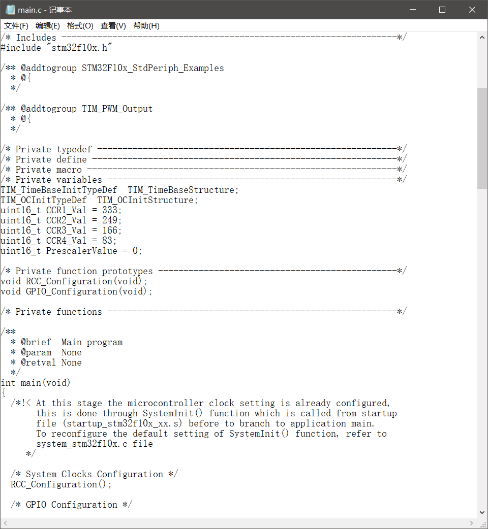
void RCC_Configuration_pwm(void)
{
  /* TIM3 clock enable */
  RCC_APB1PeriphClockCmd(RCC_APB1Periph_TIM3, ENABLE);

  /* GPIOA and GPIOB clock enable */
  RCC_APB2PeriphClockCmd(RCC_APB2Periph_GPIOA | RCC_APB2Periph_GPIOB |
                         RCC_APB2Periph_GPIOC | RCC_APB2Periph_AFIO, ENABLE);
}

/**
  * @brief  Configure the TIM3 Ouput Channels.
  * @param  None
  * @retval None
  */
void GPIO_Configuration_pwm(void)
{
  GPIO_InitTypeDef GPIO_InitStructure;

  /* GPIOA Configuration:TIM3 Channel1, 2, 3 and 4 as alternate function push-pull */
  GPIO_InitStructure.GPIO_Pin = GPIO_Pin_6 | GPIO_Pin_7;
  GPIO_InitStructure.GPIO_Mode = GPIO_Mode_AF_PP;
  GPIO_InitStructure.GPIO_Speed = GPIO_Speed_50MHz;

  GPIO_Init(GPIOA, &GPIO_InitStructure);
}


void NVIC_Configuration_pwm(void)
{
  NVIC_InitTypeDef NVIC_InitStructure;

  /* Enable the TIM3 global Interrupt */
  NVIC_InitStructure.NVIC_IRQChannel =  TIM3_IRQn;
  NVIC_InitStructure.NVIC_IRQChannelPreemptionPriority = 2;
  NVIC_InitStructure.NVIC_IRQChannelSubPriority = 2;
  NVIC_InitStructure.NVIC_IRQChannelCmd = ENABLE;
  NVIC_Init(&NVIC_InitStructure);
}

void pwm_out_init()
{
    TIM_TimeBaseInitTypeDef  TIM_TimeBaseStructure;
    TIM_OCInitTypeDef  TIM_OCInitStructure;
    uint16_t CCR1Val = 333;
    uint16_t CCR2Val = 249;
    uint16_t PrescalerValue = 0;
      /*!< At this stage the microcontroller clock setting is already configured,
       this is done through SystemInit() function which is called from startup
       file (startup_stm32f10x_xx.s) before to branch to application main.
       To reconfigure the default setting of SystemInit() function, refer to
       system_stm32f10x.c file
     */

  /* System Clocks Configuration */
  RCC_Configuration_pwm();

  /* GPIO Configuration */
  GPIO_Configuration_pwm();

  /* NVIC Configuration */
  NVIC_Configuration_pwm();

  /* -----------------------------------------------------------------------
    TIM3 Configuration: generate 4 PWM signals with 4 different duty cycles:
    The TIM3CLK frequency is set to SystemCoreClock (Hz), to get TIM3 counter
    clock at 24 MHz the Prescaler is computed as following:
     - Prescaler = (TIM3CLK / TIM3 counter clock) - 1
    SystemCoreClock is set to 72 MHz for Low-density, Medium-density, High-density
    and Connectivity line devices and to 24 MHz for Low-Density Value line and
    Medium-Density Value line devices

    The TIM3 is running at 36 KHz: TIM3 Frequency = TIM3 counter clock/(ARR + 1)
                                                  = 24 MHz / 666 = 36 KHz
    TIM3 Channel1 duty cycle = (TIM3_CCR1/ TIM3_ARR)* 100 = 50%
    TIM3 Channel2 duty cycle = (TIM3_CCR2/ TIM3_ARR)* 100 = 37.5%
    TIM3 Channel3 duty cycle = (TIM3_CCR3/ TIM3_ARR)* 100 = 25%
    TIM3 Channel4 duty cycle = (TIM3_CCR4/ TIM3_ARR)* 100 = 12.5%
  ----------------------------------------------------------------------- */
  /* Compute the prescaler value */
  PrescalerValue = (uint16_t) (SystemCoreClock / 24000000) - 1;

  /* Time base configuration */
  TIM_TimeBaseStructure.TIM_Period = 65535;
  TIM_TimeBaseStructure.TIM_Prescaler = PrescalerValue;
  TIM_TimeBaseStructure.TIM_ClockDivision = 0;
  TIM_TimeBaseStructure.TIM_CounterMode = TIM_CounterMode_Up;

  TIM_TimeBaseInit(TIM3, &TIM_TimeBaseStructure);

  /* Output Compare Toggle Mode configuration: Channel1 */
  TIM_OCInitStructure.TIM_OCMode = TIM_OCMode_Toggle;
  TIM_OCInitStructure.TIM_OutputState = TIM_OutputState_Enable;
  TIM_OCInitStructure.TIM_Pulse = CCR1Val;
  TIM_OCInitStructure.TIM_OCPolarity = TIM_OCPolarity_Low;
  TIM_OC1Init(TIM3, &TIM_OCInitStructure);

  TIM_OC1PreloadConfig(TIM3, TIM_OCPreload_Disable);

  /* Output Compare Toggle Mode configuration: Channel2 */
  TIM_OCInitStructure.TIM_OutputState = TIM_OutputState_Enable;
  TIM_OCInitStructure.TIM_Pulse = CCR2Val;

  TIM_OC2Init(TIM3, &TIM_OCInitStructure);

  TIM_OC2PreloadConfig(TIM3, TIM_OCPreload_Disable);

  /* TIM enable counter */
  TIM_Cmd(TIM3, ENABLE);

  /* TIM IT enable */
  TIM_ITConfig(TIM3, TIM_IT_CC1 | TIM_IT_CC2, ENABLE);

}
There are interrupt service functions in stm32f10x it. C under the same directory
uint16_t capture = 0;
__IO uint16_t CCR1Val;//You can change the frequency by changing this value
__IO uint16_t CCR2Val;
void TIM3_IRQHandler(void)
{
  /* TIM3_CH1 toggling with frequency = 366.2 Hz */
  if (TIM_GetITStatus(TIM3, TIM_IT_CC1) != RESET)
  {
    TIM_ClearITPendingBit(TIM3, TIM_IT_CC1 );
    capture = TIM_GetCapture1(TIM3);
    TIM_SetCompare1(TIM3, capture + CCR1Val );
  }

  /* TIM3_CH2 toggling with frequency = 732.4 Hz */
  if (TIM_GetITStatus(TIM3, TIM_IT_CC2) != RESET)
  {
    TIM_ClearITPendingBit(TIM3, TIM_IT_CC2);
    capture = TIM_GetCapture2(TIM3);
    TIM_SetCompare2(TIM3, capture + CCR2Val);
  }
}
At the same time, Tim? Setcompare1 (tim312000); is to change the duty cycle.
3.8.3PWM output frequency fixed change duty cycle
In the V3.5 library provided by the competition, open "main.c" under the folder "project - > stm32f10x" ﹣ stdperiph ﹣ examples - > tim - > PWM ﹣ output ":
Copy all main functions, and then remove while
Variable definition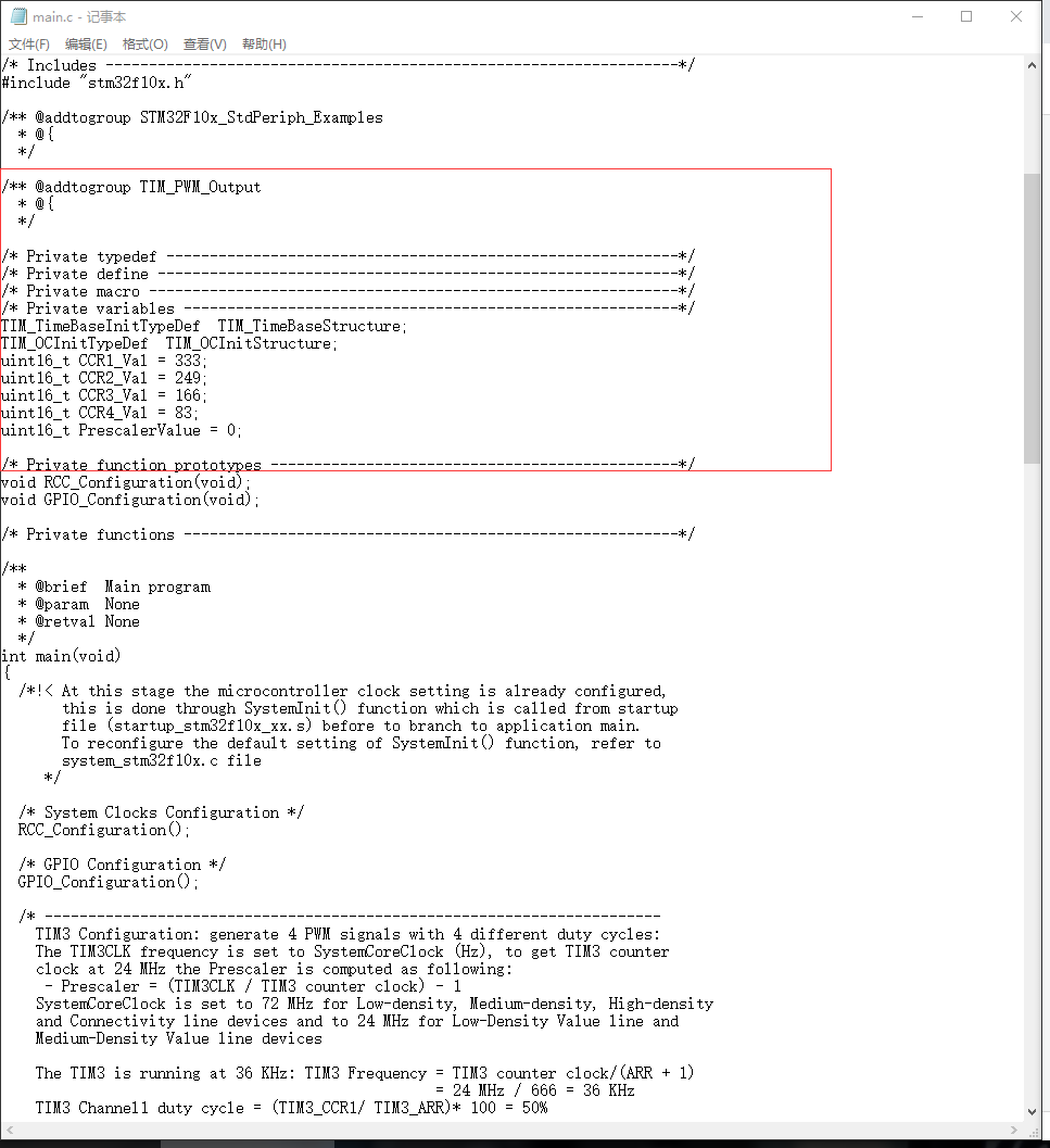
io port initialization
void RCC_Configuration_pwm(void)
{
  /* TIM3 clock enable */
  RCC_APB1PeriphClockCmd(RCC_APB1Periph_TIM3, ENABLE);

  /* GPIOA and GPIOB clock enable */
  RCC_APB2PeriphClockCmd(RCC_APB2Periph_GPIOA | RCC_APB2Periph_GPIOB |RCC_APB2Periph_AFIO, ENABLE);
}

/**
  * @brief  Configure the TIM3 Ouput Channels.
  * @param  None
  * @retval None
  */
void GPIO_Configuration_pwm(void)
{
  GPIO_InitTypeDef GPIO_InitStructure;

  /* GPIOA Configuration:TIM3 Channel1, 2, 3 and 4 as alternate function push-pull */
  GPIO_InitStructure.GPIO_Pin = GPIO_Pin_6 | GPIO_Pin_7;
  GPIO_InitStructure.GPIO_Mode = GPIO_Mode_AF_PP;
  GPIO_InitStructure.GPIO_Speed = GPIO_Speed_50MHz;

  GPIO_Init(GPIOA, &GPIO_InitStructure);

  GPIO_InitStructure.GPIO_Pin = GPIO_Pin_0 | GPIO_Pin_1;
  GPIO_Init(GPIOB, &GPIO_InitStructure);

}

void pwm_out_init()
{
    TIM_TimeBaseInitTypeDef  TIM_TimeBaseStructure;
    TIM_OCInitTypeDef  TIM_OCInitStructure;
    uint16_t CCR1_Val = 333;
    uint16_t CCR2_Val = 249;
    uint16_t CCR3_Val = 166;
    uint16_t CCR4_Val = 83;
    uint16_t PrescalerValue = 0;
     /*!< At this stage the microcontroller clock setting is already configured,
       this is done through SystemInit() function which is called from startup
       file (startup_stm32f10x_xx.s) before to branch to application main.
       To reconfigure the default setting of SystemInit() function, refer to
       system_stm32f10x.c file
     */

  /* System Clocks Configuration */
  RCC_Configuration_pwm();

  /* GPIO Configuration */
  GPIO_Configuration_pwm();

  /* -----------------------------------------------------------------------
    TIM3 Configuration: generate 4 PWM signals with 4 different duty cycles:
    The TIM3CLK frequency is set to SystemCoreClock (Hz), to get TIM3 counter
    clock at 24 MHz the Prescaler is computed as following:
     - Prescaler = (TIM3CLK / TIM3 counter clock) - 1
    SystemCoreClock is set to 72 MHz for Low-density, Medium-density, High-density
    and Connectivity line devices and to 24 MHz for Low-Density Value line and
    Medium-Density Value line devices

    The TIM3 is running at 1 KHz: TIM3 Frequency = TIM3 counter clock/(ARR + 1)
                                                  = 24 MHz / 24k = 1 KHz
    TIM3 Channel1 duty cycle = (TIM3_CCR1/ TIM3_ARR)* 100 = 50%
    TIM3 Channel2 duty cycle = (TIM3_CCR2/ TIM3_ARR)* 100 = 37.5%
    TIM3 Channel3 duty cycle = (TIM3_CCR3/ TIM3_ARR)* 100 = 25%
    TIM3 Channel4 duty cycle = (TIM3_CCR4/ TIM3_ARR)* 100 = 12.5%
  ----------------------------------------------------------------------- */
  /* Compute the prescaler value */
  PrescalerValue = (uint16_t) (SystemCoreClock / 24000000) - 1;//Set the counting speed, current 24000000hz,
  /* Time base configuration */
  TIM_TimeBaseStructure.TIM_Period = 24000-1;//Set the reload value. Add it to the value and then reload
  TIM_TimeBaseStructure.TIM_Prescaler = PrescalerValue;
  TIM_TimeBaseStructure.TIM_ClockDivision = 0;
  TIM_TimeBaseStructure.TIM_CounterMode = TIM_CounterMode_Up;

  TIM_TimeBaseInit(TIM3, &TIM_TimeBaseStructure);

  /* PWM1 Mode configuration: Channel1 */
  TIM_OCInitStructure.TIM_OCMode = TIM_OCMode_PWM1;
  TIM_OCInitStructure.TIM_OutputState = TIM_OutputState_Enable;
  TIM_OCInitStructure.TIM_Pulse = CCR1_Val;//Set flip value
  TIM_OCInitStructure.TIM_OCPolarity = TIM_OCPolarity_High;

  TIM_OC1Init(TIM3, &TIM_OCInitStructure);

  TIM_OC1PreloadConfig(TIM3, TIM_OCPreload_Enable);//Initialize tim-cc1

  /* PWM1 Mode configuration: Channel2 */
  TIM_OCInitStructure.TIM_OutputState = TIM_OutputState_Enable;
  TIM_OCInitStructure.TIM_Pulse = CCR2_Val;

  TIM_OC2Init(TIM3, &TIM_OCInitStructure);//Initialize tim-cc2

  TIM_OC2PreloadConfig(TIM3, TIM_OCPreload_Enable);

  /* PWM1 Mode configuration: Channel3 */
  TIM_OCInitStructure.TIM_OutputState = TIM_OutputState_Enable;
  TIM_OCInitStructure.TIM_Pulse = CCR3_Val;

  TIM_OC3Init(TIM3, &TIM_OCInitStructure);

  TIM_OC3PreloadConfig(TIM3, TIM_OCPreload_Enable);

  /* PWM1 Mode configuration: Channel4 */
  TIM_OCInitStructure.TIM_OutputState = TIM_OutputState_Enable;
  TIM_OCInitStructure.TIM_Pulse = CCR4_Val;

  TIM_OC4Init(TIM3, &TIM_OCInitStructure);

  TIM_OC4PreloadConfig(TIM3, TIM_OCPreload_Enable);

  TIM_ARRPreloadConfig(TIM3, ENABLE);

  /* TIM3 enable counter */
  TIM_Cmd(TIM3, ENABLE);
}
- It can be seen that the counting frequency of TIM2 is 24m and the reload value is 24k. It is proved that our frequency is 24Mhz/24k=1Khz
- We directly set CH1 and CH2, CH3 and CH4 of TIM3 to PWM output mode 1, and the output polarity is high
- Change the duty cycle function tim_setcompare1 (tim312000); change the previous 1 to 2 to modify CH2, and the later value is the duty cycle. The specific duty cycle needs to use the value you set to remove the reload value and multiply by 100%, such as my 12000 / 24000 * 100% = 50%.
Here, we can change the duty cycle after initialization. If we only need one way, we can delete the related functions and variables of other ways
3.8.4 capture the frequency and duty cycle of one PWM circuit
In the V3.5 library provided by the competition, under the folder of "project - > stm32f10 ﹣ stdperiph ﹣ examples - > tim - > PWM ﹣ input", the "main.c" and "stm32f10x it. C" respectively have the relevant codes of PWM input mode initialization and interrupt service program: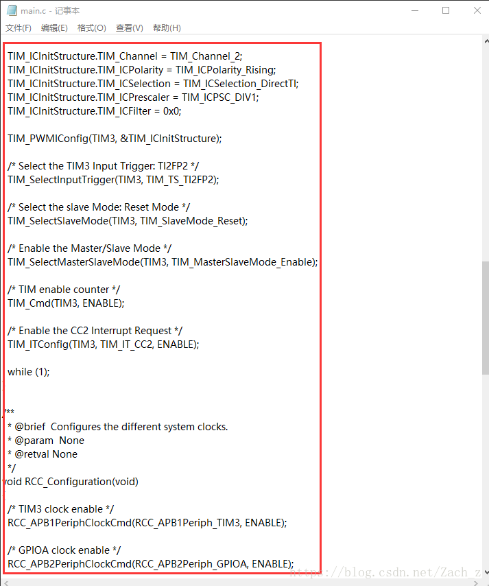
Just change to the pin you need and the corresponding clock channel
void capture_Init()
{
TIM_ICInitTypeDef TIM_ICInitStructure;
GPIO_InitTypeDef GPIO_InitStructure;
NVIC_InitTypeDef NVIC_InitStructure;
RCC_APB1PeriphClockCmd(RCC_APB1Periph_TIM3, ENABLE);
RCC_APB2PeriphClockCmd(RCC_APB2Periph_GPIOA, ENABLE);
GPIO_InitStructure.GPIO_Pin = GPIO_Pin_6;
GPIO_InitStructure.GPIO_Mode = GPIO_Mode_IN_FLOATING;
GPIO_InitStructure.GPIO_Speed = GPIO_Speed_50MHz;
GPIO_Init(GPIOA, &GPIO_InitStructure);
NVIC_InitStructure.NVIC_IRQChannel = TIM3_IRQn;
NVIC_InitStructure.NVIC_IRQChannelPreemptionPriority = 0;
NVIC_InitStructure.NVIC_IRQChannelSubPriority = 1;
NVIC_InitStructure.NVIC_IRQChannelCmd = ENABLE;
NVIC_Init(&NVIC_InitStructure);
TIM_ICInitStructure.TIM_Channel = TIM_Channel_1;
TIM_ICInitStructure.TIM_ICPolarity = TIM_ICPolarity_Rising;
TIM_ICInitStructure.TIM_ICSelection = TIM_ICSelection_DirectTI;
TIM_ICInitStructure.TIM_ICPrescaler = TIM_ICPSC_DIV1;
TIM_ICInitStructure.TIM_ICFilter = 0x0;
TIM_PWMIConfig(TIM3, &TIM_ICInitStructure);
TIM_SelectInputTrigger(TIM3, TIM_TS_TI1FP1);
TIM_SelectSlaveMode(TIM3, TIM_SlaveMode_Reset);
TIM_SelectMasterSlaveMode(TIM3, TIM_MasterSlaveMode_Enable);
TIM_Cmd(TIM3, ENABLE);
TIM_ITConfig(TIM3, TIM_IT_CC1, ENABLE);
}
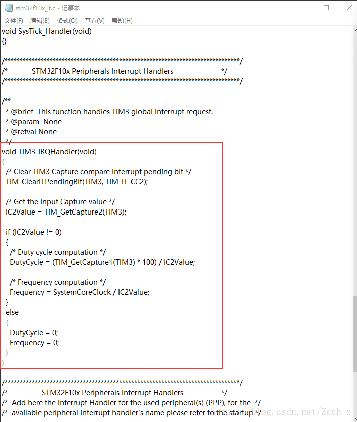
__IO uint16_t IC2Value = 0;
__IO uint16_t DutyCycle = 0;
__IO uint32_t Frequency = 0;
void TIM3_IRQHandler(void)
{
TIM_ClearITPendingBit(TIM3, TIM_IT_CC1);
IC2Value = TIM_GetCapture1(TIM3);
if (IC2Value != 0)
{
DutyCycle = (TIM_GetCapture2 (TIM3) * 100) / IC2Value;
Frequency = SystemCoreClock / IC2Value;
}
else
{
DutyCycle = 0;
Frequency = 0;
}
}
- DutyCycle is the duty cycle
- Frequency is frequency
- You can divide the clock frequency, but when you calculate the frequency, you need to divide it by the number of frequency divisions
3.9 matrix button of expansion board
The 8 buttons of the expansion board determine which button is based on the voltage sampled by AD to the corresponding pin
The ADC driver has talked about how to write, so skip the ADC part
The expansion key connects PA5 to AKEY through jumper cap
The 8 keys should be noted:
- As like as two peas on the principle board, the resistance on the plate is biased, because no two element parameters are exactly the same in the world, so the test is started directly, starting with a button test from small to large.
- It will take less than 10 minutes to try out 8 keys. This is my solution
Directly paste out the button driver of the expansion version:
void adc_key_Init()
{
    ADC_InitTypeDef ADC_InitStructure;

	GPIO_InitTypeDef GPIO_InitStructure;

	RCC_APB2PeriphClockCmd(RCC_APB2Periph_ADC1 | RCC_APB2Periph_GPIOA, ENABLE);


    GPIO_InitStructure.GPIO_Pin = GPIO_Pin_5;
    GPIO_InitStructure.GPIO_Mode = GPIO_Mode_AIN;
    GPIO_Init(GPIOA, &GPIO_InitStructure);

    ADC_InitStructure.ADC_Mode = ADC_Mode_Independent;
    ADC_InitStructure.ADC_ScanConvMode = DISABLE;
    ADC_InitStructure.ADC_ContinuousConvMode = DISABLE;
    ADC_InitStructure.ADC_ExternalTrigConv = ADC_ExternalTrigConv_None;
    ADC_InitStructure.ADC_DataAlign = ADC_DataAlign_Right;
    ADC_InitStructure.ADC_NbrOfChannel = 1;
    ADC_Init(ADC1, &ADC_InitStructure);

    ADC_RegularChannelConfig(ADC1, ADC_Channel_5, 1, ADC_SampleTime_55Cycles5);

    ADC_Cmd(ADC1, ENABLE);
    ADC_ResetCalibration(ADC1);
    while(ADC_GetResetCalibrationStatus(ADC1));
    ADC_StartCalibration(ADC1);
    while(ADC_GetCalibrationStatus(ADC1));
}

u8 get_button()
{
	u16 btn_tmp;
	ADC_SoftwareStartConvCmd(ADC1, ENABLE);//Start ADC conversion
	while(!ADC_GetFlagStatus( ADC1,  ADC_FLAG_EOC));//Wait for ADC conversion to finish
	btn_tmp=ADC_GetConversionValue(ADC1);//Get adc value

	if(btn_tmp <= 0x0020)//Write the range of values for each key press
	{
		return 1;
	}
	else if((btn_tmp >= 0x00B0) && (btn_tmp <= 0x0100))
	{
		return 2;
	}
	else if((btn_tmp >= 0x0240) && (btn_tmp <= 0x0300))
	{
		return 3;
	}
	else if((btn_tmp >= 0x03B0) && (btn_tmp <= 0x0450))
	{
		return 4;
	}
	else if((btn_tmp >= 0x0450) && (btn_tmp <= 0x0700))
	{
		return 5;
	}
	else if((btn_tmp >= 0x0700) && (btn_tmp <= 0x0800))
	{
		return 6;
	}
	else if((btn_tmp >= 0x0840) && (btn_tmp <= 0x0940))
	{
		return 7;
	}
	else if(btn_tmp <= 0x0B50)
	{
		return 8;
	}
	else
	{
		return 0;	//error status & no key
	}
}
3.10 nixie tube on the expansion board
3.10.1 hardware connection of nixie tube
First of all, don't say I won't use it. I used it when I was competing in China. It let me use a digital tube to display the temperature. At the same time, I need to use USART 2 to send data. However, the pins of these two modules are just in conflict. They both use PA2 and PA3, so what I wrote at that time was exciting.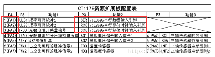
- PA1~3 can be connected to the corresponding pin on P3 with jumper cap
3.10.2 software driver of nixie tube
- Here, I need to be familiar with the segment code of the nixie tube. I was quite familiar with it at that time. Then I wrote the segment display array while testing. It can be done in 2 minutes.
- Here, the communication mode of 74hc595 is serial to parallel, that is, the time signal (pin 11 of 595) controls the serial port data to go through the serial port data input io of 595 (pin 14 of 595) to input one bit by one. We have three 595 on board, so we need to input 24 bits of data in total. And the 595 is written first to the high bit, that is, the first bit is written to QH, and the last bit is written to QA. (when the first 595 is written to 8 bits and is not updated, the data will be written again, and the overall data of 595 will move one bit backward, and the starting highest bit data will go to QH and output to the next 595.)
- The data update pin of 595 is 12 pins. When the rising edge is reached, the data acquired by the serial port is output to the parallel port.
#define SER_H GPIO_SetBits(GPIOA,GPIO_Pin_1)
#define SER_L GPIO_ResetBits(GPIOA,GPIO_Pin_1)

#define RCK_H GPIO_SetBits(GPIOA,GPIO_Pin_2)
#define RCK_L GPIO_ResetBits(GPIOA,GPIO_Pin_2)

#define SCK_H GPIO_SetBits(GPIOA,GPIO_Pin_3)
#define SCK_L GPIO_ResetBits(GPIOA,GPIO_Pin_3)


u8 seg[17]={ 0x3f,0x06,0x5b,0x4f,0x66,0x6d,0x7d,0x07,0x7f,0x6f,0x77,0x7c,0x39,0x5e,0x79,0x71,0x00}; //Remember to be familiar with it, otherwise it will take time to spell one by one
void seg_Init()//Initialize to push pull output
{
	GPIO_InitTypeDef GPIO_InitStructure;

	RCC_APB2PeriphClockCmd(RCC_APB2Periph_GPIOA, ENABLE);

	GPIO_InitStructure.GPIO_Pin = GPIO_Pin_1|GPIO_Pin_2|GPIO_Pin_3;
  GPIO_InitStructure.GPIO_Speed = GPIO_Speed_50MHz;
  GPIO_InitStructure.GPIO_Mode = GPIO_Mode_Out_PP;
  GPIO_Init(GPIOA, &GPIO_InitStructure);

	GPIO_ResetBits(GPIOA,GPIO_Pin_1);
	GPIO_ResetBits(GPIOA,GPIO_Pin_2);
	GPIO_ResetBits(GPIOA,GPIO_Pin_3);
}

void seg_Control(u8 bit1, u8 bit2, u8 bit3)
{
	u8 temp,i;

	temp=seg[bit3];
	for(i=0;i<8;i++)
	{
		if(temp&0x80)SER_H;
		else SER_L;

		temp=temp<<1;
		SCK_L;
		delay_ms(1);
		SCK_H;
	}

	temp=seg[bit2];
	for(i=0;i<8;i++)
	{
		if(temp&0x80)SER_H;
		else SER_L;

		temp=temp<<1;
		SCK_L;
		delay_ms(1);
		SCK_H;
	}

	temp=seg[bit1];
	for(i=0;i<8;i++)
	{
		if(temp&0x80)SER_H;
		else SER_L;

		temp=temp<<1;
		SCK_L;
		delay_ms(1);
		SCK_H;
	}

	RCK_L;//Data updating
	delay_ms(1);
	RCK_H;
}
Call the function SEG UU control(); just pass in the value to be displayed, such as SEG UU control (1,2,3); the display is 123.
3.11 use of DS18B20 driver
ds18b20 is a temperature sensor
Because the game provides ds18b20 driver files, so directly add. c and. h files to our HARDWARE folder, and add them to the project.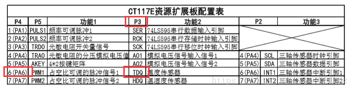
Here we need to pay attention to the fact that the game does not give the reading function, and we need to write by ourselves, that is, I have no part of the circle below. There is no good way to solve this problem by reciting it. I was lucky. I just remember the time sequence. Otherwise, I would play myself to death.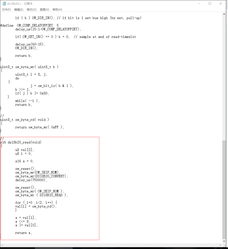
I don't suggest you take the time to read the data book here. It's too much time.
The most important thing here is data splicing. It is important to remember that the first eight bits read out are the high ones. Then the read value needs to be multiplied by 0.625 to get the temperature value.
int ds18b20_read(void)
{
   uint8_t val[2];
   uint8_t i = 0;

	int x = 0;

  	ow_reset();
  	ow_byte_wr(OW_SKIP_ROM);
  	ow_byte_wr(DS18B20_CONVERT);
  	delay_us(750000);

  	ow_reset();
  	ow_byte_wr( OW_SKIP_ROM );
  	ow_byte_wr ( DS18B20_READ );

  	for ( i=0 ;i<2; i++) {
    	val[i] = ow_byte_rd();
  	}

  	x = val[1];
	x <<= 8;
	x |= val[0];

	x=(float)x*0.0625*10;//To enlarge the temperature by ten times is equivalent to keeping one decimal place
	return x;
}
3.12 use of DHT11
DHT11 is a temperature and humidity sensor
Because the game provides dht11 driver files, so directly add. c and. h files to our HARDWARE folder, and add them to the project.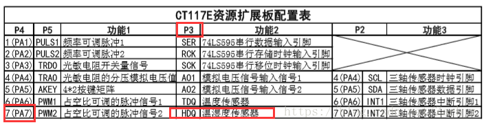
PA7 can drive dht11 temperature and humidity sensor by connecting the jumper cap with the corresponding pin on P3
Again, I guess it won't provide the code to read,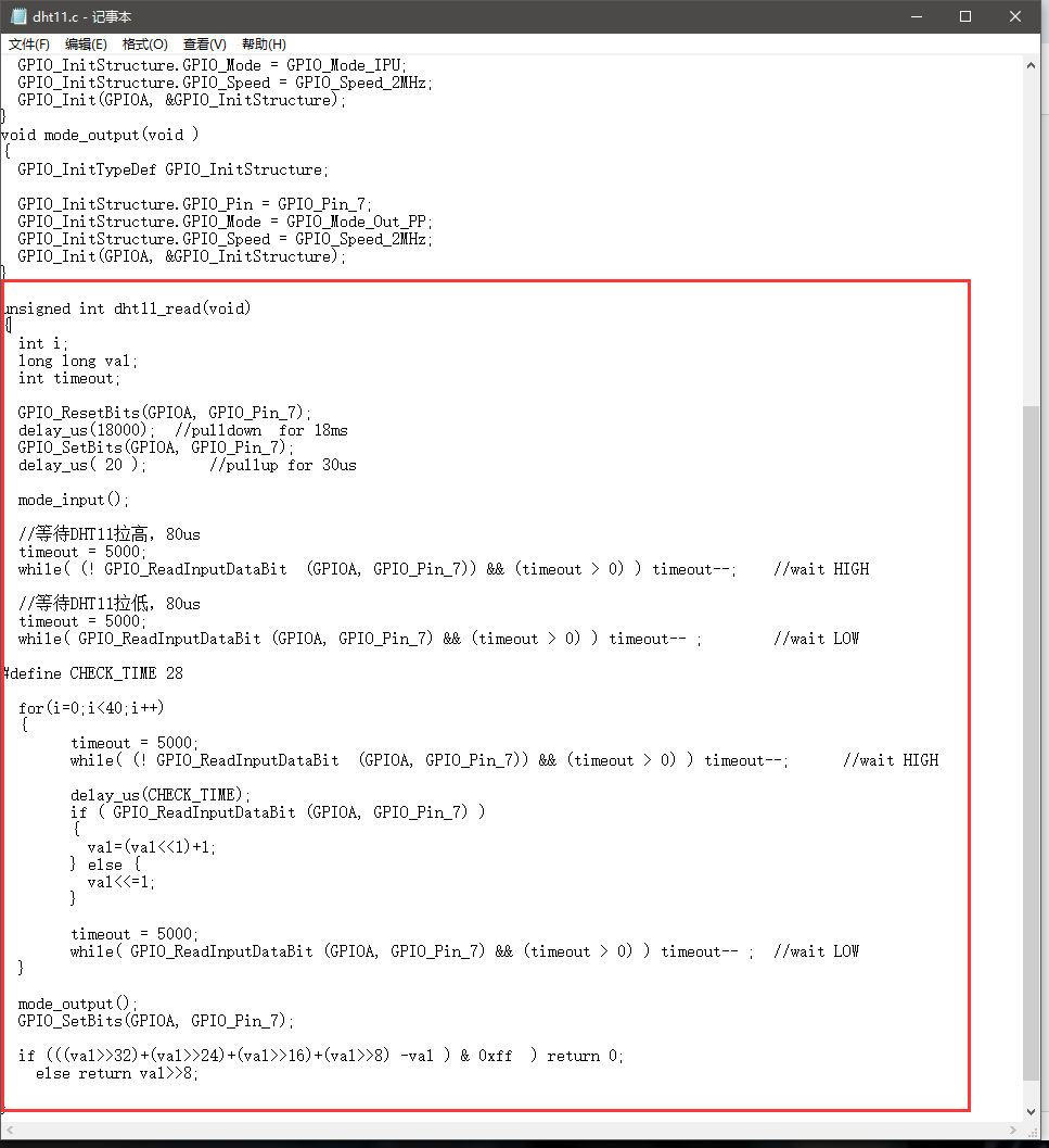
So, remember this code
unsigned int dht11_read(void)
{
  int i;
  long long val;
  int timeout;

  GPIO_ResetBits(GPIOA, GPIO_Pin_7);
  delay_us(18000);  //pulldown  for 18ms
  GPIO_SetBits(GPIOA, GPIO_Pin_7);
  delay_us( 20 );	//pullup for 30us

  mode_input();

  //Wait for DHT11 to pull up, 80us
  timeout = 5000;
  while( (! GPIO_ReadInputDataBit  (GPIOA, GPIO_Pin_7)) && (timeout > 0) ) timeout--;	 //wait HIGH

  //Wait for DHT11 to pull down, 80us
  timeout = 5000;
  while( GPIO_ReadInputDataBit (GPIOA, GPIO_Pin_7) && (timeout > 0) ) timeout-- ;	 //wait LOW

#define CHECK_TIME 28

  for(i=0;i<40;i++)
  {
	timeout = 5000;
	while( (! GPIO_ReadInputDataBit  (GPIOA, GPIO_Pin_7)) && (timeout > 0) ) timeout--;	 //wait HIGH

	delay_us(CHECK_TIME);
	if ( GPIO_ReadInputDataBit (GPIOA, GPIO_Pin_7) )
	{
	  val=(val<<1)+1;
	} else {
	  val<<=1;
	}

	timeout = 5000;
	while( GPIO_ReadInputDataBit (GPIOA, GPIO_Pin_7) && (timeout > 0) ) timeout-- ;	 //wait LOW
  }

  mode_output();
  GPIO_SetBits(GPIOA, GPIO_Pin_7);

  if (((val>>32)+(val>>24)+(val>>16)+(val>>8) -val ) & 0xff  ) return 0;
    else return val>>8;
}

/***********************************************
*****************DHT11***************************
************************************************/
//Read out the value must be written like this!!! Otherwise it's not worth it.
        dht11_value=dht11_read();
        Delay_Ms(10);
        if(dht11_value!=0)
        {
            sprintf(temp,"%s%2d%%"," shidu:",dht11_value>>24);//Humidity value = DHT11 < value > > 24
            LCD_DisplayStringLine(Line4 ,temp);
            sprintf(temp,"%s%2d","  wendu:",(dht11_value>>8)&0XFF);//Temperature value = (dht11_value > > 8) & 0xff
            LCD_DisplayStringLine(Line6 ,temp);
        }
3.13 triaxial sensor
Generally, this thing will not be inspected, just like the buzzer, it will be a mess in the inspection room. This thing also needs to turn around with the board, and it takes up a lot of pins. However, there is no need to inspect the expansion board in recent years, so there will be a three-axis sensor problem. It's better to master how to write the drive.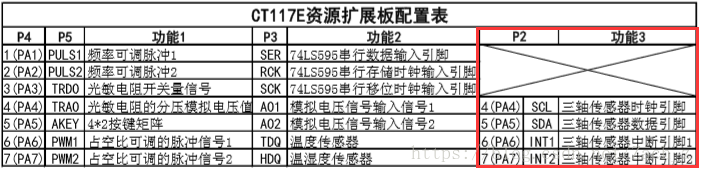
- PA4~7 can't be used for other purposes. Three week sensors need to use these four pin resources
- P2 all short circuited
The communication protocol of this peripheral is the same as that of E2PROM, so we are familiar with it.
It mainly includes the following two points: - Change SDA and SCL pins in I2C driver
- Correctly configure the three-axis sensor
/** I2C Bus interface */
#define I2C_PORT GPIOA
#define SDA_Pin	GPIO_Pin_5
#define SCL_Pin GPIO_Pin_4

u8 alz[3] ;

//Writing data
void LIS302DL_Write(unsigned char reg,unsigned char info)
{
	I2CStart();
	I2CSendByte(0x38);
	I2CWaitAck();
	I2CSendByte(reg);
	I2CWaitAck();
	I2CSendByte(info);
	I2CWaitAck();
	I2CStop();
}

//Read data
uint8_t LIS302DL_Read(uint8_t address)
{
	unsigned char val;
	I2CStart();
	I2CSendByte(0x38);
	I2CWaitAck();

	I2CSendByte(address);
	I2CWaitAck();

	I2CStart();
	I2CSendByte(0x39);
	I2CWaitAck();
	val = I2CReceiveByte();
	I2CSendNotAck();
	I2CStop();

	return(val);
}

//Read out the triaxial sensor
u8* Lis302DL_Output(void)
{
	if((LIS302DL_Read(0x27) & 0x08) != 0)
	{
		alz[0] = (LIS302DL_Read(0x29));  //x
		alz[1] = (LIS302DL_Read(0x2B));  //y
		alz[2] = (LIS302DL_Read(0x2D));  //z
	}

	return alz;
}

//Initialize the triaxial sensor
void LIS302DL_Config(void)
{
	LIS302DL_Write(CTRL_REG1,0x47);
	LIS302DL_Write(CTRL_REG2,0x00);
	LIS302DL_Write(CTRL_REG3,0xC1);
	LIS302DL_Write(FF_WU_THS_1,0x28);
	LIS302DL_Write(FF_WU_DURATION_1,40);
//	LIS302DL_Write(FF_WU_CFG_1,0x10);
}

//Check for the presence of the triaxial sensor
uint8_t LIS302DL_Check(void)
{
	if(LIS302DL_Read(0x0f))
	{
		return 1;
	}
	else
	{
		return 0;
	}
}
Use in Main function
int main()
{
    u8 *p;
    u8 str[20];

    i2c_init();
	if(LIS302DL_Check() == 1)//Judge whether the three-axis sensor is mounted
 	{
 		LCD_DisplayStringLine(Line1, (u8 *)" OK    ");
 	}
 	else
 	{
 		LCD_DisplayStringLine(Line1, (u8 *)"ERROR");
 	}
 	LIS302DL_Config();//Initialize the triaxial sensor
 	while(1)
 	{
 	  p=Lis302DL_Output();//Read off the value of the three-axis sensor
 	  LCD_ClearLine(Line2);//Clear the second line
 	  sprintf(str," X= %d ",(int)p[0]);
 	  LCD_DisplayStringLine(Line2, str);
	  LCD_ClearLine(Line3);
 	  sprintf(str," Y= %d ",(int)p[1]);
 	  LCD_DisplayStringLine(Line3, str);
	  LCD_ClearLine(Line4);
 	  sprintf(str," Z= %d ",(int)p[2]);
 	  LCD_DisplayStringLine(Line4, str);
 	}
}
3.14 use of photoresistors
There are two photoresistors in total, one is to directly read the pin height to determine the light intensity, the other is to sample the light intensity according to the input voltage AD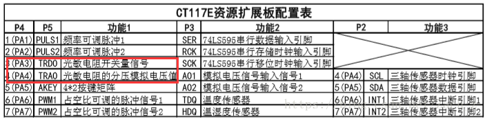
The direct initialization of PA3 is reading
void DO_Config(void)
{
	GPIO_InitTypeDef GPIO_InitStructure;

	RCC_APB2PeriphClockCmd(RCC_APB2Periph_GPIOA, ENABLE);

	GPIO_InitStructure.GPIO_Pin = GPIO_Pin_3;
	GPIO_InitStructure.GPIO_Speed = GPIO_Speed_2MHz;
	GPIO_InitStructure.GPIO_Mode = GPIO_Mode_IPU;
	GPIO_Init(GPIOA, &GPIO_InitStructure);
}
If the initialization of PA4 is ADC, I will not write it.
4. Objective questions
4.1 on chip resources
The on-chip resources can be found through the data book. For details, you can open the test room to provide the data book "stm32f103rbt6.pdf" to view: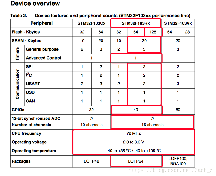
- 128K flash
- 20K SRAM
- 3 general timers (TIM2, TIM3, TIM4)
- An advanced timer (TIM1)
- 2 SPIs (SP1, SPI2)
- 2 I2C (I2C1, I2C2)
- 3 USARTs (usart1, USART2, USART3)
- 1 USB 2
- 1 CAN 2.0B
- 49 GPIO ports
- Two (12 bit ADC modules), all 16 channels
- The CPU frequency is 72MHz
- Working voltage: 2.0~3.6V
- Working temperature: - 40 ~ + 85 / - 40 ~ + 105
- Package form: LQFP64
4.2 possible stm32 knowledge
It is possible to find all the basic test results in the data manual. The English version of the manual should be provided during the competition. I suggest that you read all the manuals before the competition, at least to know where to find the corresponding knowledge points.
4.2.1 nested vector interrupt controller (NVIC)
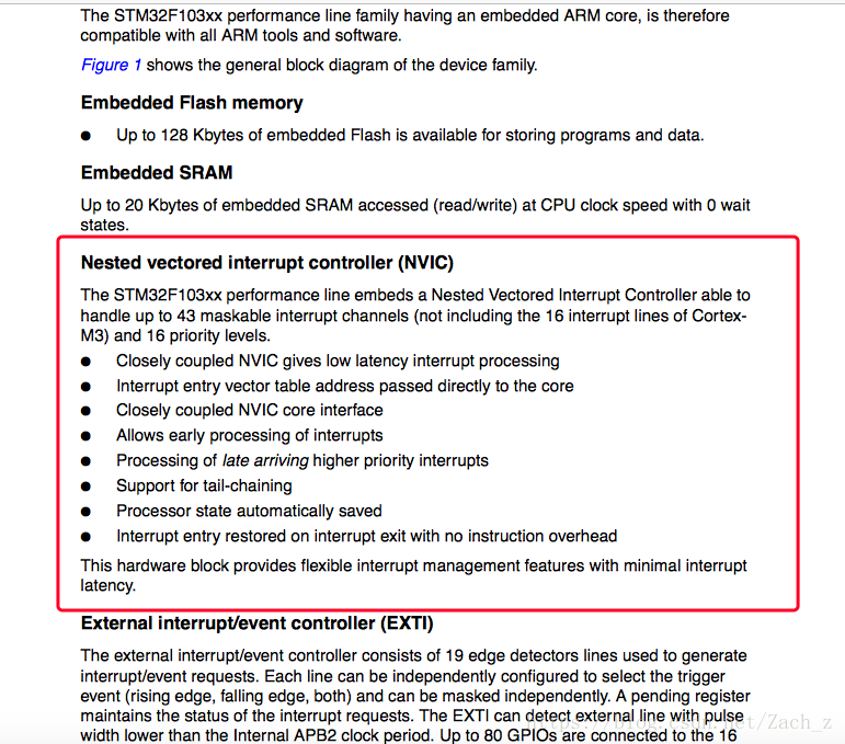
STM32F103xx enhanced product has built-in nested vector interrupt controller, which can handle up to 43 maskable interrupt channels (excluding 16 Cortex Gamma -M3) and 16 priorities.
- Tightly coupled NVIC enables low latency interrupt response processing
- Interrupt vector entry address directly into the kernel
- Tightly coupled NVIC interface
- Allow early processing of interrupts
- Handle late higher priority interrupts
- Support the function of breaking tail link
- Automatically save processor state
- Automatic recovery on interrupt return without additional instruction overhead
Remember 16 priorities, 5 priority groups
4.2.2 external interrupt / event controller (EXTI)
The external interrupt / event controller contains 19 edge detectors for generating interrupt / event requests. Each interrupt line can independently configure its triggering events (rising edge or falling edge or double edge), and can be individually shielded; there is a pending register to maintain the status of all interrupt requests. EXTI can detect that the pulse width is less than the clock period of internal APB2. Up to 80 universal I/O ports are connected to 16 external interrupt lines.
4.2.3 clock and start
The selection of the unified clock is carried out at startup. During reset, the internal 8MHz RC oscillator is selected as the default CPU clock, and then the external 4-16mhz clock with failure monitoring can be selected;
When the external clock fails, it will be isolated and the system will automatically switch to the internal RC oscillator. If the interrupt is enabled, the software can receive the corresponding interrupt.
Similarly, complete interrupt management of PLL clock can be adopted when necessary (such as when an indirectly used external oscillator fails).
Multiple prescalers are used to configure the frequency, high-speed APB(APB2) and low-speed APB(APB1) areas of the AHB.
The highest frequency of AHB and high-speed APB is 72mhz, and the highest frequency of low-speed APB is 36MHz. TIM up to 72mhz
Refer to the clock drive block diagram as shown in the figure:
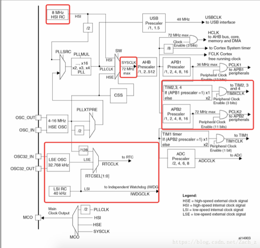
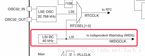
The most important thing is to find the relationship between the clock source and the corresponding equipment through the clock block diagram:
For example, the 40 kHz RC oscillator HSI serves as the clock source of the independent watchdog (IWDG):
4.2.4 DMA
DMA is basically a must in the objective questions, because DMA is an important means of transmission in embedded system, and the subjective questions are not easy to investigate, so we will certainly examine the corresponding knowledge points of DMA in the objective questions
Flexible 7-way universal DMA can manage the data transfer from memory to memory, device to memory and memory to device; DMA controller supports the management of ring buffer, avoiding the interrupt when the controller transfers to the end of buffer.
Each channel has a special hardware DMA request logic, and each channel can be triggered by software at the same time; the transmission length, transmission source address and destination address can be set separately by software.
DMA can be used in the main peripherals: SPI, I2C, USART, TIMx and ADC.
The DMA of STM32 has the following characteristics:
- Each channel is directly connected to a dedicated hardware DMA request, and each channel also supports software triggering. These functions are configured by software.
- The priority among the seven requests can be set by software programming (four levels in total: very high, high, medium and low), if it is determined by hardware when the priority is equal (request 0 is prior to request 1, and so on).
- The transmission width (byte, half word, full word) of independent source and target data area simulates the process of packaging and unpacking. The source and destination addresses must be aligned with the data transfer width.
- Buffer management supporting loop
- Each channel has three event flags (DMA half transfer, DMA transfer completion and DMA transfer error). These three event flags logic or become a separate interrupt request.
- Transfer between memory and memory
- Peripheral and memory, memory and peripheral transmission
- Flash memory, SRAM, SRAM of peripherals, APB1 APB2 and AHB peripherals can be used as the source and target of access.
- Number of programmable data transfers: 65536 maximum
4.2.5 watchdog
4.2.5.1 independent watchdog
The independent watchdog is based on a 12 bit decrement counter and an 8-bit prescaler. It is provided with a clock by an internal independent 40 kHz RC oscillator;
Since the RC oscillator is independent of the master clock, it can operate in shutdown and standby mode. It can be used as a watchdog to reset the entire system in the event of a problem, or as a free timer to provide timeout management for applications.
The option byte can be configured to be a software or hardware boot watchdog. In debug mode, counters can be frozen.
4.2.5.2 window watchdog
**There is a 7-bit decrement counter in the watchdog, which can be set to run freely. It can be used as a watchdog to reset the entire system in the event of a problem.
It is driven by the master clock and has the function of early warning interrupt; in the debugging mode, the counter can be frozen
4.3 other knowledge
Objective questions can't be completed quickly, or they are usually accumulated. We can only understand some aspects with pertinence
- The difference between synchronous communication and asynchronous communication
- Storage system of embedded system
- The difference between serial bus and parallel bus
- Knowledge of real time operating system
- Knowledge of array circuit
- Knowledge and calculation of analog circuits (mainly diodes, triodes, operators, amplifiers)
The more knowledge you have, the better
5. Competition experience
5.1 remember the function of each pin
There are only 8 pins (PA1-7) that can be connected externally, and the pins connected with the expansion board drive all peripheral devices of the expansion board
I believe that in the process of practicing the match simulation, the brain will gradually become more and more familiar with PA1-7.
Although we can find the corresponding functions of these pins and the corresponding clock channels in the corresponding manuals, we hope to have the following table in our mind:
| GPIO | function |
|---|---|
| PA1 | TIM2? CH2 / Ser (74ls595 serial data input pin) / frequency adjustable pulse |
| PA2 | TIM2? CH3 / usart2? TX / RCK (74ls595 serial storage clock input pin) / frequency adjustable pulse |
| PA3 | Usart2? Rx / sck (74ls595 serial shift clock input pin) / photoresistor read in pin |
| PA4 | ADC1? In4 / SCL (three axis sensor clock pin) |
| PA5 | ADC1 ﹣ in5 / SDA (three axis sensor data pin) / 4 * 2 key matrix |
| PA6 | Tim3 Chu ch1 / duty cycle adjustable pulse / temperature sensor |
| PA7 | Tim3 Chu CH2 / duty cycle adjustable pulse / temperature and humidity sensor |
5.2 how to prepare
Overall route:
- First of all, understand each independent driver, and be able to write and use it smoothly
- Next, I will do the simulation, provincial and national competitions of the previous years
- In the end, I gave myself a question, which I thought might be tested, but I didn't test in the previous years
5.2.1 fast write driver
If you look at the writing of each driver code above, you can know that we don't need to type most of the code ourselves.
In the Example of the library function provided by the game, there is the code that we need to drive basically. We just need to change it to what we need (clock, pin, etc.).
If you forget how to write some functions, you can also find the header file of the corresponding library function.
5.2.2 start again every time you do a new question
I hope that every time I do a subjective question again, I can write the code on the logic layer from the most basic LCD driver reference routine, and do not copy and paste it.
Because the game is different from the usual things, even if you think you understand the principle and drive, you know how to write. If you don't do it very skillfully, small mistakes will inevitably occur, and small mistakes may delay a lot of time, so you must be careful.
So now that we have chosen to participate in the competition, we hope that the better we are prepared, the faster we can write the basic driver, and the better we are familiar with each module
5.2.3 there should be a plan for the allocation of preparation time
If you are Xiaobai, I suggest you learn other stm32 tutorials first, because there are too few reference materials for this contest, but you need to know the principle a lot when writing 32, and then start to contact this contest.
If you have a certain development foundation of stm32 or other embedded devices, match preparation time will be allocated according to your learning ability
It took about two weeks before the competition in our province, which is roughly divided as follows:
- Prepare my widget in the first week (LED - > systick (delay ﹐ ms()) - > key - > LCD - > ADC - > RTC - > USART - > E2PROM (I2C))
- In the second week, I began to practice the previous questions, and did some simulation questions and provincial competition questions from the 5th to 9th sessions
- At the beginning of doing simulation questions, it will be very slow. It will take 7 or 8 hours to complete the task. After two or three sessions of training, I will be more and more comfortable. Later, I wrote a task every night
5.3 how to compete
5.3.1 do not leave in advance
There are always some students leaving the field ahead of time in the game. I don't know if they are confident or can't give up directly
I think since I have chosen to play and have done so much preparation before the match, I should try my best to finish the match
If you have done all the tasks of the program, feel that the game is stable:
- You can check your own objective questions again. After all, above the second level of our country are all on the objective questions
- You can also check your own programs and test several groups of data to see if there are any bug s
- You can also modify the code, simplify the algorithm, and add comments
In a word, it's only for these five hours to prepare for a few weeks. It's not worth it to leave ahead of time
5.3.2 plan the distribution of competition time
Every place of the Provincial Games is different, and may not allow early entry. I will assume 5 hours:
-
After getting the questions, first look at the subjective questions and leave an impression in my heart
-
When we start to do the objective questions, the objective questions usually don't take much time. It's 20 minutes. When we do the objective questions, our brain also thinks about the framework of the subjective questions
-
After finishing the objective questions, remember to submit them once and start the subjective question writing procedure
-
If it's done in advance, of course, it's good to check, optimize and check all possible bug s
-
If there is still half an hour to write before the end of the competition, first make the existing program into a program that can run smoothly without downtime, and submit it again
-
Make sure you submit the objective questions and procedures at the end of half an hour. First, make sure you have a score
In general, the National Games can be entered half an hour ahead of schedule, and those who are in line early can enter more than ten minutes earlier than the last, so try to win more than ten minutes as early as possible: -
After entering the site in advance, the board is usually delivered. When I went there, the board was next to me. So we can use these 20 minutes to test the burn-in screen routine to see if the board is normal, and then write a drive of LED, key and ADC (LED, key must be tested, 90% of ADC)
-
Make full use of the time to enter the site. If you do well, you should be able to complete the work of LED, button and ADC
-
After getting the contest questions, first look at the subjective questions, do the objective questions directly, and remember to submit them after finishing
-
Be sure to be optimistic about how to submit the program. Don't be wrong, or you will lose more than you gain
-
The second half hour of the National Games will be messy, and many people will leave early, so it's still half an hour from the end to adjust the procedures. We must submit all objective questions and procedures once
Again, explain the importance of half an hour from the end of the submission:
- The second half hour is the peak time of submission, and the match point server is congested. If you submit in the last few minutes, there may be unsuccessful submission, so we need to submit it again later to avoid accidents
- In the second half of an hour, many people hand in their papers and leave in advance. They come and go in and out. In case any Muggle touches your power cord, GG directly
- In theory, there won't be any big changes in the second half hour, but after you submit it once, at least you have a bottom in mind and won't be very flustered. Maybe there will be breakthroughs and unsolved problems will be solved
5.3.3 never give up in case of problems
All competitions will basically encounter problems: ACM, electric games, and the Blue Bridge Cup we participated in are all the same, with big or small problems
To be clear:
- If winning a prize without any difficulty proves that your level is higher than this competition, then you deserve to win the prize and are not happy
- When facing problems, difficulties and solutions, the happiest thing is to succeed in the end
When encountering problems, we must use our own knowledge and training experience to solve them step by step, calmly analyze them, and don't give up
6, gossip
Come on, the 10th National Championship national special prize is a Huawei laptop. It's not bad, especially the free 4-day tour in Beijing. It's exciting, but (the first prize is Sogou recorder,,,,, / / spitting blood).
Finally, some objective questions are attached
1. STM32F103RBT6 has (20) kByte RAM space, (128) Kbyte Flash space, (3) USART, (2) 12 bit ADC.
Analysis: read the first page of STM32? MD series data manual. You can't remember it or memorize it. Now you can use it for reference.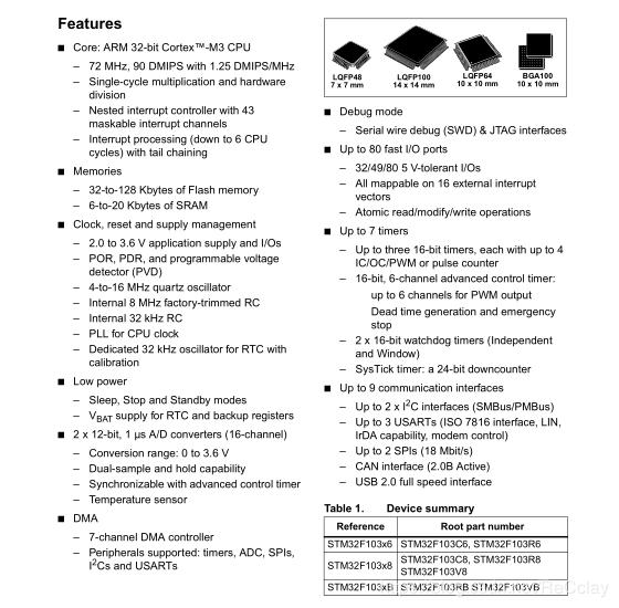
2. Meaning of each parameter in STM32 F 103 C 8 T 6 A
F = general type
103 = Enhanced
101 = Basic
102 = USB basic, USB 2.0 full speed device
105 or 107 = interconnected
T = 36 feet
C = 48 feet
R = 64 feet
V = 100 feet
Z = 144 feet
4 = 16K flash memory
6 = 32K
8 = 64K
B = 128K
C = 256K
D = 384K
E = 512K
H = BGA
T = LQFP
U = VFQFPN
Y = WLCSP64
6 = -40°C ~ 85°C
7 = -40°C ~ 105°C
A or blank (internal code, see product data manual for details)
3, Which of the following methods or tools can be used for program download (ABCD) of STM32
A. J-link
B. Co-Link
C.USART ISP
D.USART IAP
Resolution: J-link is the most commonly used one here. Even if co link didn't know it before, it should know that the embedded game with blue bridge is ready now. For USART-ISP, think about the fly MCU of punctual atom, which is probably that thing. Download the software of hex. USART-IAP is used to update the program. Please refer to here.
4. Which of the following descriptions are the features of STM32 GPIO (ABCD)
A. Separate bit setting, clearing
B. External break line / wake-up line
C. Reuse function and remapping
D. GPIO locking mechanism
Analysis:...
5. Analog signal acquisition equipment, ADC reference voltage is 5V, resolution is required to reach 5mV, ADC should select at least (B)
A. 8 bits
B. 10 bits
C. 12 bits
D. 16 bits
Resolution: how do I remember when the Blue Bridge Cup single chip microcomputer competition also has this question?
5V / 5mV = 1000, roughly divided into 1000 parts. And 2 ^ 10 = 1024, is also more than 1000 copies
6. The maximum number of data transfers programmable by STM32 DMA controller is (D)
A. 65536
B. 4096
C. 1024
D. 65535
Analysis: the series of single-chip 1 DMA, including 7 channels. Each channel is directly connected to a dedicated hardware DMA request, and each channel also supports software triggering, and priority can also be set. Each channel has three event flags (DMA half transfer, DAM transfer complete, DMA transfer error) to request an interrupt. The amount of data transmitted by the channel is programmable, with a maximum of 65535 bytes.
7. A system needs to store a small number of (less than 1K byte) parameters permanently and access them frequently. The most suitable memory is (B)
A. SRAM
B. E2PROM
C. Nor Flash
D. Nand Flash
Analysis: a small amount of data, of course, put EEPROM access is better.
8. The power supply of the operational amplifier is connected to ± 12V, the stable voltage of the regulator is 6V, and the forward conduction voltage is 0.6V. When the input voltage Ui = -2V, the output voltage UO should be (C)
A. -6V B. -2V
C. +6V D. 0.6V
Analysis: negative phase terminal - 2V, positive phase terminal 0V, so the output is + 12V, and because the regulator acts on the output, so the output is + 6V
9. Which of the following operating systems is suitable for STM32 series microcontroller (AB)
A. μCos-II
B. Free RTOS
C. Windows CE
D. Linux
Analysis:...
10. A voltage regulator is provided in STM32, which is always enabled after reset. It works in three different modes (ABC) according to the application mode. (multiple selection)
A. Operation mode
B. Stop mode
C. Standby mode
D. Low power mode
Analysis:
Operation mode: the regulator provides 1.8V power supply (core, memory and peripheral) in normal power consumption mode;
Stop mode: the regulator provides 1.8V power supply in low power consumption mode to save the contents of registers and SRAM;
Standby mode: the regulator stops power supply. Except for the spare circuit and backup domain, the contents of register and SRAM are all lost. < reference >
11. Low power consumption mode other than STM32 is (D).
A. Sleep mode
B. Stop mode
C. Standby mode
D. Operation mode
Analysis: three kinds of low power consumption: sleep, stop and standby
Sleep mode: Cortex-M3 core stops, and all peripherals including Cortex-M3 core peripherals, such as NVIC and SysTick, are still running;
Stop mode: all clocks are stopped.
Standby mode: 1.8V core power off. < Reference resources>
12. In stop mode, which of the following is correct (ABC). (multiple selection)
A. All clocks in the 1.8V supply area are stopped
B. PLL, HIS and HSE RC oscillator functions will be disabled
C. SRAM and register contents will be preserved
D. SRAM and register contents will be lost
Resolve: stop will still save the contents of SRM.
13. Each DMA channel has (A) event flags.
A.3
B.4
C.5
D.6
Resolution: each channel has three event flags: DMA half transfer, DAM transfer complete, DMA transfer error.
14. In DMA controller, the transmission width of independent source and target data area is (ABC) (multiple choice).
A. byte
B. half word
C. full word
D. None of the above
Analysis: look at the data to verify that it is true that byte, half word and whole word are OK.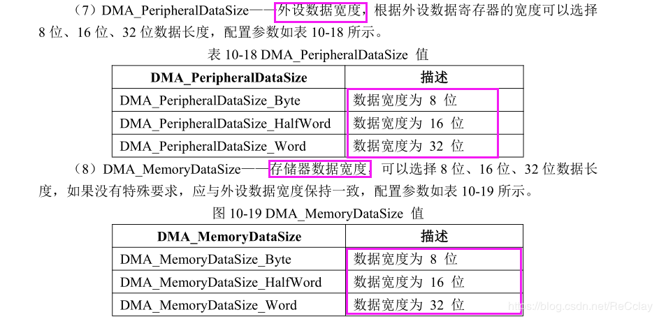
15. In STM32, one DMA request occupies at least (B) cycles of CPU access system bus time.
A.1
B.2
C.3
D.4
Analysis: remember
16. In STM32, the backup register is the register of (A).
A.16 bit
B.32 bit
C.8 bit
D.4 bit
Analysis: STM32 has backup registers, but the number of backup registers is not necessarily the same! For large capacity (HD) microprocessor series, it has 42 16 bit backup registers, while small and medium capacity microprocessors have only 10 16 bit backup registers. Generally speaking, the backup registers are all 16 bits.
17. In order to allow access to the backup register and RTC, the DBP bit of the power control register (PWR? CR) must be set to (A).
A.1
B.2
C.0
D.3
Resolution: enable (Set 1) after the backup area clock, enable the DBP bit of the PWR ﹣ CR register of the power supply to cancel the write protection of the backup area.
18. Which of the following is not a backup register.
A.BKP_DR1
B.BKP_DR3
C.BKP_RTCCR
D.BKP_DR5
Analysis: remember
19. If the watchdog WWDG is activated, A reset occurs when the value of the decrement counter is less than (A).
A.0x40
B.0x70
C.0x4F
D.0x7F
Analysis: the data can be verified
20. Write (A) in register IWDG_KR to start enabling the independent watchdog.
A.0xCCCC
B.0xBBBB
C.0xAAAA
D.0xDDDD
Analysis: refer to relevant materials
21. If the window watchdog starts and the counter (A) is decremented by 7 bits (T[6:0]), A reset action is generated.
A. Flip from 0x40 to 0x3F
B. Flip from 0x50 to 0x4F
C. Flip from 0x60 to 0x5F
D. Flip from 0x70 to 0x6F
Analysis: look at the figure of question 19
22. Time base unit of STM32 programmable TIM1 timer includes (ABCD). (multiple selection)
A. Counter register (TIM1? CNT)
B. Prescaler register (TIM1? PSC)
C. Autoload register (TIM1? ARR)
D. Cycle count register (TIM1? RCR)
Analysis: the basis of TIM
23. Features of advanced timer TIM1 (ABCD). (multiple selection)
A. With 16 bit up, down, up / down automatic loading counter
B. With 16 bit programmable prescaler.
C. The timer register can be updated after a specified number of counter cycles.
D. Interrupt can be generated by event, with rich interrupt types and DMA function
Analysis: characteristics of advanced timers
24. The special working mode of timer TIM1 includes (ABCD). (multiple selection)
A. Input capture mode
B. PWM input mode
C. Encoder interface mode
D. Single pulse mode (OPM)
Analysis: four working modes of timer
25. The time base unit of the programmable universal timer of STM32 includes (ABC). (multiple selection)
A. Counter register (timx? CNT)
B. Prescaler register (timx? PSC)
C. Autoload register (timx? ARR)
D. None of the above
Analysis: the same as 22 questions
26. ARM Cortex-M3 cannot wake up CPU through (D).
A. I/O port
B. RTC alarm clock
C. USB wake up event
D.PLL
Resolution: remember
27. STM32 nested vector interrupt controller (NVIC) has (A) programmable priority levels.
A.16
B.43
C.72
D.36
Analysis: previous records< link>
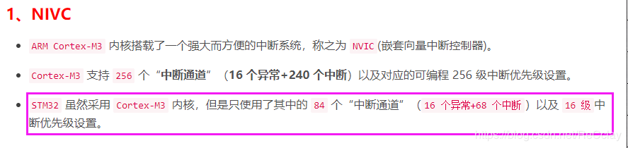
28. The external interrupt / event controller (EXTI) of STM32 supports (C) interrupt / event requests.
A.16
B.43
C.19
D.36
Resolution: refer to positive point atom STM32F1 Development Guide - library function version ﹣ V3.1
The interrupt controller of STM32F103 supports 19 external interrupts/
Event request. Each interrupt has a status bit, and each interrupt / event has its own trigger and mask settings. STM32F103
19 external interrupts are:
Line 0-15: input interruption corresponding to external IO port.
Line 16: connected to PVD output.
Line 17: connect to RTC alarm events.
Line 18: connect to USB wake up event.
Note that there are 16 interrupt lines for IO port.
29. Which are the characteristics of STM32 ADC system (ABCD). (multiple selection)
A. 12 bit resolution
B. Self calibration
C. Programmable data alignment
D. Single and continuous conversion mode
Analysis: basic knowledge of ADC
30. In the scan mode of ADC, if DMA bit is set, DMA controller will transfer the conversion data of regular group channel to (A) after each EOC.
A.SRAM
B.Flash
C. ADC? Jdrx register
D.ADC_CR1
Resolution: remember
31. STM32 rule group consists of up to (A) transformations.
A.16
B.18
C.4
D.20
Resolution: the rule group can use up to 16 channels, and the injection group can use up to 4 channels.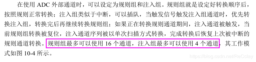
32. In STM32, the ALIGN bit of (A) register selects the alignment method of data storage after conversion.
A.ADC_CR2
B.ADC_JDRx
C.ADC_CR1
D.ADC_JSQR
Resolution: ALIGN bit in register ADC ﹣ CR2
33. Flash flash programming of STM32 can write (A) bit at A time.
A.16
B.8
C.32
D.4
Resolution: STM32 internal FLASH operation fixed 16 bits at a time, remember. < link>
34. The page size of STM32 main memory block is (A) bytes.
A.1K
B.3K
C.2K
D.4K
Analysis: STM32 is divided into four types of products: small capacity, medium capacity, large capacity and interconnection type according to the different capacity of FLASH main memory block, pages and system memory.
The main storage block of small capacity product is 1-32KB, 1KB per page. System storage 2KB.
The main memory block of medium capacity product is 64-128KB, 1KB per page. System storage 2KB.
The main storage block of large capacity product is more than 256KB, 2KB per page. System storage 2KB.
The main storage block of interconnected products is more than 256KB, 2KB per page. The system memory is 18KB.
35. The size of bytes selected by the user is (A).
A. 512 bytes
B.2K
C.1K
D.128K
Analysis: remember
36. Which of the following are not features of STM32 flash memory (C).
A. Large capacity
B. high speed
C. Power down without saving
D. With selection byte loader
Analysis: contents of FLSH
37. The turning speed of I/O pin on APB2 is (A).
A.18MHz
B.50MHz
C.36MHz
D.72MHz
Analysis: remember< link>
38. Timer 2's TIM2 "remap [1:0] is a remapping of" 10 "and" 11 ", which is suitable for (ABD) packaged chips.
A.64 pin
B. 100 pin
C.36 pin
D. 144 pin
Resolution: it is clearly stated in the manual that the re image is not applicable to the encapsulation of 36 pin. Refer to P119 of STM32 Chinese reference manual ﹖ V10
39. Remapping of USART2 ﹣ remap = 1 of USART2 is only applicable to the packaging of (BD) pin.
A.64 pin
B. 100 pin
C.36 pin
D. 144 pin
Analysis: according to the reference manual
40. When the output mode bit MODE[1:0] = "10", the maximum output speed is (B).
A.10MHz
B.2MHz
C.50MHz
D.72MHz
Resolution: the output rate of two bits corresponding to MODE can be found in the data, which is 2M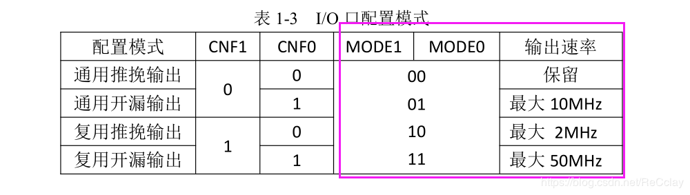
41. Which of the following is not a feature of RealView M D K development environment.
A. Windows style
B. Compatible Keil μ Vision interface
C. Comprehensive ARM processor support
D. Bulky
Analysis:...
42. Which of the following methods can be used for program download (ABC) of STM32. (multiple selection)
A.Keil ULink
B.J-Link
C. In application programming
D. None of the above
Analysis:...
43. The USART of STM32 selects to send 8-bit or 9-bit data words according to the status of M-bit in (A) register.
A.USART_CR1
B.USART_CR2
C.USART_BRR
D.USART_CR3
Resolution: remember to set the number of data bytes: CR1 register, set the number of stop bits determined by CR2
44. The main working mode of bxCAN of STM32 is (ABCD).
A. Initialization mode
B. Normal mode
C. Loopback mode
D. Sleep mode
Resolution: remember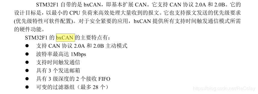
45. In the program, you can set the (AB) bit of the can? BTR register to 1 at the same time to enter the loopback silent mode. (multiple selection)
A.LBKM
B.SILM
C.BTR
D. None of the above
Analysis: remember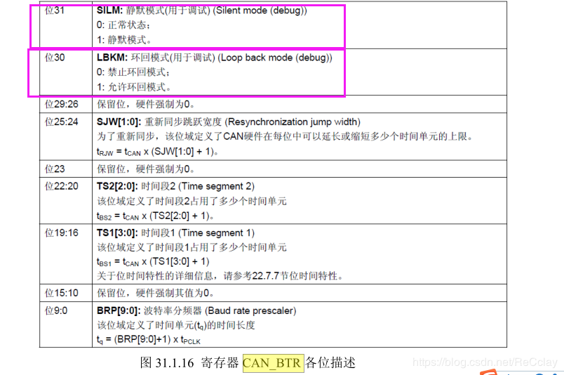
46. STM32 provides three different clock sources, all of which can be used to drive SYSCLK. The three clock sources are (ABC).
A. HSI oscillator clock
B. HSE oscillator clock
C. PLL clock
D. HLI oscillation clock
Analysis:...
47. In STM32, when (AB) occurs, a power reset will be generated. (multiple selection)
A. Return from standby mode
B. Power on / power off reset (POR/PDR reset)
C. Low level on NRST pin
D.PLL
Analysis: attention is power reset, new knowledge
48. Which of the following clock signals can be selected as the MCO clock (ABCD). (multiple selection)
A.SYSCLK
B.HSI
C.HSE
D. PLL clock with 2 division frequency
Analysis: MCO clock, emmm, another new knowledge point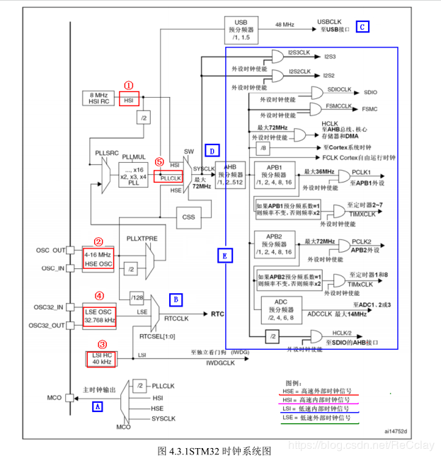
Corresponding to the above figure, A is the MCO clock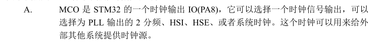
reference:
https://blog.csdn.net/Zach_z/article/details/80548423
https://blog.csdn.net/ReCclay/article/details/86699835

