When it comes to FPGA serial port code, it's very different from SCM. SCM's serial port is relatively simple. It only needs register configuration of existing serial port module, but for FPGA, it's much more complex. It's similar to building a serial port receiving module from scratch. Now we'll take an example to illustrate
We need to understand what we need to do from the serial port protocol. In short, we need to construct the following waveform detection. In my eyes, this is very similar to the serial port implementation of MCU io simulation with timer, so it is also very complex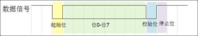
First of all, in daily life, the data signal is 1, so there is no need to operate at this time. However, after the falling edge is detected, the detection will start. Because of the asynchronous characteristics of the serial port, it completely depends on the time of high and low level to judge, such as the baud rate 115200, which corresponds to 8.68us. In the case of my FPGA 50Mhz (T=0.02us), when the counter is 434, the end of a signal can be determined, For the sake of safety, the sampling level is the most stable in the middle of the signal
If we understand the principle, we need to design according to the function
1. First, we need a timer module of serial port. Once the falling edge signal is received, it starts to work. Then, we give two FLAG bits to end at the sampling point (middle point) and a bit
2. Secondly, we need a serial processing module, which has to complete the following functions
(1) Detect the falling edge signal and inform the serial port to turn on the timer
(2) Sampling data: an 8-bit register used to store data, which samples when the FLAG at the midpoint arrives, and moves left
(3) A counter is needed to count the number of bits and stop receiving when the count is complete
3. Map the acquired 1234567890 data to the frequency of the buzzer (do not expand)
Note: the design process should first design from the top level to get the top level input and output, then divide them into blocks according to the function, then describe the input and output of each module, after dividing the blocks, find out the output and input of each block, then put them on the top level design for example, and finally fill in the content of each block
The top level code is as follows:
module uart(
CLK_50M,RST_N,UART_RX,
UART_TX,BEEP
);
//External port definition
input CLK_50M,RST_N,UART_RX;
output BEEP,UART_TX;

//Definition of internal wiring
wire              rx_bps_start;//RX module controls the enabling of bps
wire              rx_bps_flag;//RX module receives the sample point flag. Although it is defined differently in bps and Rx files, it is essentially a line that only needs to be defined once in the main file
wire              BEEP;
wire 					tx_bps_start;			//Baud rate clock start signal of send port (not used by this routine)
wire     [7:0 ]   out_rx_data;

bps_module		Uart_Rx_Bps_Init
(
	.CLK_50M				(CLK_50M			),	//Clock port
	.RST_N				(RST_N			),	//Reset port
	.bps_start			(rx_bps_start	),	//Baud rate clock start signal of receiving port
	.bps_flag			(rx_bps_flag	)	//Intermediate sampling point for receiving data bits
);

//Example receiving module
rx_module			Uart_Rx_Init
(
	.CLK_50M				(CLK_50M			),	//Clock port
	.RST_N				(RST_N			),	//Reset port
	.UART_RX				(UART_RX			),	//Receive port of FPGA, send port of serial port CP2102
	.rx_bps_start		(rx_bps_start	),	//Baud rate clock start signal of receiving port
	.rx_bps_flag		(rx_bps_flag	),	//Intermediate sampling point for receiving data bits
	.out_rx_data		(out_rx_data	)	//Output received data
);
beep_module				Beep_Init
(
	.CLK_50M				(CLK_50M			),	//Clock port
	.RST_N				(RST_N			),	//Reset port
	.BEEP					(BEEP				),	//Buzzer port
	.KEY					(out_rx_data	)	//Output the received data to the buzzer module
);
endmodule
Timer module
module bps_module(
CLK_50M,bps_start,RST_N,
bps_flag
);
//I / O port definition
input CLK_50M;
input bps_start;
input RST_N;//Start? Flag, RX module control timer enabled
output bps_flag;//Sampling midpoint, output to RX module
endmodule
RX module
module rx_module(
CLK_50M,RST_N,rx_bps_flag,UART_RX,
rx_bps_start,out_rx_data
);
input CLK_50M;
input RST_N;
input rx_bps_flag;//RX ﹣ BPS ﹣ flag is the sampling flag bit, UART ﹣ Rx is the serial port receiving line
input UART_RX;
output rx_bps_start;//RX start flag is used to enable the timer bps module, and out RX data is used to enable the external module
output [7:0 ]out_rx_data;


endmodule
Buzzer module
module beep_module(
CLK_50M,RST_N,KEY,
BEEP
);
input CLK_50M,RST_N;
input [7:0] KEY;//key corresponds to the data obtained by serial port
output BEEP;//Buzzer control pin
endmodule
The advantage of this method is that it can compile directly and then generate RTL. You can see the wiring clearly. In this part, we complete the design of the top module and the signal wiring between the modules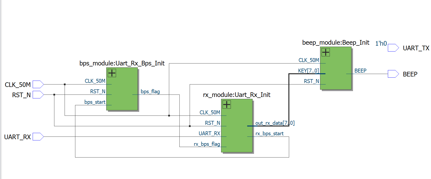
tips: it's better to write one line for input and output, otherwise it's not clear enough
The module itself is filled in as follows
First, the timer part of the serial port
module bps_module(
CLK_50M,bps_start,RST_N,
bps_flag
);
//Definition of external I / O port
input CLK_50M;
input bps_start;
input RST_N;//bps_start, RX module control timer enable
output bps_flag;//Sampling midpoint, output to RX module

//Internal port definition
reg [12:0] time_cnt;//Counter
reg [12:0] time_cnt_n;//Counter next status
reg bps_flag;
reg bps_flag_n;

//Parameter setting
parameter BPS_PARA=4'd434;
parameter BPS_PARA_HALF=4'd217;


//Timer Description: the value of the register needs to be increased by adding one at a time through the adder, and the current value will be updated whenever a rising edge pulse arrives, so
//This register is composed of a 13 bit D flip-flop. The sequential logic circuit is only used to update the value of the D flip-flop. The combined logic circuit between the output and the input is used to add one. This part is written separately
//The advantage is that the code on the timing side will be extremely simple, only the value after the change of the combinational logic circuit needs to be updated
//Sequential logic circuit
always @(posedge CLK_50M or negedge RST_N)
begin
if(!RST_N)
    time_cnt=13'b0;
else
    time_cnt<=time_cnt_n;
end
//Combinational logic circuit
always @(*)
begin
if((!bps_start)&&(time_cnt==BPS_PARA))
   time_cnt_n=13'b0;
else
   time_cnt_n=time_cnt_n+1'b1;
end
//Sequential logic circuit
always @(posedge CLK_50M or negedge RST_N)
begin
if(!RST_N)
    bps_flag=1'b0;
else
    bps_flag<=bps_flag_n;
end
//Combinational logic circuit: if the count reaches BPS ﹣ para ﹣ half, it indicates that the sampling point is reached, and the sampling can be performed
always @(*)
begin
if(time_cnt==BPS_PARA_HALF)
   bps_flag = 1'b1;
else
   bps_flag = 1'b0
end
endmodule
And then there's the RX module
module rx_module(
CLK_50M,RST_N,rx_bps_flag,UART_RX,
rx_bps_start,out_rx_data
);
//Definition of external I / O port
input CLK_50M;
input RST_N;
input rx_bps_flag;//RX ﹣ BPS ﹣ flag is the sampling flag bit, UART ﹣ Rx is the serial port receiving line
input UART_RX;
output rx_bps_start;//RX start flag is used to enable the timer bps module, and out RX data is used to enable the external module
output [7:0 ]out_rx_data;

//First of all, it is necessary to reserve the front and back level states of the falling edge for judgment. Therefore, the function of the two bit register is to keep the previous and current level states
reg		[ 1:0]	detect_edge;			//Record the start pulse of UART, i.e. the first falling edge
wire		[ 1:0]	detect_edge_n;			//Next state of detect edge
//Then when 10 is detected, a falling edge flag is needed to tell bps that the timer can be executed
reg					negedge_reg;			//Falling edge sign
wire					negedge_reg_n;			//Next state of nagedge? Reg
reg					rx_bps_start;			//Baud rate clock start signal of receiving port
reg					rx_bps_start_n;		//Next state of Rx? BPS? Start
//Number of accepted digits to be recorded
reg     [3:0]       bit_cnt;
reg     [3:0]       bit_cnt_n;
//Serial data buf
reg      [7:0]      shift_data;
reg      [7:0]      shift_data_n;
//Accept complete to save this data for use
reg		[ 7:0] 	  out_rx_data;			//Data after parsing from UART? RX data line
reg		[ 7:0] 	  out_rx_data_n;			//Next state of out? RX? Data

//The first step is to detect the falling edge
always @(posedge CLK_50M or negedge RST_N)
begin
if(!RST_N)
    detect_edge<=2'b11;
else
    detect_edge<=detect_edge_n;
end
//No data is always 11. Once the RX data is 0, the data will be 10
//Combined circuit for receiving UART? RX signal
assign detect_edge_n = {detect_edge[0], UART_RX};
//Check whether the data is 10 and turn on the falling edge flag bit
always @(posedge CLK_50M or negedge RST_N)
begin
if(!RST_N)
    negedge_reg<=1'b0;
else
    negedge_reg<=negedge_reg_n;
end

//Combined circuit, judge the falling edge. If the falling edge comes, the next edge is 1
assign negedge_reg_n = (detect_edge == 2'b10) ? 1'b1 : 1'b0;
//When the falling edge flag bit is 1, turn on the timer enable line
always @(posedge CLK_50M or negedge RST_N)
begin
if(!RST_N)
    rx_bps_start<=1'b0;
else
    rx_bps_start<=rx_bps_start_n;
end

always @(*)
begin
if(negedge_reg==1'b1)
	 rx_bps_start_n=1'b1;
else if(bit_cnt==4'd9)
    rx_bps_start_n=1'b0;
else
	 rx_bps_start_n=rx_bps_start;//If the number accepted is within 9, the data is not received completely, so keep 1
end

//Receive count enable, count once if the sample point is reached
always @(posedge CLK_50M or negedge RST_N)
begin
if((!RST_N))
    bit_cnt<=4'd0;
else
    bit_cnt<=bit_cnt_n;
end

always @(*)
begin
if(rx_bps_flag==1'b1)
   bit_cnt_n=bit_cnt+4'd1;
else if(bit_cnt==4'd9)
   bit_cnt_n=4'd0;
else
   bit_cnt_n=bit_cnt;
end

//Here is the data received by the store
always @(posedge CLK_50M or negedge RST_N)
begin
if((!RST_N))
    shift_data<=4'd0;
else
    shift_data<=shift_data_n;
end
//The method used is to move right. There are 9 times of right shift in total. Since the starting bit is only 0, the first right shift has no effect, and the reserved data is still 8 bits
always @(*)
begin
if(rx_bps_flag==1)
   shift_data_n[7:0]={UART_RX,shift_data[7:1]};
else
   shift_data_n=shift_data;
end

//Sequential circuit, used to assign value to out ﹣ Rx ﹣ data register
//I think it's necessary to add a register assignment. If you send shift all the time, it's similar to 9 times as a group to keep updating. If you use it directly, it may appear
//The register changes when it is used, so we need to make sure that the value after transmission is used
always @ (posedge CLK_50M or negedge RST_N)
begin
	if(!RST_N)									//Judgement reset
		out_rx_data <= 8'b0;					//Initialize the out? RX? Data value
	else
		out_rx_data <= out_rx_data_n;		//Used to assign values to out? RX? Data
end

//Combined circuit, if the data receiving is completed, the data in the shift register will be output
always @ (*)
begin
	if(bit_cnt == 4'd9)						//Judge whether the data has been received
		out_rx_data_n = shift_data;		//If the reception is complete, the data in the shift register is output
	else
		out_rx_data_n = out_rx_data;		//Otherwise, it will remain unchanged
end

endmodule
The Last Timer
//--------------------------------------------------------------------------- //--Filename: beep? Module. V //--Author: ZIRCON //--Description: buzzer sound module //--Revision history: January 1, 2014 //--------------------------------------------------------------------------- module Beep_Module ( //Input port CLK_50M,RST_N,KEY, //Output port BEEP ); //--------------------------------------------------------------------------- //--External port declaration //--------------------------------------------------------------------------- input CLK_50M; //Clock port, 50MHz crystal oscillator for development board input RST_N; //Reset port, low level reset input [ 7:0] KEY; //Keypad port output BEEP; //Buzzer port //--------------------------------------------------------------------------- //--Internal port declaration //--------------------------------------------------------------------------- reg [15:0] time_cnt; //Timing counter used to control the sound frequency of buzzer reg [15:0] time_cnt_n; //Next state of 44 time CNT reg [15:0] freq; //Frequency division value of various tones reg [15:0] freq_n; //Frequency division value of various tones reg beep_reg; //Register used to control the sound of buzzer reg beep_reg_n; //Next status of beep reg /* reg [13:0] time_on_cnt; reg [13:0] time_on_cnt_n; parameter beep_0 = 0; parameter cnt_on = 14'd10000; */ //--------------------------------------------------------------------------- //--Logic function realization //--------------------------------------------------------------------------- //Sequential circuit, used to assign value to time CNT register always @ (posedge CLK_50M or negedge RST_N) begin if(!RST_N) //Judgement reset time_cnt <= 16'b0; //Initialize time CNT value else time_cnt <= time_cnt_n; //Used to assign a value to time CNT end //Combined circuit, judge frequency, let timer accumulate always @ (*) begin if(time_cnt == freq) //Judge frequency division value time_cnt_n = 16'b0; //Timer reset operation else time_cnt_n = time_cnt + 1'b1; //Timer accumulation operation end //Sequential circuit to assign a value to the beep? Reg register always @ (posedge CLK_50M or negedge RST_N) begin if(!RST_N) //Judgement reset beep_reg <= 1'b0; //Initialize beep? Reg value else beep_reg <= beep_reg_n; //Used to assign a value to beep? Reg end //Combined circuit, judge frequency, make buzzer sound /* always @ (*) begin if(time_cnt == freq) //Judge frequency division value begin if(time_on_cnt == cnt_on) time_on_cnt_n = 14'd0; else beep_reg_n = ~beep_reg; //Change the status of the buzzer time_on_cnt_n = time_on_cnt + 14'd1; end else beep_reg_n = beep_0; //The status of the buzzer remains unchanged end */ always @ (*) begin if(time_cnt == freq) beep_reg_n = ~beep_reg; else beep_reg_n = beep_reg; end //Sequential circuit to assign a value to the beep? Reg register always @ (posedge CLK_50M or negedge RST_N) begin if(!RST_N) //Judgement reset freq <= 16'b0; //Initialize beep? Reg value else freq <= freq_n; //Used to assign a value to beep? Reg end //Combined circuit, press the key to select the frequency division value to realize the different sounds of the buzzer //The frequency of midrange do is 523.3hz, freq = 50 * 10^6 / (523 * 2) = 47774 always @ (*) begin case(KEY) 8'h30: freq_n = 16'd0; //No sound 8'h31: freq_n = 16'd47774; //Median 1 frequency value 262Hz 8'h32: freq_n = 16'd42568; //Midrange 2 frequency 587.3Hz 8'h33: freq_n = 16'd37919; //Median 3 frequency 659.3Hz 8'h34: freq_n = 16'd35791; //Midrange 4 frequency 698.5Hz 8'h35: freq_n = 16'd31888; //Midrange 5 frequency value 784Hz 8'h36: freq_n = 16'd28409; //Midrange 6 frequency value 880Hz 8'h37: freq_n = 16'd25309; //Midrange 7 frequency value 987.8Hz 8'h38: freq_n = 16'd23889; //Frequency value of treble 1 1046.5Hz 8'h39: freq_n = 16'd21276; //Frequency value of treble 2 1175Hz default : freq_n = freq; endcase end assign BEEP = beep_reg; //Finally, assign the value of the register to port BEEP endmodule

