Experimental objectives:
• master the interface timing of parallel DAC and ADC
• DDS is used to synthesize signals, which are output through DAC
• signal acquisition with ADC
• use SignalTAP to observe the signal in time domain
• observe the signal in the frequency domain using Matlab
Original experiment
50M crystal oscillator - through the phase-locked loop in FPGA chip - frequency doubling to obtain 80MHz DAC clock and frequency division to obtain 20MHz ADC clock
DAC clock: use the logic of FPGA to invert the internal 80MHz clock as the DAC chip clock to meet the establishment hold timing of DAC data
ADC clock: the ADC clock is also inverted as the driving clock of ADC interface logic

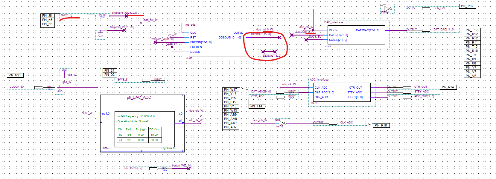
Write clock management module, DDS module, DAC module and ADC module respectively, and generate corresponding components
Connect the circuit and assign pins
- In this design, a PLL generates 80MHz DAC clock and 20MHz ADC clock from 50MHz crystal oscillator
- A single period DDS generates a complementary sine wave, which is converted into an unsigned sine wave and sent to the DAC
- The dial switch SW9 and SW8 are used to control the output amplitude of the DAC
- The remaining SW switches are used to control the DDS frequency word
Connect ADC and DAC with SMA coaxial cable
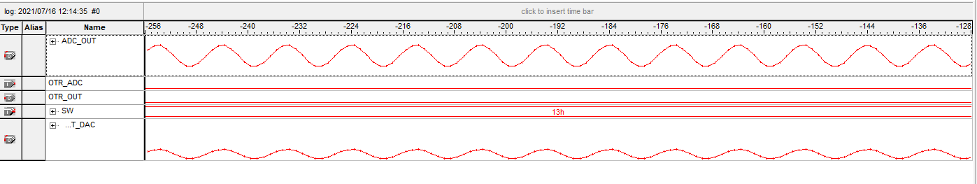
Grab ADC

ADC
dac
Answer to thinking questions

- It conforms to Nyquist theory. According to the spectrum diagram analyzed by matlab, the maximum frequency of analog signal is 0.5MHz, while the clock of ADC is 20MHz, which conforms to Nyquist theory
- It can be seen that the lowest noise of ADC is greater than the output of DAC.
- ADC is a process of sampling, holding, quantization and coding of analog signals, which makes them easier to store and process.
Supplementary knowledge
Student experiment
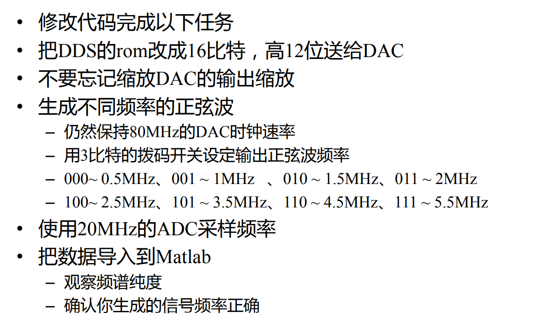
1. rom is changed to 16 bits, and the wave table file is automatically generated by matlab
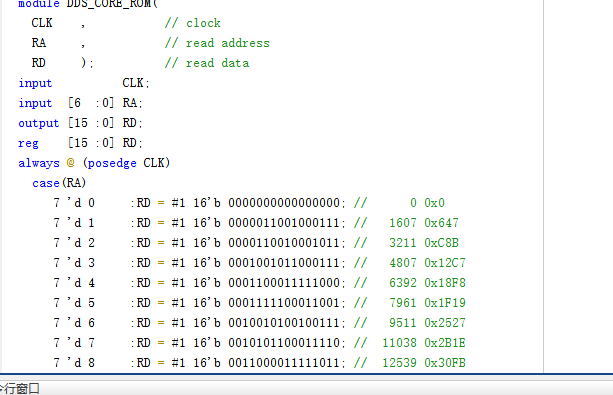
DDS code
The data and output are changed to 16 bits, and then different frequency words are assigned to different key inputs. The frequency word calculation method is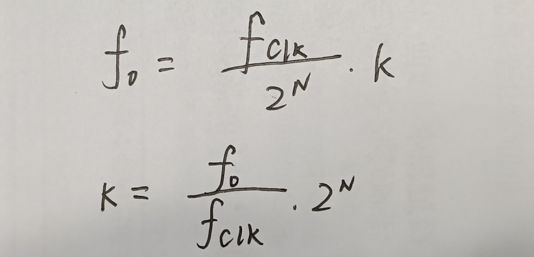
Then convert it to binary and assign it to freqin_R
module mc_dds(
  CLK   ,   // clock posedge
  RST   ,   // reset posedge
  FREQIN,   // input frequency word
  FREQEN,   // frequency word input enable
  DDSEN ,   // multi-cycle dds work enable
  OUTVD ,   // dds output valid
  DDSOUT);  // dds  output wave

input           CLK   ;
input           RST   ;
input  [32-1:0] FREQIN;
input           FREQEN;
input           DDSEN ;
output          OUTVD ;
output [11  :0]  DDSOUT;

// work enable delay line
reg ddsen_R1, ddsen_R2, ddsen_R3;

reg  [32-1:0]  freqin_R     ;
reg  [32-1:0]  phase_acc_R  ;
reg   [16-1:0]  DDSOUT       ;
wire  [16-1:0]  rom_rdW      ;   // rom read data
wire  [7-1:0]  rom_raW      ;   // rom read address
// code template
// always @ (posedge CLK or posedge RST) begin
//   if(RST) begin
//   end
//   else begin
//   end
// end

always @ (posedge CLK or posedge RST) begin
  if(RST) begin
    ddsen_R1 <= 1'b0;
    ddsen_R2 <= 1'b0;
    ddsen_R3 <= 1'b0;
  end
  else begin
    ddsen_R1 <= DDSEN   ;
    ddsen_R2 <= ddsen_R1;
    ddsen_R3 <= ddsen_R2;
  end
end
assign OUTVD = ddsen_R3;


// dds working pipeline
//                                       OUTVD
// DDSEN    | ddsen_R1     |ddsen_R2    |ddsen_R3
//          | phase_acc_R  |
//          | rom_raW      | rom_rdW    | DDSOUT
always @ (posedge CLK or posedge RST) begin
  if(RST) begin
    phase_acc_R <= 0;
    freqin_R    <= 0;
  end
  else begin
    if(FREQEN) begin
     case(FREQIN[24:22])
          3'b000:freqin_R <=32'b00000001100110011001100110011010;
          3'b001:freqin_R <=32'b00000011001100110011001100110011;
          3'b010:freqin_R <=32'b00000100110011001100110011001101;
          3'b011:freqin_R <=32'b00000110011001100110011001100110;
          3'b100:freqin_R <=32'b00001000000000000000000000000000;
          3'b101:freqin_R <=32'b00001011001100110011001100110011;
          3'b110:freqin_R <=32'b00001110011001100110011001100110;
          3'b111:freqin_R <=32'b00010001100110011001100110011010;

    endcase // if(FREQEN)
    end // if(FREQEN)
    if(DDSEN) begin
      phase_acc_R <= phase_acc_R + freqin_R;
    end // if(DDSEN)
    if(ddsen_R2) begin
      DDSOUT <= rom_rdW;
    end
  end
end
assign rom_raW = phase_acc_R[32-1: 32-1-7+1];

sine_rom U_sine_rom(
  .CLK    (CLK        ),  // clock
  .RA     (rom_raW    ),  // read address
  .RD     (rom_rdW    )); // read data

endmodule //  mc_dds();
DAC code
Note that the input becomes 12 bits and the 2 Complement becomes an unsigned number
module DAC_interface(
  CLKIN   ,   //  input clk
  DATIN   ,   //  input data
  SCALE   ,   //  scale factor, right shift the data
  DAT2DAC );   //  data to dac


input           CLKIN;
input  [12-1:0]  DATIN   ;
input  [2-1:0]  SCALE   ;
output [12-1:0] DAT2DAC ;


reg [12-1:0]  DAT2DAC ;
reg [12-1:0]  datin_R1;

always @ (posedge CLKIN) begin
  datin_R1 [11]    <= ~ DATIN[11]; // inverse the msb to unsigned
  datin_R1 [10: 0] <= DATIN[10:0];
  DAT2DAC          <= (datin_R1 >> SCALE);
end


endmodule
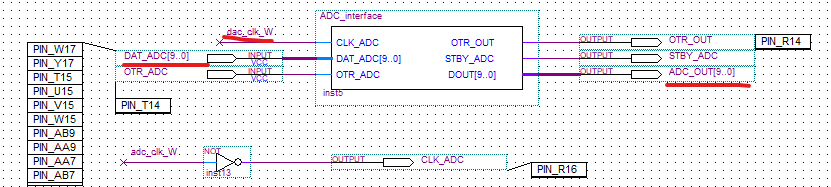
ADC module
module ADC_interface(
  CLK_ADC  ,   //  adc clk
  DAT_ADC  ,   //  input data, from adc
  OTR_ADC  ,   //  from adc , signal out of range flag
  OTR_OUT  ,   //  output otr flag
  STBY_ADC ,   //  adc stand by, set 0 make adc running
  DOUT     );   //  data out


input        CLK_ADC  ;
input  [9:0] DAT_ADC  ;
input        OTR_ADC  ;
output       OTR_OUT  ;
output       STBY_ADC ;

output [9:0] DOUT     ;


reg [9:0] DOUT   ;

reg       OTR_OUT;

always @ (posedge CLK_ADC) begin
  DOUT    <= DAT_ADC   ;
  OTR_OUT <= OTR_ADC;
end

assign STBY_ADC = 1'b0;

endmodule
Save, generate components, connect circuits, assign pins
(the place circled in the figure below indicates that the high 12 bits are given to the DAC and the low 4 bits are suspended)
Next, compile and download, and grab the data with signaltap
When the key is 011
 Observe with ADC clock
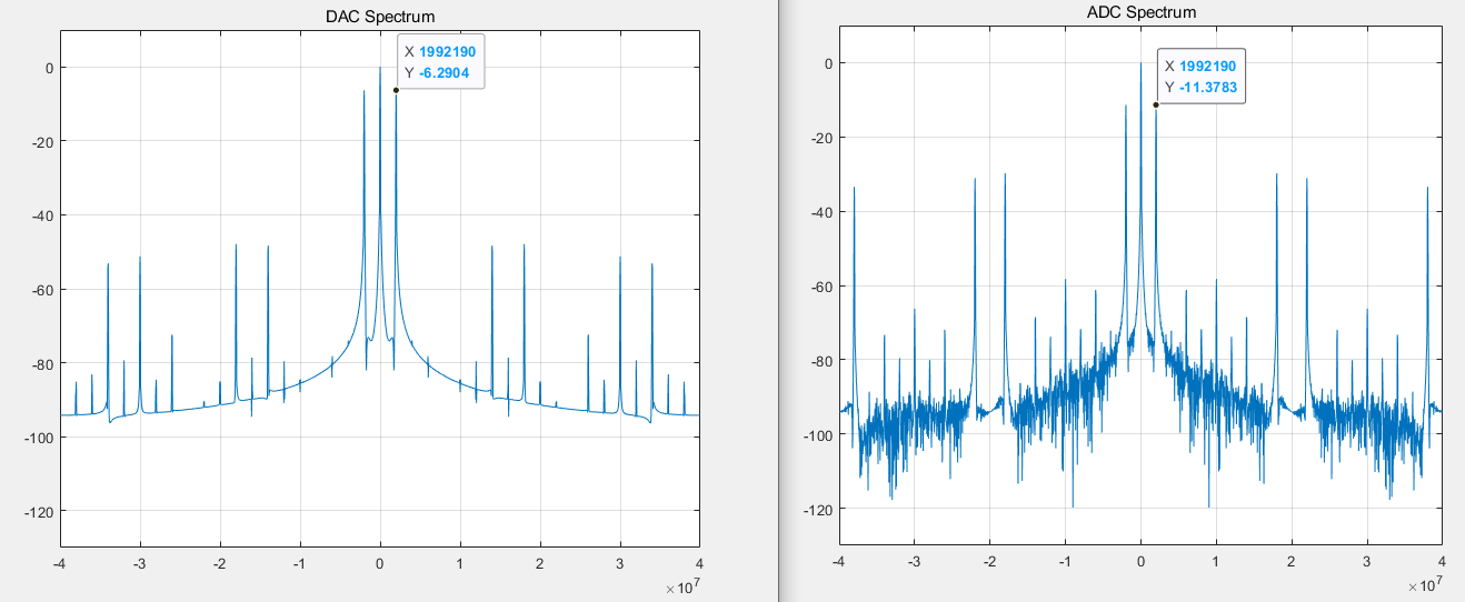
ADC spectrum is observed with ADC clock, and the frequency is 2M
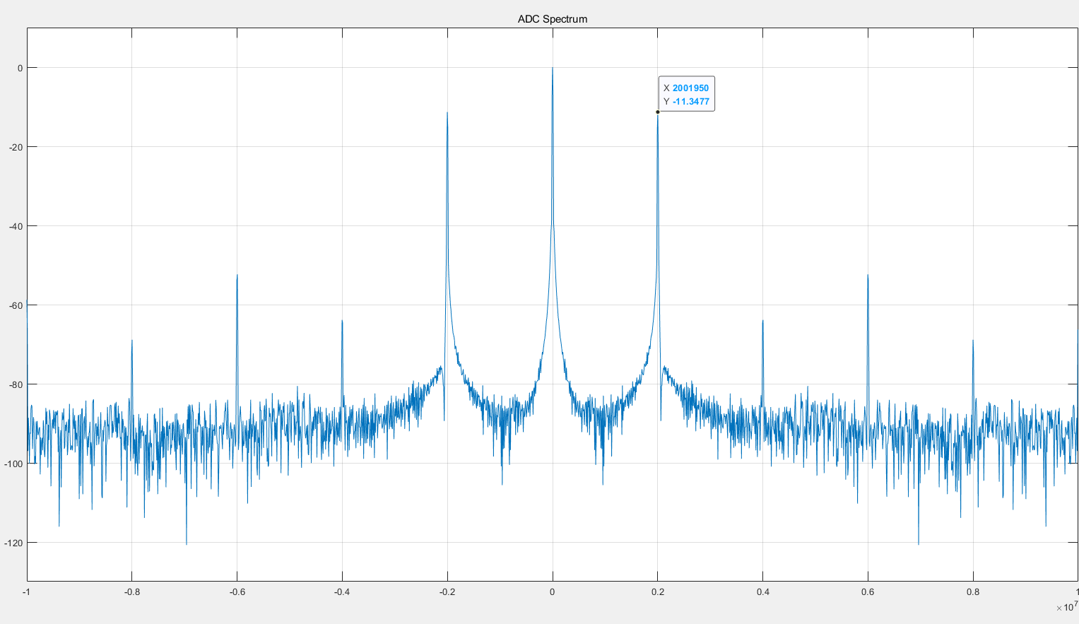
The DAC spectrum is observed based on the DAC clock, and the frequency also reaches the required 2M
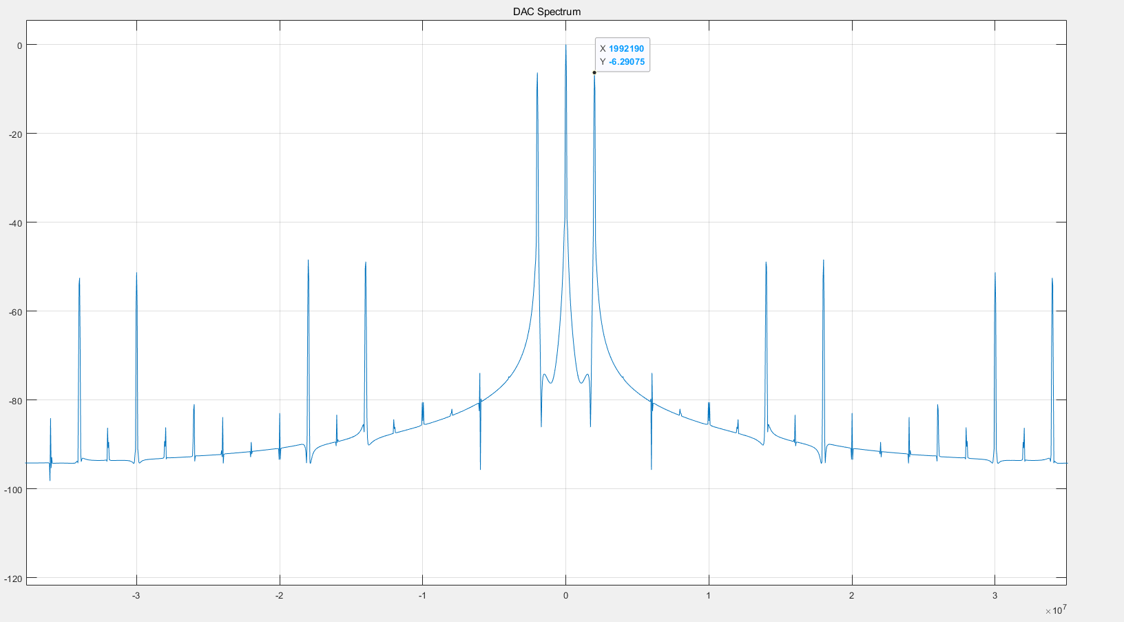
Connect to the oscilloscope and observe the frequency. The result is correct and 2M
The spectral gain of other clutter is lower than 60dB, and the spectral purity is relatively good
Thinking questions

Visible, dat_ At ADC is the 20M data stream of ADC, which can be processed by connecting 80M clock
Connect the 80M DAC clock to the ADC clock,
It can be found that when the sampling clock frequency is higher, the envelope of Sa function is more obvious. However, the spectral purity of ADC is not very high. Filters can be added to filter out clutter