Huada HC32f460 startup analysis and clock configuration
Statement: the personal experience written due to learning may be wrong due to limited ability
software environment
- System: win10
- sdk version: hc32f460_ ddl_ Rev2. zero
- Data manual version: HC32F460 series user manual Rev1 21.pdf
- ide: keil5
- Development board: official evaluation board (EVB-HC32F460)
- Time: July 1, 2021
1. Start up process
1.1 step 1: read the content on the area address 0x400
The data book reads as follows:
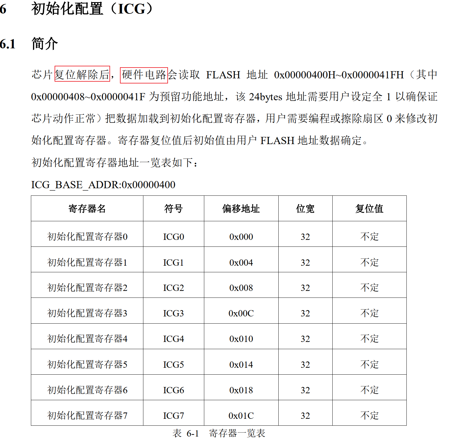
We should pay attention to two places:
-
Execute after the reset is released, which shows that the 0x400 address of reading flash is better than the program, that is, it should be executed before the program starts.
-
It is read by the hardware circuit, which shows that the reading position is not controlled by the legal person, that is 0x400. We can only write the information to the starting position of 0x400 when downloading the program.
This 0x400 is configured with very useful things, among which there is a watchdog. In fact, the watchdog of stm32 has always had a defect, that is, if a flight occurs between the chip startup and the execution of the main function, the program will not be able to restart and crash. hc32 avoids this problem and can be directly equipped with a watchdog when the reset is released, The stability of the system is improved. For other functions, please refer to the user manual.
1.2 step 2: reset and system clock configuration
This code is executed in assembly, that is s file, which is the same as the traditional cortex-m chip, performs reset_handler, configure the system clock systeninit, and execute__ Main, and finally jump to the user function main, because, like the traditional stm32, this is not discussed in detail.
-
It should be noted that this configuration system clock systeninit often uses the internal high-speed clock of the chip. This configuration system clock function is provided by the sdk. It is not recommended to directly modify it to the external clock in this step (do not modify the things of the sdk at will). Therefore, it is necessary to reconfigure it to the external high-speed clock when executing the user program.
-
At the same time, it should be noted that during the execution of the systeninit function for configuring the system clock and the previous period, because there is no clock configuration, it is driven by the internal high-speed clock direct connection, so the execution of that program is very slow.
-
In this s file, it may be strange to see those interrupt numbers. When people come from stm32, they will have an illusion and write the interrupt number as serial number irq001_ What is the purpose of handler and 002? This is because the interrupt of Huada is very flexible. When the program configures the interrupt, it needs to bind an interrupt number and a callback function for an interrupt event. This is to solve the problem of judging the incoming interrupt: for example, in stm32, when we open the serial port to receive and send interrupts at the same time, At this time, two interrupts will enter an interrupt function, and then add if to this interrupt function to judge whether the interrupt of the serial port has occurred. Huada can bind each event with an interrupt number, so that the serial port will receive the interrupt and send the interrupt into a different interrupt function.
1.3 step 3: enter the main function of the user program
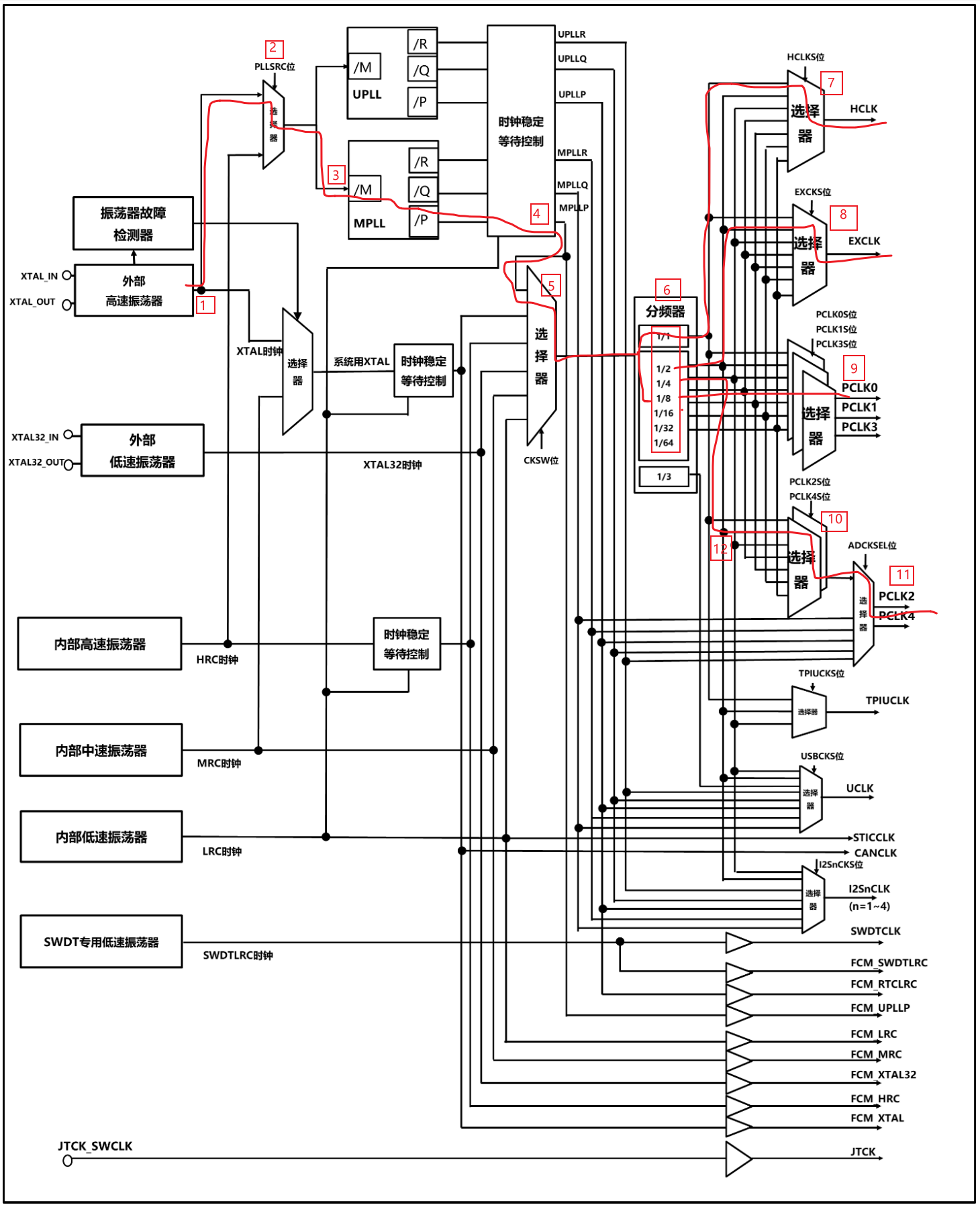
Entering the main function means entering the user's own program. At this time, it is necessary to reconfigure the clock first, because the internal high-speed clock is often inaccurate and vulnerable to interference. The configuration function needs to be written according to the clock system block diagram of mcu. Thank you for writing a clock configuration function void BSP in the official evaluation board (EVB-HC32F460) software package provided on the official website_ CLK_ Init (void), compared with the ready-made changes, is much easier. Let's compare this function with the clock system block diagram.
2. User clock configuration analysis
In the official evaluation board (EVB-HC32F460) software package provided on the official website, ev_hc32f460_lqfp100_v2.c file provides a method function to configure the external high-speed crystal oscillator to 200MHZ. Next, we will compare and analyze the configuration process. The clock configuration program is as follows:
//Huada initialization clock is 200MHZ
void BSP_CLK_Init(void)
{
    stc_clk_sysclk_cfg_t    stcSysClkCfg;
    stc_clk_xtal_cfg_t      stcXtalCfg;
    stc_clk_mpll_cfg_t      stcMpllCfg;
    stc_sram_config_t       stcSramConfig;

    MEM_ZERO_STRUCT(stcSysClkCfg);
    MEM_ZERO_STRUCT(stcXtalCfg);
    MEM_ZERO_STRUCT(stcMpllCfg);
    MEM_ZERO_STRUCT(stcSramConfig);

    /* Set bus clk div. */
    stcSysClkCfg.enHclkDiv  = ClkSysclkDiv1; //The clock of hclk comes from the frequency divider 1
    stcSysClkCfg.enExclkDiv = ClkSysclkDiv2; //exclk clock comes from frequency divider 2
    stcSysClkCfg.enPclk0Div = ClkSysclkDiv1; //The clock of Pclk0 comes from the frequency division 1 of the frequency divider
    stcSysClkCfg.enPclk1Div = ClkSysclkDiv2; //The clock of Pclk1 comes from the frequency division 2 of the frequency divider
    stcSysClkCfg.enPclk2Div = ClkSysclkDiv4; //The clock of Pclk2 comes from the frequency divider 4
    stcSysClkCfg.enPclk3Div = ClkSysclkDiv4; //The clock of Pclk3 comes from the frequency divider 4
    stcSysClkCfg.enPclk4Div = ClkSysclkDiv2; //The clock of Pclk4 comes from the frequency divider 2
    CLK_SysClkConfig(&stcSysClkCfg);

    /* Config Xtal and Enable Xtal */
    stcXtalCfg.enMode = ClkXtalModeOsc;
    stcXtalCfg.enDrv = ClkXtalLowDrv;
    stcXtalCfg.enFastStartup = Enable;
    CLK_XtalConfig(&stcXtalCfg);
    CLK_XtalCmd(Enable);

    /* sram init include read/write wait cycle setting */
    stcSramConfig.u8SramIdx = Sram12Idx | Sram3Idx | SramHsIdx | SramRetIdx;
    stcSramConfig.enSramRC = SramCycle2;
    stcSramConfig.enSramWC = SramCycle2;
    SRAM_Init(&stcSramConfig);

    /* flash read wait cycle setting */
    EFM_Unlock();
    EFM_SetLatency(EFM_LATENCY_5);
    EFM_Lock();

    /* MPLL config (XTAL / pllmDiv * plln / PllpDiv = 200M). */
    stcMpllCfg.pllmDiv = 1ul;
    stcMpllCfg.plln    = 50ul;
    stcMpllCfg.PllpDiv = 2ul;
    stcMpllCfg.PllqDiv = 2ul;
    stcMpllCfg.PllrDiv = 2ul;
    CLK_SetPllSource(ClkPllSrcXTAL);//Turn on the external high-speed crystal oscillator
    CLK_MpllConfig(&stcMpllCfg); //Configure MPLL

    /* Enable MPLL. */
    CLK_MpllCmd(Enable);//Open MPLL
    /* Wait MPLL ready. */
    while(Set != CLK_GetFlagStatus(ClkFlagMPLLRdy))
    {
        ;
    }
    /* Switch driver ability */
    PWC_HS2HP();
    /* Switch system clock source to MPLL. */
    CLK_SetSysClkSource(CLKSysSrcMPLL);
}
First of all, we all need to know that the configuration principle of the clock should be from the back to the front, that is, from the peripheral to the crystal oscillator. Let's compare the clock system block diagram to analyze the above code.
The configuration direction of the clock system block diagram of the above function comparison is as follows: