Recording IC Test & verification practice 2020.11.13 - 2021.1.22
Although it's been a long time hhh, I feel that I can sort out what I learned in my senior internship. The internship part is divided into two parts: Test (7 days to move bricks) & verification part (free study for more than 1 month)
1. Chip test (formed chip)
1.1 task 1 bist communication test + voltage / temperature test
1.2 calculate PLL output frequency
2. Chip verification
2.1 task 1: Learn Verilog
2.2 task 2: learn Linux System vi/vim
2.3 task 3: read and write registers through JTAG, read and write registers through AHB bus, check the simulation waveform, and find errors and omissions in the design register.
3.Verilog designs a register
3.1 understand a Verilog code similar to L1 register
3.2 design a cache L2 register
1. Chip test (formed chip)
Overview: bist communication test + voltage / temperature test
1.1 task 1: read and write the difinfo register through the external interface, control the REQCR / REQSR register to trigger the bus bridge to initiate AHB request ----- read and write the bist register to complete the bist communication test, and judge whether the communication test is successful by reading the returned data.
It mainly controls the bist behavior of RAM and checks the bist results by reading and writing the bist csr register;
1) Know how to calculate the address of the target register;
Base address + offset address;
Base address: Chip Design Manual
Offset address: the description of each register in the chip design manual is the offset address
2) Know how to read and write the target register;
If it is a write operation, the process is roughly as follows:
1) Input the "write difinfo register" command through the external interface and input the write operation data;
2) Input the "write REQCR register" command through the external interface, input the length information of the write operation, and indicate that it is a write operation at the same time;
3) Input the "write REQAR register" command through the external interface, input the starting address of the write operation, and trigger the bus bridge to initiate the AHB request.
If it is a read operation, the process is roughly as follows:
1) Input the "write REQCR register" command through the external interface, input the length information of the read operation, and indicate that it is a read operation;
2) Input the "write REQAR register" command through the external interface, input the starting address of the read operation, and trigger the bus bridge to initiate the AHB request;
3) Input the "read DOFIFO register" command through the external interface to get the data returned by the read operation.
1.2 task 2: calculate the output frequency of PLL (phase locked loop) and adjust the dial switch appropriately
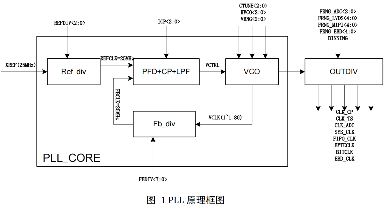
PD: phase detector - phase comparison, which completes the phase comparison between the input signal and the feedback signal. The output voltage is proportional to the phase difference between the two input voltages
(PFD: frequency and phase discriminator - system accuracy and stability CP: charge pump - wide frequency capture range and fast locking capability LPF: low-pass filter - smooth filtering)
LF: loop filter – filter out the high-frequency part of the voltage generated by the phase detector and smooth the filtering effect
VCO: voltage controlled oscillator – oscillation frequency generated by controlled voltage source
1. The output of the VCO is collected and frequency divided;
2. And the reference signal are input to the phase discriminator at the same time;
3. The phase discriminator outputs a DC pulse voltage by comparing the frequency difference between the two signals;
4. Control the VCO to change its frequency;
5. In this way, after a very short time, the output of VCO will stabilize at a certain expected value.
Note: this chip Xref=25M first passes through R frequency division, outputs 25M to PFD+CP+LPF, transmits it to VCO, transmits it to Fb frequency division inside the PLL, and transmits it to out frequency division outside to generate different frequencies and transmit it to the clock
2. Chip verification
2.1 task 1: Learn Verilog, grammar and advanced practice. I will write it in detail in my next blog
2.2 task 2: learn Linux System vi/vim, check waveforms, etc. I have uploaded resources Linux common commands and vim common commands
2.3 task 3: read and write registers through JTAG interface, read and write registers through AHB bus, check the simulation waveform, and find errors and omissions in the design register. ( rfuse_test; tfuse_test; reg_rfuse_test; reg_tfuse_test; bist_test; )
The code idea is: write 1 on the determined register address, and check whether the register writes 1 successfully, whether the address of write 1 is correct, and whether write 1 meets the conditions of register setting by checking the position of 1 and whether the write 1 operation is completed. The code snippet is as follows:
Insert the code slice here
task   rfuse_test;
begin

    req_tbox_reg_wad(1'b1,13'h04,      32'h12);  // CMR
    $display("---------redundance efuse test-----------");
    for(K=0;K<8;K=K+1)begin
	    $display("---------Bank-%x-----------",K);
        nn=32'h01;
        for(N=0;N<32;N=N+1)begin
            wait(ef_access_fsm[5:0]==6'h03);
        //    $display("ef_access_fsm==0x03",$time);
            #20;
     //       $display("---------nn==-%x-----------",nn);
            req_ef_red_wbad (1'b1, K[2:0],K[7:0],nn[31:0]);
            #2000;
            wait(ef_access_fsm[5:0]==6'h03);
       //     $display("ef_access_fsm==0x03",$time);
            req_ef_red_wbad (1'b0, K[2:0],K[7:0],32'h00);
            nn=nn<<1;
        end
    end
    $display("---------test-----------");
    for(K=0;K<8;K=K+1)begin
	    $display("-------KKK=%x---------",K);
      //  for(N=0;N<32;N=N+1)begin
            req_ef_red_wbad (1'b0, K[2:0],K[7:0],32'h00);
    //    end
    end

end
endtask

task   bist_test;
begin
$display("# Bist Test Start.........",$time);
force tb_chip.u_ddr4_chip.u_ddr4_core.u_mram_wrap.DIN_DL=64'h1;
tb_chip.u_ddr4_chip.u_ddr4_core.u_efuse_wrap.u_tbox.u_ctrl_reg.GP_BIST_enable=1'b1;
wait(tb_chip.u_ddr4_chip.u_ddr4_core.u_efuse_wrap.u_tbox.u_ctrl_reg.bist_done);
#2000;
//-----------w-----A------D---
req_reg_wad(1'b0,16'h8015,32'h00);
req_reg_wad(1'b0,16'h8006,32'h00);
req_reg_wad(1'b0,16'h8007,32'h00);
req_reg_wad(1'b0,16'h8008,32'h00);
req_reg_wad(1'b0,16'h800a,32'h00);

end
endtask
3.Verilog designs a register
3.1 understand a Verilog code similar to L1 register
Occupy the pit first and do it again tomorrow
3.2 design a cache L2 register