Because our company needs to develop burning tools, I finally realized this function by searching relevant documents through google and looking at the technical documents of ARM company. I dare to confidently say that the SWD theory is the most easy to understand.
As an ARM embedded engineer, you should know how to download the debugger, but do you really know how to download and Debug SWD? What physical interface and how the ARM chip is connected depends entirely on the architecture of the chip Debug subsystem?
You can get DAP(Debug Access Port) information from the Debug section of the chip manual. I debugged the chip of S32K3 series, the latest on-board chip of NXP company. I learned from the Debug subsystem chapter of S32K3xx Reference Manual that the Debug and Trace interfaces of the chip are based on the Arm CoreSight SoC-400 standard. From Arm CoreSight SoC-400 Technical Reference Manual You can get detailed information in the chapter Debug Access Port. Only the key contents are introduced here, and only the parts involved are introduced.
Reference documents: Arm CoreSight SoC-400 Technical Reference Manual , CoreSight Components Technical Reference Manual , Arm CoreSight Architecture Specification.
from Arm CoreSight SoC-400 Technical Reference Manual Figure 4-1 Structure of the CoreSight SoC-400 DAP components shows that SWD is only a way to access the chip debugging subsystem.
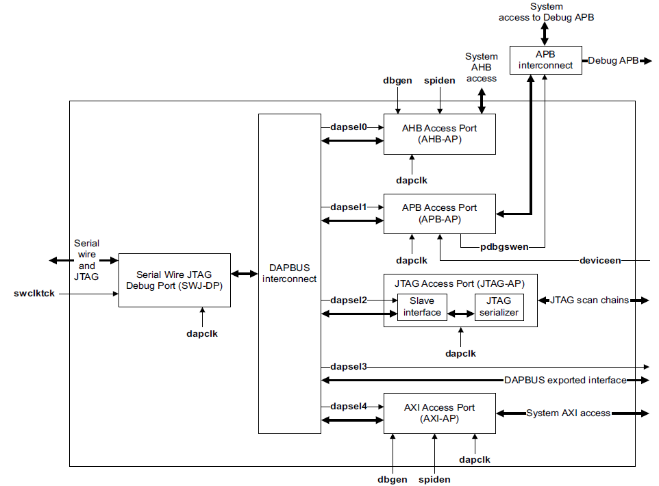
So how does the external debugging tool access to the ARM core through SWD? Let's introduce the CoreSight SoC-400 DAP component architecture in detail.
DAP is a collection of SOC components accessed by off chip debugging tools. The access method is based on ARM ® Debugging interface architecture specification ADIv5.0~ADIv5.2 realization.
The DAP consists of the following components:
• DP is used to manage connections to external debuggers.
• AP accesses system on chip resources. There can be multiple APS of each type.
• DAPBUS interconnection for connecting DP to one or more AP S.
AP provides non intrusive access:
• download or burn models with CoreSight components. It is usually completed through system level CoreSight APB bus and APB-AP.
• memory mapped system components, usually AXI-AP or AHB-AP.
• debug components configured using legacy JTAG of JTAG-AP.
Moreover, some processors that support CoreSight are directly connected to the DAPBUS interconnect and implement their own ADIv5 compatible AP.
The CoreSight SoC has a single multifunctional DP as follows:
SWJ-DP # this is a combined debugging port, which can be through adiv5 1 defined JTAG or serial line protocol. It contains two debug ports SW-DP and JTAG-DP. You can select them through the interface timing command to switch between debug port interfaces.
JTAG-DP} is compatible with DP architecture version 0. SW-DP is compatible with DP architecture version 2 and Serial Wire protocol version 2, so that SW-DP can share connection with other SW-DP or other implementation components.
The AP ports included in the CoreSight SoC are:
AXI-AP AXI-ap implements the ADIv5 storage access port (MEM-AP) architecture to connect directly to the AXI storage system. You can connect it to other memory systems using appropriate bridging components.
AHB-AP - AHB-AP provides an AHB Lite master station for accessing the system AHB bus. This is compatible with adiv5 1 and can perform 8 to 32-bit access.
APB-AP # APB-AP in AMBA v3 0 provides an APB master device for accessing and debugging the APB bus. This is compatible with the MEM-AP architecture with a 32-bit fixed transfer size.
JTAG-AP jtag-ap provides JTAG access to on-chip components and serves as the JTAG main port to drive the JTAG chain in the ASIC. This is adiv5 Implementation of JTAG-AP in 1.
DAPBUS} interconnect connects DP to AP. The system may not contain some types of APS, or may contain multiple APS of the same type.
If you simply look at the CoreSight SoC-400 DAP component architecture, it will feel empty. Let's take a look at it in combination with the S32K3XX DAP architecture diagram.
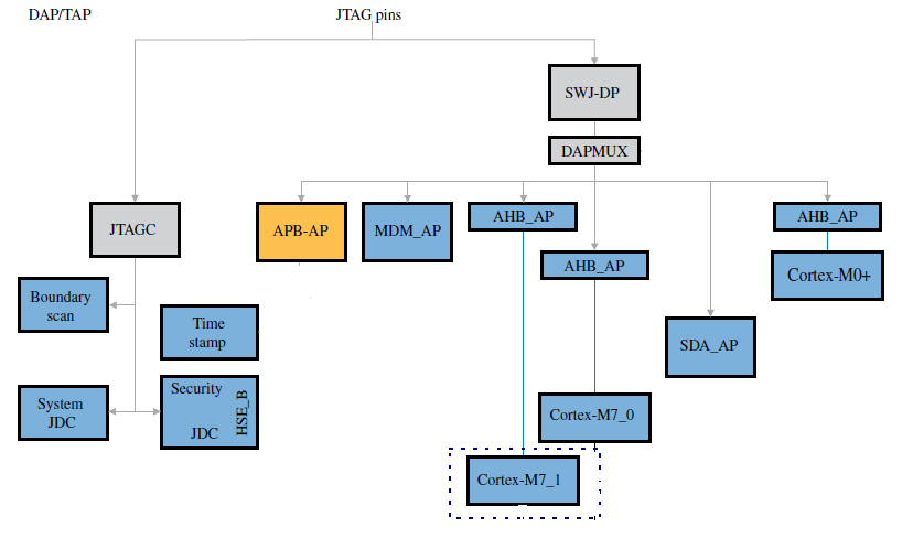
From the DAP architecture of the chip, it is not difficult to see that the S32K3 adopts Arm ® CoreSight ™ framework.
You can basically find the DAP architecture correspondence between CoreSight SoC-400 and S32K3XX:
S32K3XX CoreSight SoC-400
SWJ-DAP <--> Serial Wire JTAG Debug Port (SWJ-DP)
DAPMUX <--> DAPBUS interconnect
AHB_AP <--> AHB Access Port (AHB-AP)
APB-AP <--> APB Access Port (APB-AP)
MDM_AP <--> DAPBUS exported interface
SDA_AP <--> DAPBUS exported interface
SWJ-DP consists of JTAG-DP and SW-DP. It selects JTAG or SWD as the connection mechanism and enables JTAG-DP or SW-DP as the interface of DAP.
JTAG and SWD interfaces
The JTAG interface has four forcing pins tck, tms, tdi and tdo, and an optional reset pin ntrst. JTAG-DP and SW-DP also need independent power on reset npotrst.
The SWD interface requires two pins:
• bidirectional swdio signal.
• clock swclk, which can be input or output from the device.
In order for JTAG or SWD to share the connector, it must be connected outside the SWJ-DP module. In particular, tms must be bidirectional pin to support bidirectional swdio pin in SWD mode.
20-Pin ARM Standard JTAG Connector
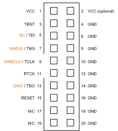
(From https://www2.keil.com/coresight/coresight-connectors)
It supports JTAG interfaces for accessing ARM7 and ARM9 based devices. For cortex MX devices, it supports serial lines and JTAG interfaces to access all SWD, SWV and JTAG signals available on cortex MX devices.
How do debugging tools access cortex MX?
Reference documents: ARM® Debug Interface Architecture Specification ADIv5.0 to ADIv5.2
DAP access mode is based on ARM ® Debugging interface architecture specification adiv5 0~ADIv5. 2 implementation.
The structure block diagram of DAP * * * * is as follows:
come from ARM® Debug Interface Architecture Specification ADIv5.0 to ADIv5.2 Figure A1-2 Structure of the DAP, showing DPv0 JTAG-DP accesses to a generic AP
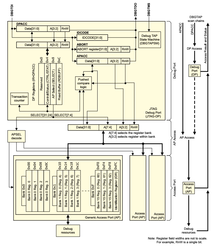
ADI includes:
Debug Access Port (DAP), external physical connection of DAP and connection between DAP and internal debugging resource components.
DAP contains two logic modules, Debug Port(DP) and Access Port(AP). DP to connect the external host and AP to access the internal debug component register:
• Access to the Debug Port (DP) registers. This is provided by Debug Port accesses (DPACC).
• Access to the Access Port (AP) registers. This is provided by Access Port accesses (APACC)
ADIv5 standard external interface supports the following DP:
• The JTAG Debug Port (JTAG-DP)
• The Serial Wire Debug Port (SW-DP)
• The Serial Wire/JTAG Debug Port (SWJ-DP)
Internal resource interfaces include:
AP (MEM-AP or JTAG-AP)
Since I choose to use the SW-DP method for access, I will only introduce the SWD protocol processing flow here.
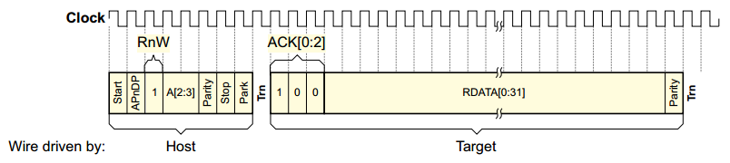
Let's analyze the format of SW-DP message below (in case of translation error, use the original English text):
Start A single start bit, with value 0b1.
APnDP A single bit, indicating whether the Debug Port or the Access Port Access register is to be accessed. This bit is 0b0 for a DPACC access, or 0b1 for an APACC access.
RnW A single bit, indicating whether the access is a read or a write. This bit is 0b0 for a write access, or 0b1 for a read access.
A[2:3] Two bits, giving the A[3:2] address field for the DP or AP register Address:
• For a DPACC access, the register being addressed depends on the A[3:2] value and, if A[3:2]==0b01, the value that is held in SELECT. DPBANKSEL. For details, see:
— DP architecture version 1 (DPv1) address map on page B2-50
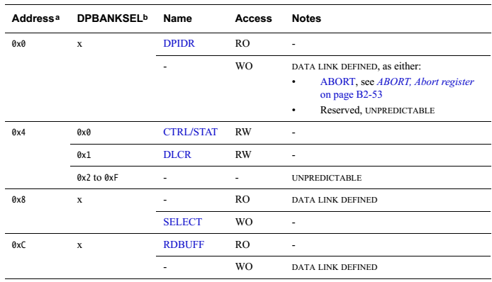
— DP architecture version 2 (DPv2) address map on page B2-51.
• For an APACC access, the register being addressed depends on the A[3:2] value and the value
that is held in SELECT.{APSEL,APBANKSEL}. For details about addressing, see:
— MEM-AP Programmers' Model on page C2-169 for accesses to a MEM-AP register
— JTAG-AP register summary on page C3-206 for accesses to a JTAG-AP register.
Note
The A[3:2] value is transmitted Least Significant Bit (LSB) first on the wire, which is why it appears as A[2:3] on the diagrams.
Parity A single parity bit for the preceding packet. See Parity on page B4-108.
Stop A single stop bit. In the synchronous SWD protocol, this bit is always 0b0.
Park A single bit. The host must drive the Park bit HIGH to park the line before tristating it for the turnaround period, to ensure that the line is read as HIGH by the target, which is required because the pull-up on the SWD interface is weak. The target reads this bit as 0b1.
Trn Turnaround. See Line turnaround on page B4-107.
Note
All the examples that are given in this chapter show the default turnaround period of one cycle.
ACK[0:2] A three-bit target-to-host response.
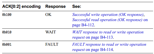
WDATA[0:31]
32 bits of write data, from host to target.
RDATA[0:31]
32 bits of read data, from target to host
We have understood the message format, so we can understand it in combination with the message reading and writing sequence diagram of SWD.
Successful write operation (OK response)
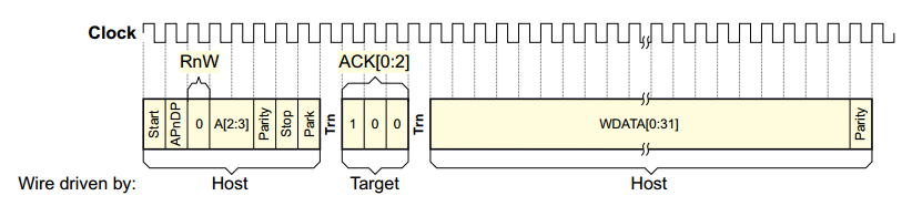
Successful read operation (OK response)
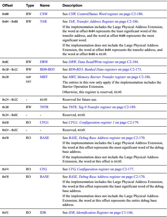
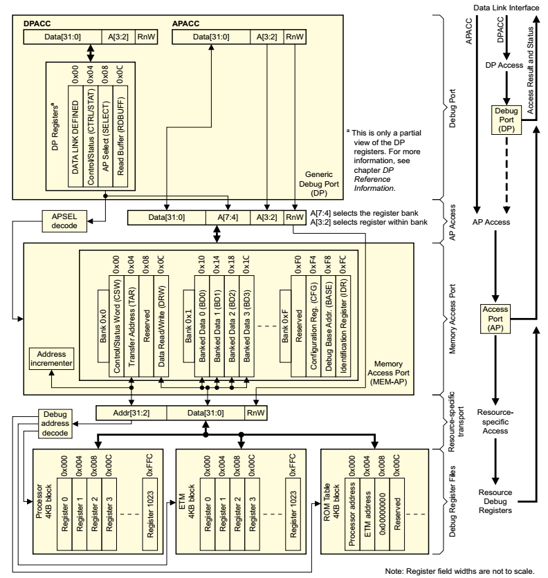
Next, I will combine the Successful write operation (OK response) and Structure of the Debug Access Port as an example to demonstrate how SWD controls DAP.
Every AP or DP access transaction from the debugger includes two address bits, A[3:2]:
• For a DP register access, the address bits A[3:2] and SELECT.DPBANKSEL determine which register is accessed. SELECT is a DP register.
• For an AP register access, SELECT.APSEL selects an AP to access, and the address bits A[3:2] are combined with SELECT.APBANKSEL to determine which AP register is accessed, as summarized in Structure of the Debug Access Port. That is, the two address bits A[3:2] are decoded to select one of the four 32-bit words from the register bank indicated by SELECT.APBANKSEL in the AP indicated by SELECT.APSEL. Bits [1:0] of all AP and DP register addresses are 0b00.
If I want to write 0xF0000001 to AP0 register 0x14, the operation flow of the debugging tool is as follows:
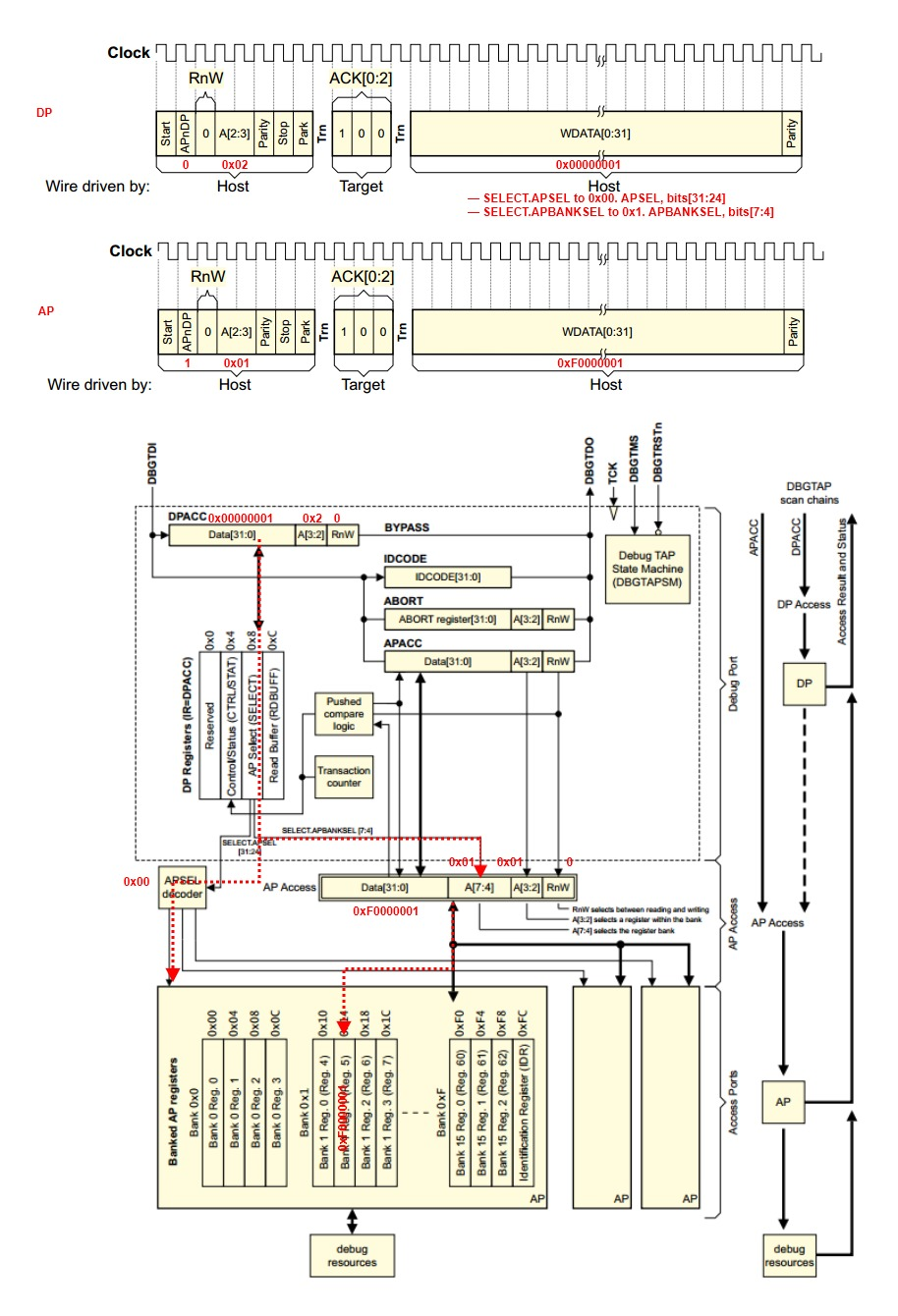
Use the DP register to write to the SELECT register of DP:
— SELECT.APSEL to 0x00. APSEL, bits[31:24]
— SELECT.APBANKSEL to 0x1. APBANKSEL, bits[7:4]
APnDP write 0 indicates DP operation, and A[3:2] write 0x02 indicates operation 0x08} SELECT register. Write 0x00000001
Use AP register to write to 0x14 register of AP0:
APnDP write 1 indicates AP operation. Since apbankselect has been selected for DP SELECT, A[3:2] write 0x01 indicates operation 0x14 register. Write 0xF0000001 In this case, four registers such as 0x10~0x1C can be accessed.
Other AP operations are actually the same.
Let me know a little about MEM-AP
From ARM® Debug Interface Architecture Specification ADIv5.0 to ADIv5.2 Figure C2-1 MEM AP connecting the DP to debug components
To put it bluntly, MEM-AP provides DAP with a direct access to the system address space. The operation is actually the same as the access of general AP. MEM-AP accesses the system address space. In fact, there is an additional layer of indirect access. We look at the whole process directly from the OpenOCD source code.
https://sourceforge.net/p/openocd/code/ci/v0.11.0/tree/src/target/cortex_m.c#l2521
struct target_type cortexm_target = {
	.name = "cortex_m",
	.deprecated_name = "cortex_m3",

	.poll = cortex_m_poll,
	.arch_state = armv7m_arch_state,

	.target_request_data = cortex_m_target_request_data,

	.halt = cortex_m_halt,
	.resume = cortex_m_resume,
	.step = cortex_m_step,

	.assert_reset = cortex_m_assert_reset,
	.deassert_reset = cortex_m_deassert_reset,
	.soft_reset_halt = cortex_m_soft_reset_halt,

	.get_gdb_arch = arm_get_gdb_arch,
	.get_gdb_reg_list = armv7m_get_gdb_reg_list,

	.read_memory = cortex_m_read_memory,
	.write_memory = cortex_m_write_memory,
	.checksum_memory = armv7m_checksum_memory,
	.blank_check_memory = armv7m_blank_check_memory,

	.run_algorithm = armv7m_run_algorithm,
	.start_algorithm = armv7m_start_algorithm,
	.wait_algorithm = armv7m_wait_algorithm,

	.add_breakpoint = cortex_m_add_breakpoint,
	.remove_breakpoint = cortex_m_remove_breakpoint,
	.add_watchpoint = cortex_m_add_watchpoint,
	.remove_watchpoint = cortex_m_remove_watchpoint,

	.commands = cortex_m_command_handlers,
	.target_create = cortex_m_target_create,
	.target_jim_configure = adiv5_jim_configure,
	.init_target = cortex_m_init_target,
	.examine = cortex_m_examine,
	.deinit_target = cortex_m_deinit_target,

	.profiling = cortex_m_profiling,
};
OpenOCD realizes the access of Cortex M system address space through the access of DAP MEM AP.
cortex_m_read_memory and cortex_m_write_memory implements read and write operations. Let's see how these two functions are implemented.
cortex_m_read_memory implementation
static int cortex_m_read_memory(struct target *target, target_addr_t address,
	uint32_t size, uint32_t count, uint8_t *buffer)
{
	struct armv7m_common *armv7m = target_to_armv7m(target);

	if (armv7m->arm.is_armv6m) {
		/* armv6m does not handle unaligned memory access */
		if (((size == 4) && (address & 0x3u)) || ((size == 2) && (address & 0x1u)))
			return ERROR_TARGET_UNALIGNED_ACCESS;
	}

	return mem_ap_read_buf(armv7m->debug_ap, buffer, size, count, address);
}

int mem_ap_read_buf(struct adiv5_ap *ap,
		uint8_t *buffer, uint32_t size, uint32_t count, uint32_t address)
{
	return mem_ap_read(ap, buffer, size, count, address, true);
}

/**
 * Synchronous read of a block of memory, using a specific access size.
 *
 * @param ap The MEM-AP to access.
 * @param buffer The data buffer to receive the data. No particular alignment is assumed.
 * @param size Which access size to use, in bytes. 1, 2 or 4.
 * @param count The number of reads to do (in size units, not bytes).
 * @param adr Address to be read; it must be readable by the currently selected MEM-AP.
 * @param addrinc Whether the target address should be increased after each read or not. This
 *  should normally be true, except when reading from e.g. a FIFO.
 * @return ERROR_OK on success, otherwise an error code.
 */
static int mem_ap_read(struct adiv5_ap *ap, uint8_t *buffer, uint32_t size, uint32_t count,
		uint32_t adr, bool addrinc)
{
	struct adiv5_dap *dap = ap->dap;
	size_t nbytes = size * count;
	const uint32_t csw_addrincr = addrinc ? CSW_ADDRINC_SINGLE : CSW_ADDRINC_OFF;
	uint32_t csw_size;
	uint32_t address = adr;
	int retval = ERROR_OK;

	/* TI BE-32 Quirks mode:
	 * Reads on big-endian TMS570 behave strangely differently than writes.
	 * They read from the physical address requested, but with DRW byte-reversed.
	 * For example, a byte read from address 0 will place the result in the high bytes of DRW.
	 * Also, packed 8-bit and 16-bit transfers seem to sometimes return garbage in some bytes,
	 * so avoid them. */

	if (size == 4)
		csw_size = CSW_32BIT;
	else if (size == 2)
		csw_size = CSW_16BIT;
	else if (size == 1)
		csw_size = CSW_8BIT;
	else
		return ERROR_TARGET_UNALIGNED_ACCESS;

	if (ap->unaligned_access_bad && (adr % size != 0))
		return ERROR_TARGET_UNALIGNED_ACCESS;

	/* Allocate buffer to hold the sequence of DRW reads that will be made. This is a significant
	 * over-allocation if packed transfers are going to be used, but determining the real need at
	 * this point would be messy. */
	uint32_t *read_buf = calloc(count, sizeof(uint32_t));
	/* Multiplication count * sizeof(uint32_t) may overflow, calloc() is safe */
	uint32_t *read_ptr = read_buf;
	if (read_buf == NULL) {
		LOG_ERROR("Failed to allocate read buffer");
		return ERROR_FAIL;
	}

	/* Queue up all reads. Each read will store the entire DRW word in the read buffer. How many
	 * useful bytes it contains, and their location in the word, depends on the type of transfer
	 * and alignment. */
	while (nbytes > 0) {
		uint32_t this_size = size;

		/* Select packed transfer if possible */
		if (addrinc && ap->packed_transfers && nbytes >= 4
				&& max_tar_block_size(ap->tar_autoincr_block, address) >= 4) {
			this_size = 4;
			retval = mem_ap_setup_csw(ap, csw_size | CSW_ADDRINC_PACKED);
		} else {
			retval = mem_ap_setup_csw(ap, csw_size | csw_addrincr);
		}
		if (retval != ERROR_OK)
			break;

		retval = mem_ap_setup_tar(ap, address);
		if (retval != ERROR_OK)
			break;

		retval = dap_queue_ap_read(ap, MEM_AP_REG_DRW, read_ptr++);
		if (retval != ERROR_OK)
			break;

		nbytes -= this_size;
		if (addrinc)
			address += this_size;

		mem_ap_update_tar_cache(ap);
	}

	if (retval == ERROR_OK)
		retval = dap_run(dap);

	/* Restore state */
	address = adr;
	nbytes = size * count;
	read_ptr = read_buf;

	/* If something failed, read TAR to find out how much data was successfully read, so we can
	 * at least give the caller what we have. */
	if (retval != ERROR_OK) {
		uint32_t tar;
		if (mem_ap_read_tar(ap, &tar) == ERROR_OK) {
			/* TAR is incremented after failed transfer on some devices (eg Cortex-M4) */
			LOG_ERROR("Failed to read memory at 0x%08"PRIx32, tar);
			if (nbytes > tar - address)
				nbytes = tar - address;
		} else {
			LOG_ERROR("Failed to read memory and, additionally, failed to find out where");
			nbytes = 0;
		}
	}

	/* Replay loop to populate caller's buffer from the correct word and byte lane */
	while (nbytes > 0) {
		uint32_t this_size = size;

		if (addrinc && ap->packed_transfers && nbytes >= 4
				&& max_tar_block_size(ap->tar_autoincr_block, address) >= 4) {
			this_size = 4;
		}

		if (dap->ti_be_32_quirks) {
			switch (this_size) {
			case 4:
				*buffer++ = *read_ptr >> 8 * (3 - (address++ & 3));
				*buffer++ = *read_ptr >> 8 * (3 - (address++ & 3));
				/* fallthrough */
			case 2:
				*buffer++ = *read_ptr >> 8 * (3 - (address++ & 3));
				/* fallthrough */
			case 1:
				*buffer++ = *read_ptr >> 8 * (3 - (address++ & 3));
			}
		} else {
			switch (this_size) {
			case 4:
				*buffer++ = *read_ptr >> 8 * (address++ & 3);
				*buffer++ = *read_ptr >> 8 * (address++ & 3);
				/* fallthrough */
			case 2:
				*buffer++ = *read_ptr >> 8 * (address++ & 3);
				/* fallthrough */
			case 1:
				*buffer++ = *read_ptr >> 8 * (address++ & 3);
			}
		}

		read_ptr++;
		nbytes -= this_size;
	}

	free(read_buf);
	return retval;
}
static int cortex_m_write_memory(struct target *target, target_addr_t address,
uint32_t size, uint32_t count, const uint8_t *buffer)
{
struct armv7m_common *armv7m = target_to_armv7m(target);
if (armv7m->arm.is_armv6m) {
/* armv6m does not handle unaligned memory access */
if (((size == 4) && (address & 0x3u)) || ((size == 2) && (address & 0x1u)))
return ERROR_TARGET_UNALIGNED_ACCESS;
}
return mem_ap_write_buf(armv7m->debug_ap, buffer, size, count, address);
}
int mem_ap_write_buf(struct adiv5_ap *ap,
const uint8_t *buffer, uint32_t size, uint32_t count, uint32_t address)
{
return mem_ap_write(ap, buffer, size, count, address, true);
}
/**
* Synchronous write of a block of memory, using a specific access size.
*
* @param ap The MEM-AP to access.
* @param buffer The data buffer to write. No particular alignment is assumed.
* @param size Which access size to use, in bytes. 1, 2 or 4.
* @param count The number of writes to do (in size units, not bytes).
* @param address Address to be written; it must be writable by the currently selected MEM-AP.
* @param addrinc Whether the target address should be increased for each write or not. This
* should normally be true, except when writing to e.g. a FIFO.
* @return ERROR_OK on success, otherwise an error code.
*/
static int mem_ap_write(struct adiv5_ap *ap, const uint8_t *buffer, uint32_t size, uint32_t count,
uint32_t address, bool addrinc)
{
struct adiv5_dap *dap = ap->dap;
size_t nbytes = size * count;
const uint32_t csw_addrincr = addrinc ? CSW_ADDRINC_SINGLE : CSW_ADDRINC_OFF;
uint32_t csw_size;
uint32_t addr_xor;
int retval = ERROR_OK;
/* TI BE-32 Quirks mode:
* Writes on big-endian TMS570 behave very strangely. Observed behavior:
* size write address bytes written in order
* 4 TAR ^ 0 (val >> 24), (val >> 16), (val >> 8), (val)
* 2 TAR ^ 2 (val >> 8), (val)
* 1 TAR ^ 3 (val)
* For example, if you attempt to write a single byte to address 0, the processor
* will actually write a byte to address 3.
*
* To make writes of size < 4 work as expected, we xor a value with the address before
* setting the TAP, and we set the TAP after every transfer rather then relying on
* address increment. */
if (size == 4) {
csw_size = CSW_32BIT;
addr_xor = 0;
} else if (size == 2) {
csw_size = CSW_16BIT;
addr_xor = dap->ti_be_32_quirks ? 2 : 0;
} else if (size == 1) {
csw_size = CSW_8BIT;
addr_xor = dap->ti_be_32_quirks ? 3 : 0;
} else {
return ERROR_TARGET_UNALIGNED_ACCESS;
}
if (ap->unaligned_access_bad && (address % size != 0))
return ERROR_TARGET_UNALIGNED_ACCESS;
while (nbytes > 0) {
uint32_t this_size = size;
/* Select packed transfer if possible */
if (addrinc && ap->packed_transfers && nbytes >= 4
&& max_tar_block_size(ap->tar_autoincr_block, address) >= 4) {
this_size = 4;
retval = mem_ap_setup_csw(ap, csw_size | CSW_ADDRINC_PACKED);
} else {
retval = mem_ap_setup_csw(ap, csw_size | csw_addrincr);
}
if (retval != ERROR_OK)
break;
retval = mem_ap_setup_tar(ap, address ^ addr_xor);
if (retval != ERROR_OK)
return retval;
/* How many source bytes each transfer will consume, and their location in the DRW,
* depends on the type of transfer and alignment. See ARM document IHI0031C. */
uint32_t outvalue = 0;
uint32_t drw_byte_idx = address;
if (dap->ti_be_32_quirks) {
switch (this_size) {
case 4:
outvalue |= (uint32_t)*buffer++ << 8 * (3 ^ (drw_byte_idx++ & 3) ^ addr_xor);
outvalue |= (uint32_t)*buffer++ << 8 * (3 ^ (drw_byte_idx++ & 3) ^ addr_xor);
outvalue |= (uint32_t)*buffer++ << 8 * (3 ^ (drw_byte_idx++ & 3) ^ addr_xor);
outvalue |= (uint32_t)*buffer++ << 8 * (3 ^ (drw_byte_idx & 3) ^ addr_xor);
break;
case 2:
outvalue |= (uint32_t)*buffer++ << 8 * (1 ^ (drw_byte_idx++ & 3) ^ addr_xor);
outvalue |= (uint32_t)*buffer++ << 8 * (1 ^ (drw_byte_idx & 3) ^ addr_xor);
break;
case 1:
outvalue |= (uint32_t)*buffer++ << 8 * (0 ^ (drw_byte_idx & 3) ^ addr_xor);
break;
}
} else {
switch (this_size) {
case 4:
outvalue |= (uint32_t)*buffer++ << 8 * (drw_byte_idx++ & 3);
outvalue |= (uint32_t)*buffer++ << 8 * (drw_byte_idx++ & 3);
/* fallthrough */
case 2:
outvalue |= (uint32_t)*buffer++ << 8 * (drw_byte_idx++ & 3);
/* fallthrough */
case 1:
outvalue |= (uint32_t)*buffer++ << 8 * (drw_byte_idx & 3);
}
}
nbytes -= this_size;
retval = dap_queue_ap_write(ap, MEM_AP_REG_DRW, outvalue);
if (retval != ERROR_OK)
break;
mem_ap_update_tar_cache(ap);
if (addrinc)
address += this_size;
}
/* REVISIT: Might want to have a queued version of this function that does not run. */
if (retval == ERROR_OK)
retval = dap_run(dap);
if (retval != ERROR_OK) {
uint32_t tar;
if (mem_ap_read_tar(ap, &tar) == ERROR_OK)
LOG_ERROR("Failed to write memory at 0x%08"PRIx32, tar);
else
LOG_ERROR("Failed to write memory and, additionally, failed to find out where");
}
return retval;
}Mem-ap will not be introduced here. For me, just know how mem-ap helps DAP access the system address space. We can understand it directly from the source code implementation. If you want to know more details, please refer to adiv5 0~ADIv5. 2. Chapter 7 The Memory Access Port (MEM-AP)
Reference documents:
S32K3xx Reference Manual
Arm CoreSight SoC-400 Technical Reference Manual
CoreSight Components Technical Reference Manual
Arm CoreSight Architecture Specification
ARM® Debug Interface Architecture Specification ADIv5.0 to ADIv5.2
https://www2.keil.com/coresight/coresight-connectors
Programming internal SRAM over SWD