Learning board: STM32F103ZET6
Previous Blogs:
STM32F103 five minute introduction series (I) running lamp (library function + register) + Plus programming template + GPIO summary
STM32F103 five minute introduction series (IV) buzzer experiment (library function + register)
STM32F103 five minute introduction series (V) key experiment (library function + register)
STM32F103 five minute introduction series (VII) SystemInit() function and SetSysClock() function
STM32F103 five minute entry series (10) NVIC interrupt priority management
STM32F103 five minute introduction series (XI) external interrupt summary
STM32F103 five minute introduction series (XII) timer interrupt
STM32F103 five minute introduction series (XIII) independent watchdog IWDG
STM32F103 five minute introduction series (XIV) window watchdog WWDG
STM32F103 five minute introduction series (XV) output comparison (PWM output) + various tests
STM32F103 five minute introduction series (XVI) input capture (elaborate -. -)
STM32F103 series (XVII) capacitive touch button implementation
STM32F103 (XVIII) ADC summary (detailed)
STM32F103 (XXI) DMA (ultra detailed ~)
STM32F103 (XXII) Master IIC communication in one article
STM32F103 (XXIII) universal synchronous asynchronous transceiver (USART)
STM32F103 (XXIV) a blog proficient in 485 communication
STM32F103 (XXV) [perfect solution] USART sends and receives float, u16 and u32 data
STM32F103 (XXVI) SPI communication (+ SPI communication between two STM32)
preface
The previous blog summarized the principle of SPI, the configuration of SPI of STM32F1 and F4, library functions and SPI communication between two STM32. This blog is for advanced peripherals. STM32F1 accesses external high-speed flash through SPI communication. The external flash chip on board is W25Q128. The summary style of the blog is similar to that of the previous IIC communication summary. It will carefully analyze the W25Q128 reference documents, and then write the code step by step according to the timing of the reference documents.
I believe that through the summary of this blog, I will have a deep understanding of STM32 SPI communication and advanced peripheral programming.
When summarizing the W25Q128 reference documents, some important contents will be screenshot. Bloggers will try to cut the document page number into the picture to facilitate the location of the content when viewing the blog.
The code in this blog is complete and can be copied directly. At the same time, it will also be uploaded in the form of resources
-------Leave a blank here and come back to add a link after passing the review---------
1, W25Q128 Brief
1. Outline and pin description
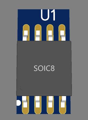
The pcb model is as follows:
The schematic model is as follows:
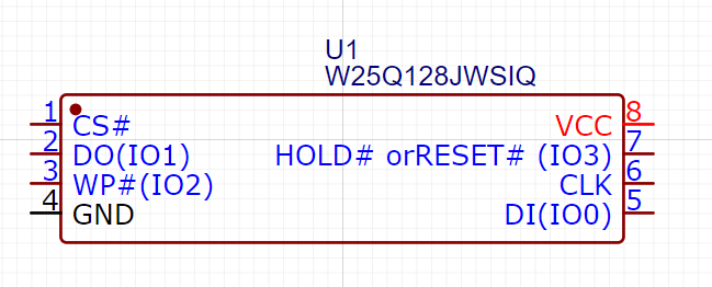
Pin:
Pin 1: CS chip selection signal pin, used for MCU to select peripherals.
Pin 2: DO is sometimes called SO. It is the data output pin of peripheral equipment and the data input pin of MCU, that is, the MISO line connection point of SPI communication.
Pin 3: WP write protection
Pin 4: GND
5 pin: DI, sometimes called SI, is the data input pin of peripheral equipment and the data output pin of MCU, that is, the MOSI line connection point of SPI communication.
Pin 6: CLK is connected to CLK pin of MCU SPI, and the communication clock is provided by this pin.
Pin 7: HOLD
8 pin: VCC
SPI communication accesses peripherals. Generally, MCU is the master device and peripherals are slave devices
2. Capacity
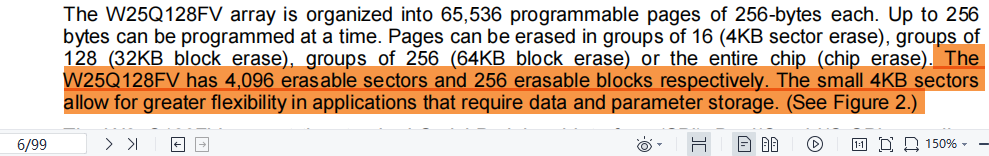
W25Q128 has a capacity of 128M bit, i.e. 128/8=16MB.
W25Q128 consists of 65536 programmable page s. The size of each page is 16MB * 1024 * 1024/65536=256B.
W25Q128 consists of 256 blocks. The capacity of each block is 16MB*1024/256=64KB.
W25Q128 consists of 4096 erasable sectors, so the number of sectors in a block: 4096 / 256 = 16 (number), and the capacity of each sector: 64KB/16=4KB
Sector is the minimum erasure unit of W25Q128, that is, if you want to erase a byte of flash, you must erase all 4KB of the sector in which it is located. If there is other data in this sector, the data needs to be backed up. After erasing the sector, the backed up data can be written back into the sector.
3. Clock
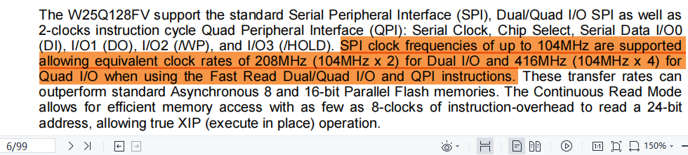
W25Q128 supports standard serial peripheral interface (SPI), dual / fast IO SPI and 2-lock instruction cycle peripheral interface (QPI). When using standard serial peripheral interface (SPI), the clock can support 104MHZ at most; when using dual / fast IO SPI, the equivalent clock rate is 104 *2=208MHZ; when using 2-lock instruction cycle peripheral interface (QPI), the equivalent clock rate is 104 *4=416MHZ
4. On board schematic diagram
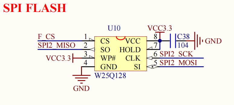
The above figure is the schematic diagram of the board I use. We can see that both write protection (WP) and HOLD are connected to high level. We will know what mode it is when we summarize them later... SO pin is connected to MISO line, SI is connected to MOSI line, CLK is connected to CLK pin of SPI2. The schematic diagram is relatively simple and should not be difficult to understand
To summarize the pin details:
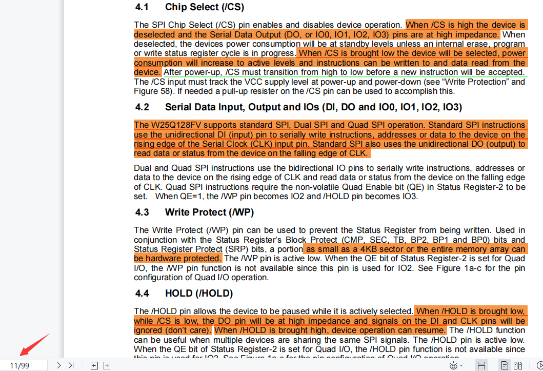
(1) Film selection (CS)
When the CS pin is at high level, the device cannot be selected, and the data output port DO (i.e. SO, MISO) is in high resistance state.
When the CS pin is at low level, the device is selected. At this time, the device can be read and written.
be careful:
After power on, the CS pin must transition from high to low to receive new instructions. Therefore, when initializing W25Q128 in the program, pull the CS pin high and then low.
(2) Serial I / O (DI, DO)
DI pin sends data to the receiving pin of W25Q128 for MCU, and writes data on the rising edge of clock CLK.
DO pin is the data output pin of W25Q128 and is read out at the falling edge of clock CLK.
(3) Write protect (WP)
The write protection low level is active to prevent the status register from being written. The WP pin in the previous schematic diagram is connected to a high level, which invalidates the write protection and can write to the status register at any effective time.
(4)HOLD
Hold can pause the operation, and the low level is valid. When the hold pin is pulled low, if CS is at low level (that is, when the hold pin is pulled low during chip selection peripherals), the signals of DO, DI and CLK pins are ignored. After the hold pin is pulled high, the operation can be resumed.
In the previous schematic diagram, the HOLD pin is connected to a high level, which means that the signals of DI, DO and CLK pins will not be ignored at any effective time.
For details, please refer to the manual of W25Q128:
4. Status register 1 of W25Q128
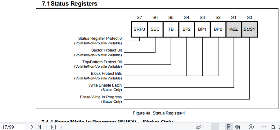
Bit S0 - BUSY:
Busy flag bit, which can only be read. When reading and writing data, erasing sector, erasing block, erasing chip, writing status register and erasing security register are executed, this bit is set to 1. When the operation and instruction are completed, this bit is automatically cleared to 0. The bit flag can be used to judge whether the sector erasure is completed, whether the data writing and reading are completed, etc.
Bit S1 -WEL:
Write enable flag bit, which can only be read. When the write enable instruction is executed, this bit is set to 1. When the write operation is disabled, this bit is cleared.
Bits S2, S3, S4- BP0, BP1, BP2:
Block protection bit to protect the memory block. The default is S4 S3 S2=000. (the details will be summarized together with the following two)
Bit S5-TB:
TB bit, the top and bottom parts are protected, and this bit is 0 by default.
Bit S6-SEC:
SEC bit, sector and block protection bit. This bit is 0 by default.
Next, let's look at the five digits S2, S3, S4, S5 and S6:
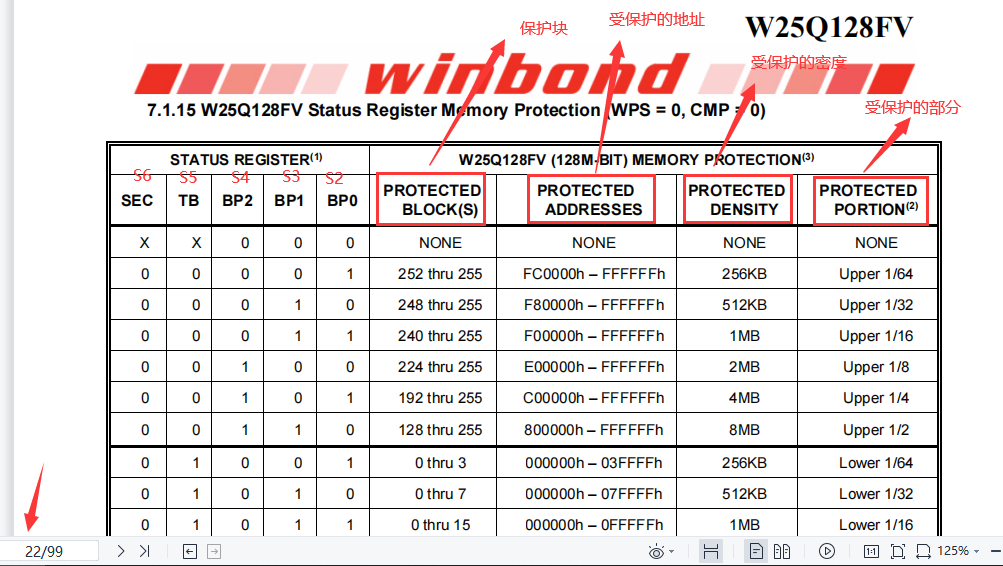
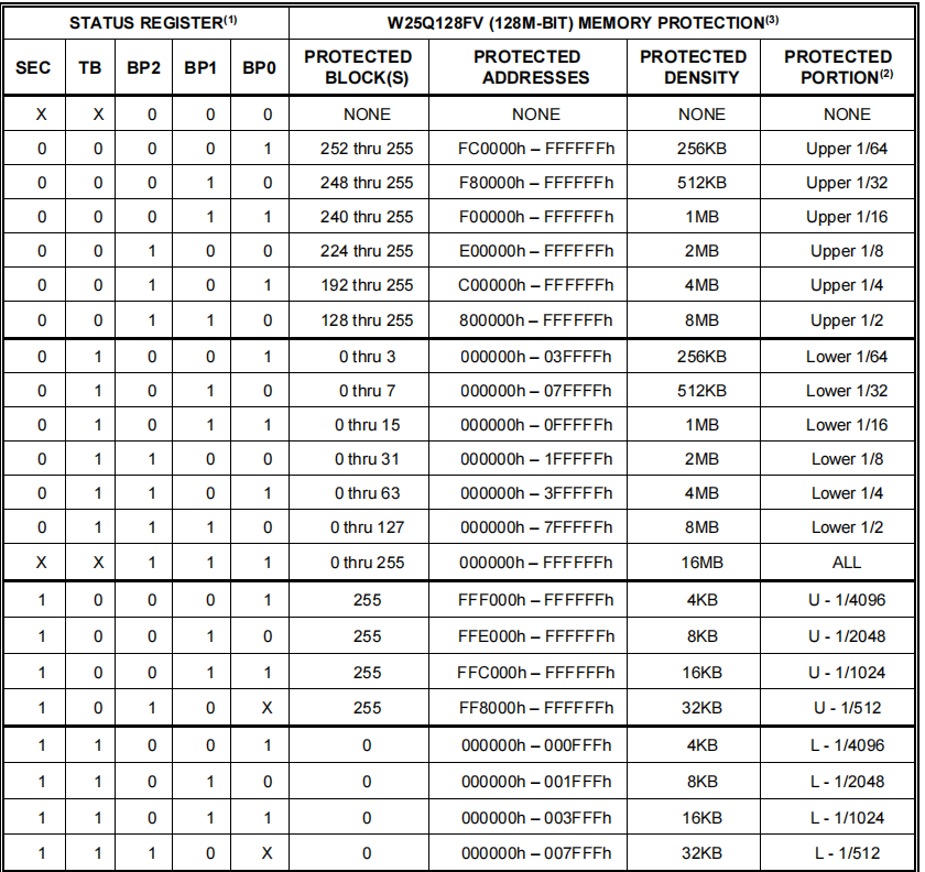
As can be seen from the above table, when BP2, BP1 and BP0 (S4 bit, S3 bit and S2 bit) are all 0 (the first row of the table), all blocks of flash are not protected
In the following table, it is easy to see that different combinations of SEC, TB, PB2, PB1 and PB0 can protect different blocks.
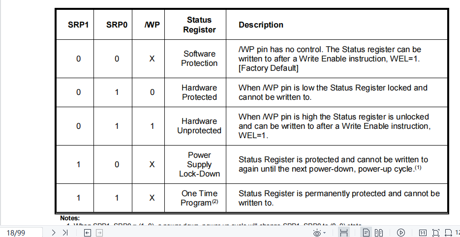
Bit S7-SRP0:
The status register protection 0 is summarized together with the S8 bit of the status register 2.
5. Status register 2 of W25Q128
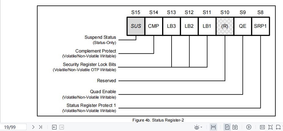
Bit S8-SRP1:
Status register protection 1, used with the S7 bit of the previous register. They can control read and write operations, including software protection, hardware protection, power blocking and one-time programmable protection. The following table:
translate:
| SRP1(S8 bit) | SRP0 (S7 bit) | /WP (write protected) | Register status | describe |
|---|---|---|---|---|
| 0 | 0 | x | software protection | /WP pin is not controlled. After writing the enable instruction, (S1 bit of status register 1) WEL=1, the status register can be written (factory default) |
| 0 | 1 | 0 | Hardware protection | When the / WP pin is low, the status register is locked and cannot be written |
| 0 | 1 | 1 | No hardware protection | When the / WP pin is high, the status register is unlocked, and WEL=1 after writing the enable instruction, |
| 1 | 0 | x | Power lockout | The status register is protected and cannot be written until the next power-off or power-off cycle |
| 1 | 1 | x | One time programming | The status register is permanently protected and cannot be written |
Bit S9-QE:
QPI mode, no summary
Bit S10-R:
Reserved bit
Bits S11, S12, S13-LB1, LB2, LB3:
The unlock bits of the security register are all 0 by default. If both are set to 1, the security register changes to permanent read-only mode.
Bit S14-CMP:
Complementary protection bits are used together with SEC, TB, BP2, BP1 and BP0. If CMP is set to 1, the protected parts set by these bits will no longer be protected, and the unprotected parts will be protected. The default is 0.
Bit S15-SUS:
Pending status flag bit, which is read-only. After the erase and suspend instructions (75h) are executed, this position is 1. After the erase and suspend recovery instructions (7Ah) are executed and the power off and power on cycles are executed, this bit is cleared.
6. Status register 3 of W25Q128
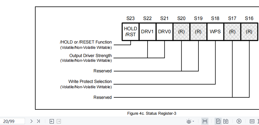
Bits S16, S17, S19 and S20 are reserved bits
Bit S18-WPS:
Write protect select bit.
When WPS=0, the write protection adopts the area protection set by CMP, SEC, TB, BP2, BP1 and BP0.
When WPS=1, a separate block lock is used to protect any sector or block. The default is 1, that is, block lock is used for write protection.
Bits S21, S22-DRV0, DRV1:
Output drive strength setting bit:
| DRV1 | DVR0 | Driving strength |
|---|---|---|
| 0 | 0 | 100% |
| 0 | 1 | 75% |
| 1 | 0 | 50% |
| 1 | 1 | 25% (default) |
Bit S23-HOLD/RST:
HOLD/RST is only valid in QPI mode, and the default value is 0
7. Block address, sector address, page address calculation (important)
It is very important to infer the address range of each block, sector and page when clearing the specified sector. The minimum unit of W25Q128 clearing is sector, and W25Q128 is composed of 256 blocks, each block is 64KB; Each block is composed of 16 sectors, and each sector is 4KB. Because erasing, writing data and reading data all need to pass the address. To accurately find the address of the operation, you need to be able to calculate the address.
Address calculation:
If an address stores 8 bits, that is, an address space stores 1B data, the address increment of a block is 64 * 1024 = 65536
Block 1: 000000 H ~ 00ffffh
Block 2: 010000h~01FFFFh
Block 3: 020000h~02FFFFh
...
Block 11: 0a0000h ~ 0ffffh
...
Block 100: 630000h ~ 63ffh
...
Block 256: ff0000h ~ ffffh
The rule has been seen. The last four digits remain unchanged, all of which are 0000~FFFF. If it is the nth block, the first two digits are hexadecimal numbers (n-1)
Block address rule:
Block n address: (0x)(n-1)0000h~(0x)(n-1)FFFF
Where (0x)(n-1) means: two hexadecimal digits of n-1;
There are 256 blocks in total, just (0x)(n-1) is 00~FF
-----------------------------------------------
-----------------------------------------------
If an address stores 8 bits, that is, an address space stores 1B data, the address increment of a sector is 4 * 1024 = 4096
Address of sector 1 of block 1: 000000 H ~ 000fffh
Address of sector 2 of block 1: 001000h~001FFFh
Address of sector 3 of block 1: 002000h~002FFFh
...
Address of sector 11 of block 1: 00A000h~00AFFFh
...
Address of sector 16 of block 1: 00F000h~00FFFFh
The rule has been seen. The first address range is 000000 H ~ 00ffffh
Then the nth sector: 000000 H + (0x) (n-1) 000h ~ 000000 H + (0x) (n-1) fffh
Another example:
Block 11 address range: 0a0000h ~ 0ffff
Address of sector 1 of block 11: 0A0000h+0000h~0A0000h+0FFFh, i.e. 0A0000h ~0A0FFF;
Address of sector 2 of block 11: 0A0000h+1000h~0A0000h+1FFFh, i.e. 0a10000h ~ 0a1fff;
...
Address of sector 12 of block 11: 0A0000h+B000h~0A0000h+B000h, i.e. 0AB000h ~0ABFFF;
...
Address of sector 16 of block 11: 0A0000h+F000h~0A0000h+F000h, i.e. 0af000h ~ 0ffff;
-----------------------------------------------
-----------------------------------------------
W25Q128 consists of 65536 programmable page s. The size of each page is 16MB10241024/65536=256B. Then the address increment of one page is 256
Page 1 address range: 000000 H ~ 0000ff
Page 2 address range: 000100h ~0001FF
...
Page 11 address range: 000A00h~000AFF
...
Page K address range: (0x)(K-1)00h~(0x)(K-1)FFh
Write the formula together: [(0x) operation: change the following number into hexadecimal number]
Address range of block n: [24 bit address, (0x)(n-1) is 00~FF]
(0x)(n-1)0000h~(0x)(n-1)FFFF
Can be changed to:
(0x){(n-1)×65536} ~ (0x){(n-1)×65536 +65535}
Address range of sector m in block n: [24 bit address, (0x)(n-1) is 00~FF, and (0x)(m-1) is 0 ~F]
(0x)(n-1)0000h+(0x)(m-1)000h~(0x)(n-1)0000h+(0x)(m-1)FFFh
Can be merged into:
{(0x)(n-1) (0x)(m-1) 000h}~{(0x)(n-1) (0x)(m-1) FFFh}
Can be changed to:
(0x){65536×(n-1) +4096×(m-1)} ~ (0x){65536×(n-1) +4096×(m-1)+4095}
As deduced above:
Address of sector 12 of block 11: 0A0000h+B000h~0A0000h+B000h, i.e. 0AB000h ~0ABFFF;
n=11, m=12, using the formula:
(0x)(65536×10 +4096×11) ~ (0x)(65536×10 +4096×11 +4095)
=(0x)700416 ~ (0x)704511
=0AB000~0ABFFF
Address range on page K: [24 bit address, (0x)(K-1) is 0000~FFFF]
(0x)(K-1)00h~(0x)(K-1)FFh
Can be changed to:
(0x){256×(K-1)} ~ (0x){256×(K-1)+255}
If you can't remember, just remember:
Block address: XX0000~XXFFFF
Sector address: XXX000~XXXFFF
Page address: xxx000 ~ xxxxff
XX... Number, starting from 0
2, Peripheral oriented – write functions according to timing
1. MCU end data transfer function
Or follow the code of the previous blog:
u8 SPI2_Send_Data(u8 data)
{
	while(SPI_I2S_GetFlagStatus(SPI2,SPI_I2S_FLAG_TXE)==RESET)
	{
		//The waiting to send cache register is empty
	}
	  SPI_I2S_SendData(SPI2,data);
	while(SPI_I2S_GetFlagStatus(SPI2, SPI_I2S_FLAG_RXNE)==RESET)
	{
		//Wait to receive buffer not empty
	}
	return SPI_I2S_ReceiveData(SPI2);
}
2. Write enable function (instruction: 06h)
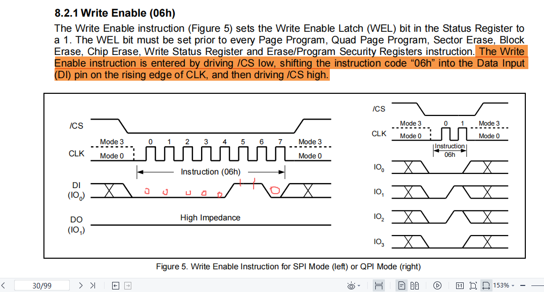
After sending the write enable instruction, the write enable flag bit WEL of the status register 1 is set to 1. By driving the CS low level, input 0x06 to the peripheral through the DI pin at the rising edge of the clock, and then drive the CS pin to high.
Because of the use of film selection, for convenience, define a macro and put it into the header file:
#define CS PBout(12)
code:
//Write enable function instruction: 0x06 (macro definition: Write_Enable)
void W25Q128_Write_Enable(void)						//Write enable function
{
	CS=0;
	SPI2_Send_Data(Write_Enable);
	CS=1;
}
3. Status register write enable function (instruction: 50h)
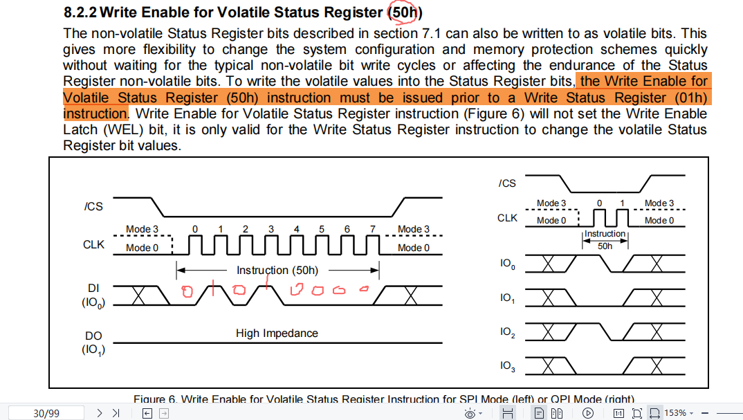
According to the timing, when CS is pulled down, send 0x50 command and pull up CS after completion.
It should be noted that when writing to the status register, you do not need to enable writing (the previous function), that is, you do not operate on the WEL bit of the status register.
code:
//Status register write enable function instruction: 0x50 (macro definition: Status_Register_Write_Enable)
void W25Q128_Status_Register_Write_Enable(void)		//Status register write enable
{
	CS=0;
	SPI2_Send_Data(Status_Register_Write_Enable);
	CS=1;
}
4. Write disable function (instruction: 04h)
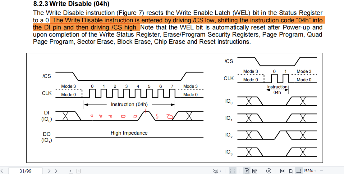
According to the timing, pull CS low, send 0x04 instruction in the next 8 clock cycles, and pull CS high after completion.
After write failure, WEL of status register is set to 0 by hardware.
code:
//Write disable function instruction: 0x04 (macro definition: Write_Disable)
void W25Q128_Write_Disable(void)					//Write disability function
{
	CS=0;
	SPI2_Send_Data(Write_Disable);
	CS=1;
}
5. Read status register function (instruction: 05h, 35h, 15h)
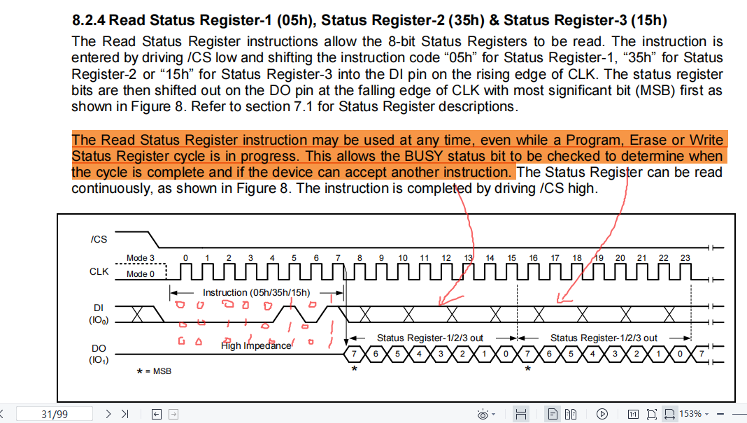
The read status register sends instructions by pulling CS low and transmits instructions within 8 clock cycles. In the next 8 clock cycles, the DO pin outputs the value of the status register (8 bits). The status register can be read continuously, that is, if CS is always at the low level, the value of the status register will be output continuously. When CS is pulled high, the output of the status value will be stopped, and the DO pin will change to the high resistance state.
During SPI communication, the transmission and reception are carried out simultaneously. If the CS is not raised, the status register will be read continuously, and the DI and DO pins will be occupied all the time, so no other operations can be carried out. In order to avoid forgetting to raise the CS and end reading the status register, just raise the CS directly after reading once. If you want to obtain the status register many times, just call this function many times.
The value of the status register needs to be returned. During the period of returning data, the DI pin also has a value, because during SPI communication, MCU needs to send data and receive peripheral data at the same time.
Pass an 8-bit instruction and return an 8-bit status value. Code:
Status register 1:
//Read status register 1 instruction: 0x05 (macro definition: Read_Status_Register1)
u8 W25Q128_Read_Status_Register1(void)			// Read status register 1
{
	u8 temp;
	CS=0;
	SPI2_Send_Data(Read_Status_Register1);
	temp=SPI2_Send_Data(0xff);
	CS=1;
	return temp;
}
Status register 2:
//Read status register 2 instruction: 0x35 (macro definition: Read_Status_Register2)
u8 W25Q128_Read_Status_Register2(void)			// Read status register 2
{
	u8 temp;
	CS=0;
	SPI2_Send_Data(Read_Status_Register2);
	temp=SPI2_Send_Data(0xff);
	CS=1;
	return temp;
}
Status register 3:
//Read status register 3 instruction: 0x15 (macro definition: Read_Status_Register3)
u8 W25Q128_Read_Status_Register3(void)			// Read status register 1
{
	u8 temp;
	CS=0;
	SPI2_Send_Data(Read_Status_Register3);
	temp=SPI2_Send_Data(0xff);
	CS=1;
	return temp;
}
6. Write status register function (instruction: 01h, 31h, 11h)
Not all status registers can be written. Bits capable of writing:
Status register 1: BP0, BP1, TB, SEC, SRP0
Status register 2: SRP1, QE, LB1, LB2, LB3, CMP
Status register 3: WPS, DRV0, DRV1, HOLD
Pay attention to the following paragraph:
Before writing to the status register, write enable the status register write operation; At the same time, keep WEL 0. In other words, before writing to the status register, you must enable the status register write and disable the memory write
Timing:
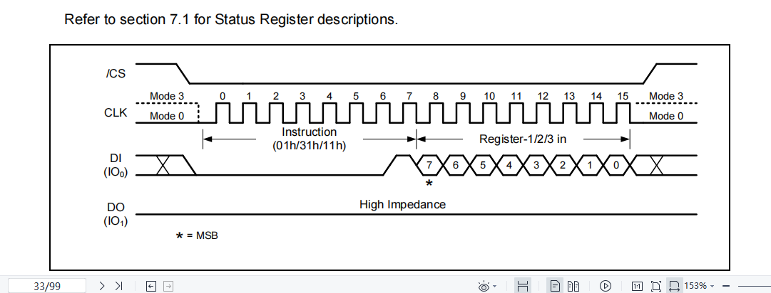
After CS is pulled down, an instruction is passed in, and then the value of the register is passed in. Note that there is no delay period here, so after the instruction is delivered, the value of the status register is directly transmitted.
Write status register 1:
//Write status register 1 instruction: 0x01 (macro definition: Write_Status_Register1)
void W25Q128_Write_Status_Register1(u8 data)		//Write status register 1
{
	W25Q128_Status_Register_Write_Enable();			//Enable register write
	W25Q128_Write_Disable();						//Disable memory write operation
	CS=0;
	SPI2_Send_Data(Write_Status_Register1);
	SPI2_Send_Data(data);
	CS=1;
}
Write status register 2:
//Write status register 2 instruction: 0x31 (macro definition: Write_Status_Register2)
void W25Q128_Write_Status_Register2(u8 data)		//Write status register 2
{
	W25Q128_Status_Register_Write_Enable();			//Enable register write
	W25Q128_Write_Disable();
	CS=0;
	SPI2_Send_Data(Write_Status_Register2);
	SPI2_Send_Data(data);
	CS=1;
}
Write status register 3:
//Write status register 3 instruction: 0x11 (macro definition: Write_Status_Register3)
void W25Q128_Write_Status_Register3(u8 data)		//Write status register 3
{
	W25Q128_Status_Register_Write_Enable();			//Enable register write
	W25Q128_Write_Disable();
	CS=0;
	SPI2_Send_Data(Write_Status_Register3);
	SPI2_Send_Data(data);
	CS=1;
}
7. Read data function (instruction: 03h)
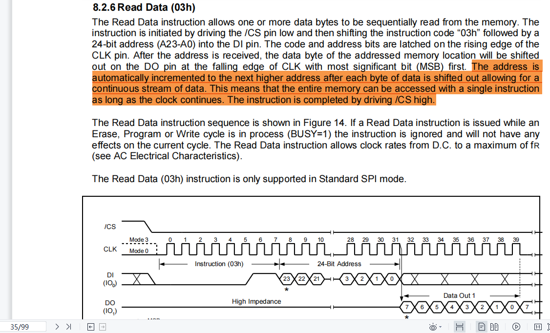
The read data instruction can sequentially read one or more data in memory. After CS is pulled down, send an 8-bit instruction first, and then send a 24 bit address. Then start outputting data. The data can be output continuously. After reading the data in one address space, the address will increase automatically, and then read the data in the next address space. After the address increases to the maximum, it will increase from 0. End reading after CS is pulled up. If CS is not pulled up all the time, you can access the whole memory with a single instruction.
In order to continuously read data, the function needs to transfer not only the 24 bit address, but also the number of bytes to be read. In addition, due to SPI communication, in order to return data, it is necessary to send data to peripherals to return data. The sent data is arbitrary, but the DO pin is always high in the timing, so 0xff is selected as the sent data.
code:
extern u8 buff[65536];
//Read data instruction: 0x03 (macro definition: Read_Data)
void W25Q128_Read_Data(u32 address,u16 num)		//Read data
{
	u16 i;
	CS=0;
	SPI2_Send_Data(Read_Data);
	SPI2_Send_Data((u8)(address>>16));//Send bit 23:16 address
	SPI2_Send_Data((u8)(address>>8));//Send bit 15:8 address
	SPI2_Send_Data((u8)address);//Send bit 7:0 address

	for(i=0;i<num;i++)
	buff[i]=SPI2_Send_Data(0xff);
	CS=1;
}
8. Busy flag wait end function
This function directly accesses the status register 1 without instructions. Code:
void W25Q128_Wait_Busy(void)						//Wait for the BUSY bit of status register 1 to clear
{
	while((W25Q128_Read_Status_Register1()&0x01));
}
9. Page write function (instruction: 02h)
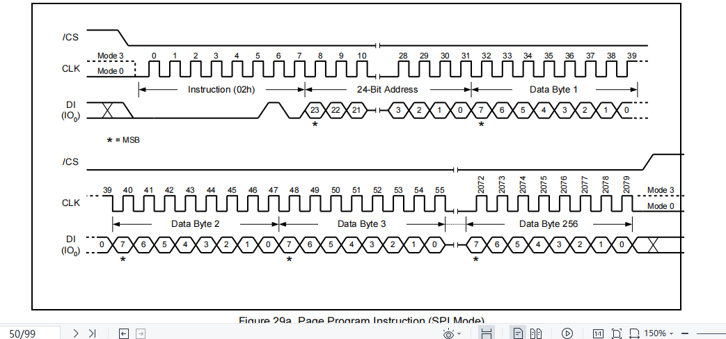
It can be seen that when CS is pulled down, 0x02 instruction is transmitted, and then 24 bit address is transmitted to start writing data to the page.
It should be noted that the size of a page is 256B, so only 256 8-bit data can be imported. If there are more than 256 data, the excess part will be written from the starting address of the page to overwrite the original data. The delivered address can be any address of a page, and then it is stored sequentially from this address. When this page is full, it is stored from the 0 address (xxx000) of this page.
There is also the need to enable write operations before transmitting instructions.
The following sentence:
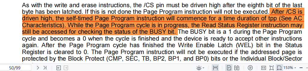
When CS is raised, the page program will start to execute. Therefore, after CS is raised, you need to wait for the busy flag to end.
code:
//Page write data instruction: 0x02 (macro definition: Write_Page)
void W25Q128_Write_page(u32 address,u16 num,u8 buff[])	//Page write data function
{
	u16 i;
	W25Q128_Write_Enable();
	CS=0;
	SPI2_Send_Data(Write_Page);
	SPI2_Send_Data((u8)(address>>16));			//Send bit 23:16 address
	SPI2_Send_Data((u8)(address>>8));			//Send bit 15:8 address
	SPI2_Send_Data((u8)address);				//Send bit 7:0 address

	for(i=0;i<num;i++)
	SPI2_Send_Data(buff[i]);
	CS=1;
	W25Q128_Wait_Busy();
}
10. Sector erase function (instruction: 20h)
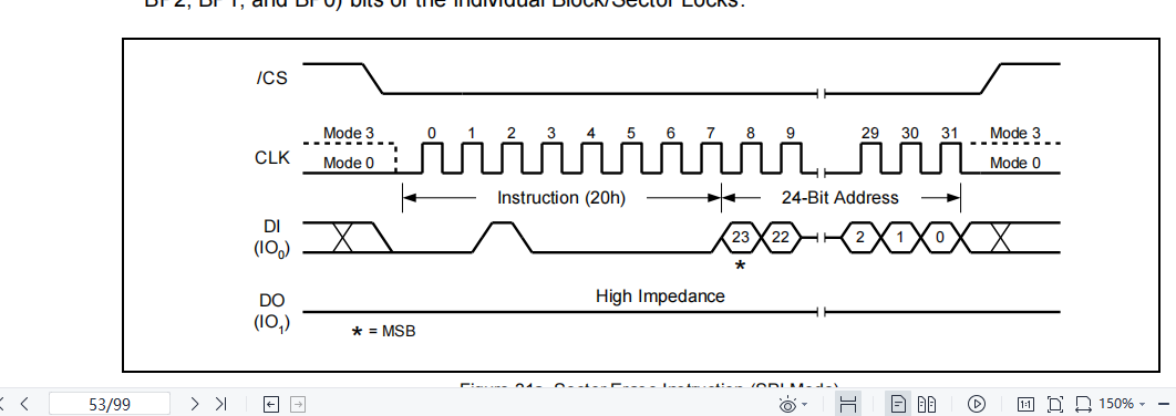
After CS is pulled down, first input an 8-bit instruction, and then pass the address of the erase sector. The calculation of the sector address has been summarized above
The transmitted address can be any address in the sector, which will erase all the data in the sector where the address is located. After the address is transferred, the CS is pulled up to start erasing, otherwise the instruction will not take effect. When erasing, the BUSY bit of the status register is 1, indicating that the erasing instruction is being executed; When the erase is completed, the BUSY bit is cleared to 0.
After sector erasure is completed, the write operation will be automatically disabled. In addition, if block protection is set and the protection area overlaps with the erasure area, the erasure instruction will be invalid.
The write operation must be enabled before the erase instruction is transmitted
Sector erase Code:
//Sector erase function instruction: 0x20 (macro definition: Sector_Erase)
void W25Q128_Sector_Erase(u32 address)				//Sector erase function
{
	W25Q128_Write_Enable();
	CS=0;
	SPI2_Send_Data(Sector_Erase);
	SPI2_Send_Data((u8)(address>>16));				//Send bit 23:16 address
	SPI2_Send_Data((u8)(address>>8));				//Send bit 15:8 address
	SPI2_Send_Data((u8)address);					//Send bit 7:0 address
	CS=1;
	W25Q128_Wait_Busy();							//Wait for erasure to succeed
}
11. Block erase function (instruction: D8h)
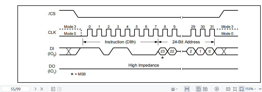
When CS is pulled low, the erase instruction is transmitted in the next 8 clock cycles, and then the 24 bit address is transmitted. Similarly, during the erase process, it is necessary to wait for the BUSY bit to be cleared.
Of course, if block protection is set and the area protected by the block is in the area to be erased, the erase instruction fails.
The write operation must be enabled before the erase instruction is transmitted
code:
//Block erase instruction: 0xD8 (macro definition: Block_Erase)
void W25Q128_Block_Erase(u32 address)				//Block erase
{
	W25Q128_Write_Enable();
	CS=0;
	SPI2_Send_Data(Block_Erase);
	SPI2_Send_Data((u8)(address>>16));				//Send bit 23:16 address
	SPI2_Send_Data((u8)(address>>8));				//Send bit 15:8 address
	SPI2_Send_Data((u8)address);					//Send bit 7:0 address
	CS=1;
	W25Q128_Wait_Busy();							//Wait for erasure to succeed
}
12. Full chip erase function (instruction: C7h or 60h)
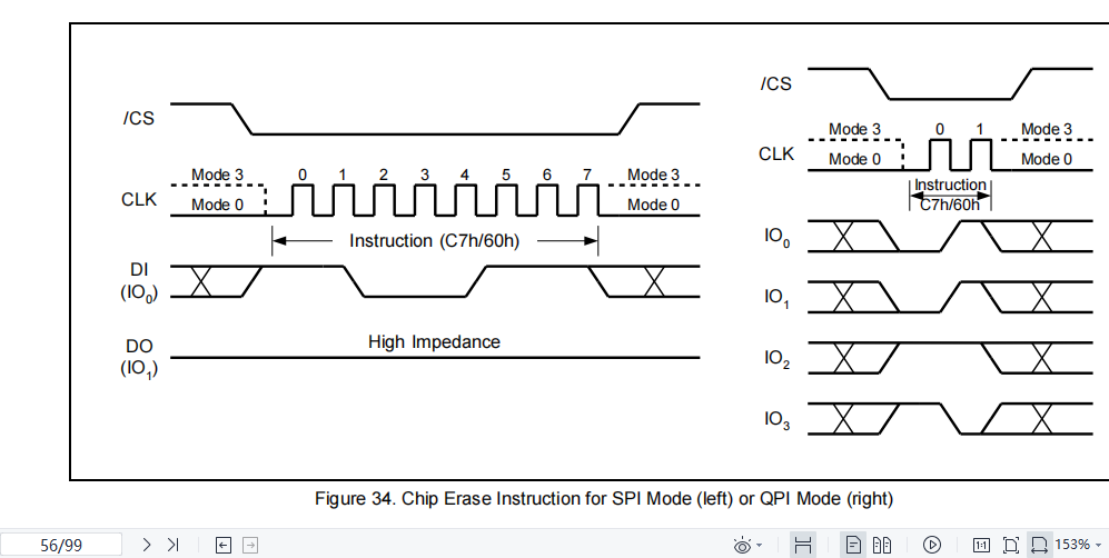
When the CS is pulled low, start to transmit the command. After the command transmission is completed, it is necessary to pull up the CS in time, and then wait for the erasure to be completed.
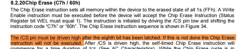
The write operation must be enabled before the erase instruction is transmitted
code:
//Full chip erase instruction: 0xc7 (macro definition: Chip_Erase)
void W25Q128_Chip_Erase(void)						//Full erase
{
	W25Q128_Write_Enable();
	CS=0;
	SPI2_Send_Data(Chip_Erase);
	CS=1;
	W25Q128_Wait_Busy();							//Wait for erasure to succeed
}
13. Erase pause function (instruction: 75h)
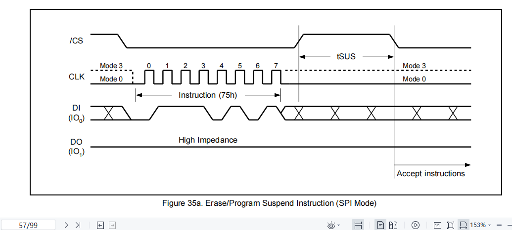
After CS is pulled low, the command is transmitted. After the command transmission is completed, it enters the erase pause state.
After entering the pause state, you can receive new instructions, such as reading data from other areas, after tSUS (the maximum is 20us by looking up the table).
Erase pause is only valid for sector erase, block erase and page erase, but not for full chip erase
Writing status register 1 and various erase instructions is not allowed during erase pause.
After the erase pause, the SUS of status register 2 is set to 1, indicating that it has been suspended, and the BUSY of status register 1 is cleared to receive other instructions for other operations.
code:
//Pause erase function instruction: 0x75 (macro definition: Suspend_Erase)
void W25Q128_Suspend_Erase(void)					//Erase pause function
{
	CS=0;
	SPI2_Send_Data(Suspend_Erase);
	CS=1;
}
14. Erase recovery function (instruction: 7Ah)
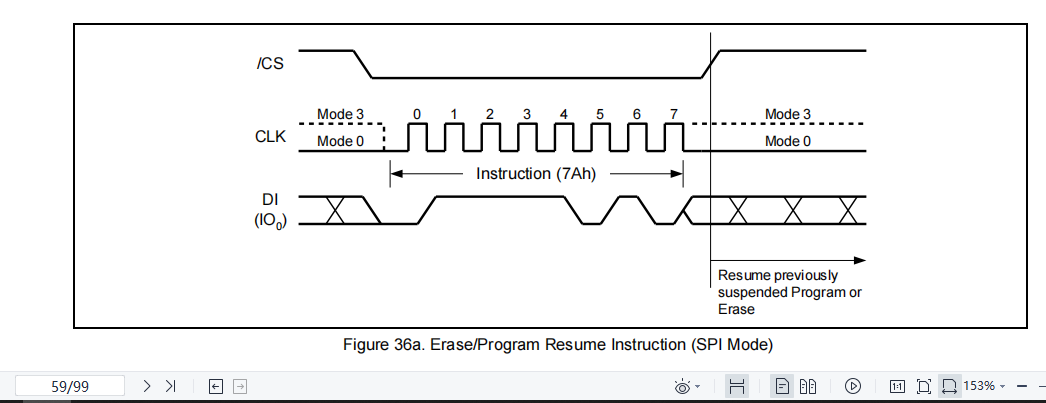
After CS is pulled low, transmit the restore erase command, and then immediately pull CS high to restore the original erase state.
code:
//Restore erase function instruction: 0x7a (macro definition: Resume_Erase)
void W25Q128_Resume_Erase(void)					//Restore erase
{
	CS=0;
	SPI2_Send_Data(Resume_Erase);
	CS=1;
}
15. Power down function (instruction: B9h)
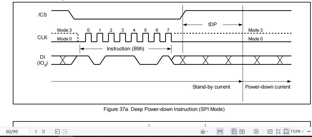
When CS is pulled low, send power down command, and pull up CS immediately after command transmission
The power down mode is to reduce the power consumption of W25Q128. In the power down mode, the peripheral can only recognize and release the power down and device ID instructions, and other instructions will be ignored.
code:
//Power down function instruction: B9h (macro definition: Power_Down)
void W25Q128_Power_Down(void)						//Power down function
{
	CS=0;
	SPI2_Send_Data(Power_Down);
	CS=1;
}
16. Power down recovery function (instruction: ABh)
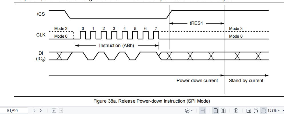
When CS is pulled low, send power down command, and pull up CS immediately after command transmission.
code:
//Release power down function instruction: ABh (macro definition: retain_power_down)
void W25Q128_Release_Power_Down(void)				//Release power down function
{
	CS=0;
	SPI2_Send_Data(Rekease_Power_Down);
	CS=1;
}
17. Read manufacturer ID and device ID function (instruction: 90h)
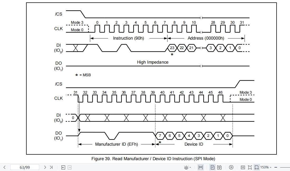
After CS is pulled low, first send the command, then send the 24 bit 000000 h, and then output the manufacturer ID of the upper eight bits and the device ID of the lower 16 bits at the DO pin.
It should be noted that in the block of cycles 31 ~ 46 in the above figure, the MCU is reading peripheral data, so it is necessary for the MCU to send 0xff (usually) while receiving. As for the functions summarized above, they are instruction write operations. In fact, the peripheral has returned bytes, and all the previous timing DO S are set to high level, indicating that when the MCU writes, the peripheral returns 0xff at the same time, which is just ignored by the MCU.
code:
//Read manufacturer ID and device ID instruction: 0x90 (macro definition: Read_ID)
u16 W25Q128_Read_ID(void)							//Read manufacturer ID (upper eight digits) and device ID (lower eight digits)
{
	u16 temp;
	CS=0;
	SPI2_Send_Data(Read_ID);
	SPI2_Send_Data(0x00);
	SPI2_Send_Data(0x00);
	SPI2_Send_Data(0x00);
	temp=SPI2_Send_Data(0xFF)<<8;
	temp+=SPI2_Send_Data(0xFF);
	CS=1;
}
18. Sequential write function
The previous function for W25Q128 write operation written according to timing only supports page write. If all write operations use this page write function, it is particularly troublesome. It is not only necessary to judge which page the address is on, but also calculate the first address of the next page after writing this page, and then call the page write function again.
So write a function written in sequence. The address is automatically calculated in the function. The function parameters only need to pass the first address, quantity and array of stored data.
W25Q128 has 65536 pages, the capacity of each page is 256B, and the address of each page is xxx000 ~ xxxxff
Thought:
After the function passes the first address and the number of writes, the function starts to calculate: how many address spaces are left in this page (calculated from the first address passed), how many complete pages are needed, and how many address spaces are needed in the last page (the last page is generally not enough)
After the calculation, start to store. First save the first page. At this time, remove the saved number and move the array to the left. After that is the writing of several complete pages... The writing of the last page
code:
void W25Q128_Sequential_Write(u32 address,u32 num,u8 buff[])//Sequential write
{
	//Occupied page calculation
	u16 a,b,i,j;
	u32 address_num;
	address_num=(address|0x0000ff)-address;//How much address space is left on the first page
	a=(num-address_num)/256;//In addition to this page, how many complete pages do you need to use next
	b=(num-address_num)%256;//How many copies of the last page need to be saved

	if(address_num>=num)//Just save the data to this page
		W25Q128_Write_page(address,num,buff);//Write all data to

	if(address_num<num)
	{
		W25Q128_Write_page(address,num,buff);//Write the data of the first page to address_num data
		for(i=address_num;i<num;i++)
			buff[i-address_num]=buff[i];//Move the data not written to the left to the beginning of the array

		if(a)//Next, there is a full page to write
		{
			for(j=0;j<a;j++)
			{
				W25Q128_Write_page((address&0xffff00)+256*(j+1),256,buff);
				for(i=256;i<num;i++)
					buff[i-256]=buff[i];//Move the data not written to the left to the beginning of the array
			}
		}
		if(b)//The last page has some data to input
		{
			W25Q128_Write_page((address&0xffff00)+256*(a+1),b,buff);
		}

	}
}
The above code can realize the function, but it is not recommended, because the assignment of a large number of array data will take a lot of time and is not the optimal solution.
Therefore, the code is modified. The array is not moved to the left. A parameter is directly passed to indicate which bit of the array the data to be written next time starts.
The following page write function is modified to facilitate Calling:
//Page write data function (revision, serving W25Q128_Sequential_Write(), not used under normal circumstances)
//Normally, you can also use the parameter begin = 0 to write from the first bit of the array
//Instead of reading data from buff[0], the page is written from buff[begin]
void W25Q128_Write_page_again(u32 address,u16 num,u16 begin,u8 buff[])
{
	u16 i;
	W25Q128_Write_Enable();
	CS=0;
	SPI2_Send_Data(Write_Page);
	SPI2_Send_Data((u8)(address>>16));			//Send bit 23:16 address
	SPI2_Send_Data((u8)(address>>8));			//Send bit 15:8 address
	SPI2_Send_Data((u8)address);				//Send bit 7:0 address

	for(i=begin;i<begin+num;i++)
	SPI2_Send_Data(buff[i]);
	CS=1;
	W25Q128_Wait_Busy();
}
Sequential write function: [recommended]
void W25Q128_Sequential_Write(u32 address,u32 num,u8 buff[])//Sequential write
{
	//Occupied page calculation
	u16 a,b,i,j;
	u32 address_num;
	address_num=(address|0x0000ff)-address+1;//How much address space is left on the first page
	a=(num-address_num)/256;//In addition to this page, how many complete pages do you need to use next
	b=(num-address_num)%256;//How many copies of the last page need to be saved

	if(address_num>=num)//Just save the data to this page
		W25Q128_Write_page(address,num,buff);//Write all data to

	if(address_num<num)
	{
		W25Q128_Write_page(address,address_num,buff);//Write the data of the first page to address_num data

		if(a)//Next, there is a full page to write
		{
			for(j=0;j<a;j++)
			{
				W25Q128_Write_page_again((address&0xffff00)+256*(j+1),256,address_num+j*256,buff);
			}
		}
		if(b)//The last page has some data to input
		{
			W25Q128_Write_page_again((address&0xffff00)+256*(a+1),b,address_num+a*256,buff);
		}
	}
}
19. Sequential read function
In fact, the previous read function is read in sequence, but in order to align with the sequential write function, wrap the previous function:
void W25Q128_Sequential_Read(u32 address,u16 num)//Sequential reading
{
	W25Q128_Read_Data(address,num);
}
19. Sequential erase function
The previously written erase function can not be well referenced in practical application, because when the whole block and the whole sector are erased, we don't want to erase some data, so we should back up the data and write the data we don't want to erase after erasing. So write a sequential erase function.
Core idea:
(1) If the erased area is only in a sector, first calculate the number of address spaces before and after the erased segment, and then back up the data of these address spaces. After erasing this sector, write the backed up data to the original location.
(2) If the erased area occupies several sectors, first calculate the address space occupied by the first half of the first sector and the address space occupied by the second half of the last sector, and back up these data. Count the number of complete sectors occupied by the erased section, and then erase the sectors after counting the number of sectors
After clearing, write the data just backed up to the original location.
(3) If there are a lot of deleted data, block erasure can be considered, but data backup will cause great trouble. For example, the first part of the erasure segment only occupies the last few addresses of the block, so it is obviously unrealistic to back up 6W + data.
(4) Block erasure and sector erasure can be mixed to solve the problem of data backup. This method is the best (block erasure is suitable for erasing too much data, and sector erasure is suitable for erasing less data). In fact, sector erasure is good for all, and the time is about the same.
code:
u8 arr1[0xfff];//When a single sector is erased, the data in the first half of the sector is stored
void W25Q128_Sequential_Erase(u32 address,u32 num)		//Sequential erase
{
	u16 a,b,i;
	u32 address_num;
	address_num=(address|0x000fff)-address+1;//Back area capacity of this sector
	a=(num-address_num)/4096;//In addition to this sector, several complete sectors need to be cleared
	b=(num-address_num)%4096;//How many address spaces does the last sector need to clear

	//First sector operation
	if(address_num>=num)//Cross sector erasure is not required
	{
		W25Q128_Read_Data(address&0xfff000,address-(address&0xfff000));//Read data that does not need to be erased and store it (the data of the first half of the backup Sector)
		for(i=0;i<4096-address_num;i++)
			arr1[i]=read_buff[i];//Back up the data in front of the sector that is not deleted to the arr1 array

		W25Q128_Read_Data(address+num,(address|0x000fff)-(address+num)-1);//Read and store data that does not need to be erased (the data of the second half of the backup Sector)

		W25Q128_Sector_Erase(address);//Erase sector

		W25Q128_Sequential_Write(address&0xfff000,address-(address&0xfff000),arr1);//Re write the backed up data after erasure (first half)
		W25Q128_Sequential_Write(address+num,(address|0x000fff)-(address+num)-1,read_buff);//Re write the backed up data after erasure (the second half)

	}
	else//Cross sector erasure required
	{
		W25Q128_Read_Data(address&0xfff000,4096-address_num);//Read data that does not need to be erased and store it (the data of the first half of the backup Sector)
		W25Q128_Sector_Erase(address);//Erase sector
		W25Q128_Sequential_Write(address&0xfff000,4096-address_num,read_buff);//Re write the backed up data after erasure
		if(a)
		{
			for(i=0;i<a;i++)
				W25Q128_Sector_Erase((address&0xfff000)+4096*(i+1));
		}
		if(b)
		{
			W25Q128_Read_Data((address&0xfff000)+4096*(a+1)+b,4096-b);//Read and store data that does not need to be erased (the data of the second half of the backup Sector)
			W25Q128_Sector_Erase((address&0xfff000)+4096*(a+1));//Erase sector
			W25Q128_Sequential_Write((address&0xfff000)+4096*(a+1)+b,4096-b,read_buff);//Re write the backed up data after erasure
		}
	}
}
20. Group photo of all functions
(after that, the code of the test part will not be put, too long!)
w25q128.h file
#ifndef _w25Q128_
#define _w25Q128_
#include "stm32f10x.h"
#include "spi.h"
#include "sys.h"
#define CS 	PBout(12)

/*-----Instruction list------*/
#define Write_Enable 					 0x06 / / write enable instruction
#define 	 Status_Register_Write_Enable 	 0x50 	// Status register write enable
#define Write_Disable 					 0x04 	// Write disability
#define Read_Status_Register1 			 0x05 	// Read status register 1
#define Read_Status_Register2 			 0x35 	// Read status register 2
#define Read_Status_Register3 			 0x15 	// Read status register 3
#define Write_Status_Register1 			 0x01 	// Write status register 1
#define Write_Status_Register2 			 0x31 	// Write status register 2
#define Write_Status_Register3 			 0x11 	// Write status register 3
#define Read_Data 						 0x03 	// Read data instruction
#define Write_Page 						 0x02 	// Page write instruction
#define Sector_Erase 					 0x20 	// Sector erase instruction
#define Block_Erase 						 0xD8 	// Block erase instruction
#define Chip_Erase 						 0xC7 	// Full erase
#define 	 Suspend_Erase 					 0x75 	// Erase pause
#define Resume_Erase 					 0x7A 	// Restore erase
#define Power_Down 						 0xB9 	// Power failure
#define Rekease_Power_Down 				 0xAB 	// Release power down
#define Read_ID 							 0x90 	// Read ID

//void W25Q128_Init(void);
void W25Q128_Write_Enable(void);						//Write enable function
void W25Q128_Status_Register_Write_Enable(void);		//Status register write enable
void W25Q128_Write_Disable(void);						//Write disability function
u8 W25Q128_Read_Status_Register1(void);					// Read status register 1
u8 W25Q128_Read_Status_Register2(void);					// Read status register 2
u8 W25Q128_Read_Status_Register3(void);					// Read status register 3
void W25Q128_Write_Status_Register1(u8 data);			//Write status register 1
void W25Q128_Write_Status_Register2(u8 data);			//Write status register 2
void W25Q128_Write_Status_Register3(u8 data);			//Write status register 3
void W25Q128_Read_Data(u32 address,u16 num);			//Read data
void W25Q128_Write_page(u32 address,u16 num,u8 *);		//Page write data function
void W25Q128_Wait_Busy(void);							//Wait for the BUSY bit of status register 1 to clear
void W25Q128_Sector_Erase(u32 address);					//Sector erase function
void W25Q128_Block_Erase(u32 address);					//Block erase
void W25Q128_Chip_Erase(void);							//Full erase
void W25Q128_Suspend_Erase(void);						//Erase pause function
void W25Q128_Resume_Erase(void);						//Restore erase
void W25Q128_Power_Down(void);							//Power down function
void W25Q128_Release_Power_Down(void);					//Release power down function
u16 W25Q128_Read_ID(void);								//Read manufacturer ID (upper eight digits) and device ID (lower eight digits)

void W25Q128_Write_page_again(u32 address,u16 num,u16 begin,u8 *);
//Page write data function (revision, serving W25Q128_Sequential_Write(), not used under normal circumstances)


void W25Q128_Sequential_Write(u32 address,u32 num,u8 *);//Sequential write
void W25Q128_Sequential_Read(u32 address,u16 num);		//Sequential reading
void W25Q128_Sequential_Erase(u32 address,u32 num);		//Sequential erase
#endif
w25q128.c code:
#include "stm32f10x.h"
#include "w25q128.h"
extern u8 read_buff[0XFFF];//Note that the size of this array should not be changed. It also serves the data backup of sector erasure

//Write enable function instruction: 0x06 (macro definition: Write_Enable)
void W25Q128_Write_Enable(void)						//Write enable function
{
	CS=0;
	SPI2_Send_Data(Write_Enable);
	CS=1;
}

//Status register write enable function instruction: 0x50 (macro definition: Status_Register_Write_Enable)
void W25Q128_Status_Register_Write_Enable(void)		//Status register write enable
{
	CS=0;
	SPI2_Send_Data(Status_Register_Write_Enable);
	CS=1;
}


//Write disable function instruction: 0x04 (macro definition: Write_Disable)
void W25Q128_Write_Disable(void)					//Write disability function
{
	CS=0;
	SPI2_Send_Data(Write_Disable);
	CS=1;
}

//Read status register 1 instruction: 0x05 (macro definition: Read_Status_Register1)
u8 W25Q128_Read_Status_Register1(void)			// Read status register 1
{
	u8 temp;
	CS=0;
	SPI2_Send_Data(Read_Status_Register1);
	temp=SPI2_Send_Data(0xff);
	CS=1;
	return temp;
}

//Read status register 2 instruction: 0x35 (macro definition: Read_Status_Register2)
u8 W25Q128_Read_Status_Register2(void)			// Read status register 2
{
	u8 temp;
	CS=0;
	SPI2_Send_Data(Read_Status_Register2);
	temp=SPI2_Send_Data(0xff);
	CS=1;
	return temp;
}

//Read status register 3 instruction: 0x15 (macro definition: Read_Status_Register3)
u8 W25Q128_Read_Status_Register3(void)			// Read status register 1
{
	u8 temp;
	CS=0;
	SPI2_Send_Data(Read_Status_Register3);
	temp=SPI2_Send_Data(0xff);
	CS=1;
	return temp;
}

//Write status register 1 instruction: 0x01 (macro definition: Write_Status_Register1)
void W25Q128_Write_Status_Register1(u8 data)		//Write status register 1
{
	W25Q128_Status_Register_Write_Enable();			//Enable register write
	W25Q128_Write_Disable();						//Disable memory write operation
	CS=0;
	SPI2_Send_Data(Write_Status_Register1);
	SPI2_Send_Data(data);
	CS=1;
}

//Write status register 2 instruction: 0x31 (macro definition: Write_Status_Register2)
void W25Q128_Write_Status_Register2(u8 data)		//Write status register 2
{
	W25Q128_Status_Register_Write_Enable();			//Enable register write
	W25Q128_Write_Disable();
	CS=0;
	SPI2_Send_Data(Write_Status_Register2);
	SPI2_Send_Data(data);
	CS=1;
}

//Write status register 3 instruction: 0x11 (macro definition: Write_Status_Register3)
void W25Q128_Write_Status_Register3(u8 data)		//Write status register 3
{
	W25Q128_Status_Register_Write_Enable();			//Enable register write
	W25Q128_Write_Disable();
	CS=0;
	SPI2_Send_Data(Write_Status_Register3);
	SPI2_Send_Data(data);
	CS=1;
}

//Read data instruction: 0x03 (macro definition: Read_Data)
void W25Q128_Read_Data(u32 address,u16 num)		  //Read data
{
	u16 i;
	CS=0;
	SPI2_Send_Data(Read_Data);
	SPI2_Send_Data((u8)(address>>16));			//Send bit 23:16 address
	SPI2_Send_Data((u8)(address>>8));			//Send bit 15:8 address
	SPI2_Send_Data((u8)address);				//Send bit 7:0 address

	for(i=0;i<num;i++)
	read_buff[i]=SPI2_Send_Data(0xff);
	CS=1;
}

//Page write data instruction: 0x02 (macro definition: Write_Page)
void W25Q128_Write_page(u32 address,u16 num,u8 buff[])	//Page write data function
{
	u16 i;
	W25Q128_Write_Enable();
	CS=0;
	SPI2_Send_Data(Write_Page);
	SPI2_Send_Data((u8)(address>>16));			//Send bit 23:16 address
	SPI2_Send_Data((u8)(address>>8));			//Send bit 15:8 address
	SPI2_Send_Data((u8)address);				//Send bit 7:0 address

	for(i=0;i<num;i++)
	SPI2_Send_Data(buff[i]);
	CS=1;
	W25Q128_Wait_Busy();

}


void W25Q128_Wait_Busy(void)	//Wait for the BUSY bit of status register 1 to clear
{

	while((W25Q128_Read_Status_Register1()&0x01));

}

//Sector erase function instruction: 0x20 (macro definition: Sector_Erase)
void W25Q128_Sector_Erase(u32 address)				//Sector erase function
{
	W25Q128_Write_Enable();
	CS=0;
	SPI2_Send_Data(Sector_Erase);
	SPI2_Send_Data((u8)(address>>16));				//Send bit 23:16 address
	SPI2_Send_Data((u8)(address>>8));				//Send bit 15:8 address
	SPI2_Send_Data((u8)address);					//Send bit 7:0 address
	CS=1;
	W25Q128_Wait_Busy();							//Wait for erasure to succeed

}

//Block erase instruction: 0xD8 (macro definition: Block_Erase)
void W25Q128_Block_Erase(u32 address)				//Block erase
{
	W25Q128_Write_Enable();
	CS=0;
	SPI2_Send_Data(Block_Erase);
	SPI2_Send_Data((u8)(address>>16));				//Send bit 23:16 address
	SPI2_Send_Data((u8)(address>>8));				//Send bit 15:8 address
	SPI2_Send_Data((u8)address);					//Send bit 7:0 address
	CS=1;
	W25Q128_Wait_Busy();							//Wait for erasure to succeed
}

//Full chip erase instruction: 0xc7 (macro definition: Chip_Erase)
void W25Q128_Chip_Erase(void)						//Full erase
{
	W25Q128_Write_Enable();
	W25Q128_Wait_Busy();
	CS=0;
	SPI2_Send_Data(Chip_Erase);
	CS=1;
	W25Q128_Wait_Busy();					//Wait for erasure to succeed
}


//Pause erase function instruction: 0x75 (macro definition: Suspend_Erase)
void W25Q128_Suspend_Erase(void)			//Erase pause function
{
	CS=0;
	SPI2_Send_Data(Suspend_Erase);
	CS=1;
}


//Restore erase function instruction: 0x7a (macro definition: Resume_Erase)
void W25Q128_Resume_Erase(void)				//Restore erase
{
	CS=0;
	SPI2_Send_Data(Resume_Erase);
	CS=1;
}


//Power down function instruction: B9h (macro definition: Power_Down)
void W25Q128_Power_Down(void)						//Power down function
{
	CS=0;
	SPI2_Send_Data(Power_Down);
	CS=1;
}


//Release power down function instruction: ABh (macro definition: retain_power_down)
void W25Q128_Release_Power_Down(void)				//Release power down function
{
	CS=0;
	SPI2_Send_Data(Rekease_Power_Down);
	CS=1;
}

//Read manufacturer ID and device ID instruction: 0x90 (macro definition: Read_ID)
u16 W25Q128_Read_ID(void)//Read manufacturer ID (upper eight digits) and device ID (lower eight digits)
{
	u16 temp;
	CS=0;
	SPI2_Send_Data(Read_ID);
	SPI2_Send_Data(0x00);
	SPI2_Send_Data(0x00);
	SPI2_Send_Data(0x00);
	temp=SPI2_Send_Data(0xFF)<<8;
	temp+=SPI2_Send_Data(0xFF);
	CS=1;
	return temp;

}

//Page write data function (revision, serving W25Q128_Sequential_Write(), not used under normal circumstances)
//Normally, you can also use the parameter begin = 0 to write from the first bit of the array
//Instead of reading data from buff[0], the page is written from buff[begin]
void W25Q128_Write_page_again(u32 address,u16 num,u16 begin,u8 buff[])
{
	u16 i;
	W25Q128_Write_Enable();
	CS=0;
	SPI2_Send_Data(Write_Page);
	SPI2_Send_Data((u8)(address>>16));			//Send bit 23:16 address
	SPI2_Send_Data((u8)(address>>8));			//Send bit 15:8 address
	SPI2_Send_Data((u8)address);				//Send bit 7:0 address

	for(i=begin;i<begin+num;i++)
	SPI2_Send_Data(buff[i]);
	CS=1;
	W25Q128_Wait_Busy();
}

//Sequential write
void W25Q128_Sequential_Write(u32 address,u32 num,u8 buff[])//Sequential write
{
	//Occupied page calculation
	u16 a,b,i,j;
	u32 address_num;
	address_num=(address|0x0000ff)-address+1;//How much address space is left on the first page
	a=(num-address_num)/256;//In addition to this page, how many complete pages do you need to use next
	b=(num-address_num)%256;//How many copies of the last page need to be saved

	if(address_num>=num)//Just save the data to this page
		W25Q128_Write_page(address,num,buff);//Write all data to

	if(address_num<num)
	{
		W25Q128_Write_page(address,address_num,buff);//Write the data of the first page to address_num data

		if(a)//Next, there is a full page to write
		{
			for(j=0;j<a;j++)
			{
				W25Q128_Write_page_again((address&0xffff00)+256*(j+1),256,address_num+j*256,buff);
			}
		}
		if(b)//The last page has some data to input
		{
			W25Q128_Write_page_again((address&0xffff00)+256*(a+1),b,address_num+a*256,buff);
		}
	}
}

//Sequential reading
void W25Q128_Sequential_Read(u32 address,u16 num)//Sequential reading
{
	W25Q128_Read_Data(address,num);
}

//Sequential erase
u8 arr1[0xfff];//When a single sector is erased, the data in the first half of the sector is stored
void W25Q128_Sequential_Erase(u32 address,u32 num)		//Sequential erase
{

	u16 a,b,i;
	u32 address_num;
	address_num=(address|0x000fff)-address+1;//Back area capacity of this sector
	a=(num-address_num)/4096;//In addition to this sector, several complete sectors need to be cleared
	b=(num-address_num)%4096;//How many address spaces does the last sector need to clear

	//First sector operation
	if(address_num>=num)//Cross sector erasure is not required
	{
		W25Q128_Read_Data(address&0xfff000,address-(address&0xfff000));//Read data that does not need to be erased and store it (the data of the first half of the backup Sector)
		for(i=0;i<4096-address_num;i++)
			arr1[i]=read_buff[i];//Back up the data in front of the sector that is not deleted to the arr1 array

		W25Q128_Read_Data(address+num,(address|0x000fff)-(address+num)-1);//Read and store data that does not need to be erased (the data of the second half of the backup Sector)

		W25Q128_Sector_Erase(address);//Erase sector

		W25Q128_Sequential_Write(address&0xfff000,address-(address&0xfff000),arr1);//Re write the backed up data after erasure (first half)
		W25Q128_Sequential_Write(address+num,(address|0x000fff)-(address+num)-1,read_buff);//Re write the backed up data after erasure (the second half)

	}
	else//Cross sector erasure required
	{

		W25Q128_Read_Data(address&0xfff000,4096-address_num);//Read data that does not need to be erased and store it (the data of the first half of the backup Sector)
		W25Q128_Sector_Erase(address);//Erase sector
		W25Q128_Sequential_Write(address&0xfff000,4096-address_num,read_buff);//Re write the backed up data after erasure
		if(a)
		{
			for(i=0;i<a;i++)
				W25Q128_Sector_Erase((address&0xfff000)+4096*(i+1));
		}
		if(b)
		{
			W25Q128_Read_Data((address&0xfff000)+4096*(a+1)+b,4096-b);//Read and store data that does not need to be erased (the data of the second half of the backup Sector)
			W25Q128_Sector_Erase((address&0xfff000)+4096*(a+1));//Erase sector
			W25Q128_Sequential_Write((address&0xfff000)+4096*(a+1)+b,4096-b,read_buff);//Re write the backed up data after erasure
		}
	}
}
3, Function test
Put the SPI first H and SPI c
Let's put the SPI first H and SPI C code:
spi.h code
#ifndef _SPI_
#define _SPI_
#include "stm32f10x.h"
void MySPI_Init(void);
u8 SPI2_Send_Data(u8 data);//Data transfer function
#endif
spi.c code
#include "spi.h"
#include "stm32f10x.h"
#include "w25q128.h"

void MySPI_Init(void)
{
/*
	PB12-----SPI2_NSS----->W25Q128 CS pin of (software mode, NSS as normal IO)
	PB13-----SPI2_SCK----->W25Q128 CLK pin of
	PB14-----SPI2_MISO---->W25Q128 S0(D0) pin of
	PB15-----SPI2_MOSI---->W25Q128 SI(DI) pin of
*/
	GPIO_InitTypeDef  GPIO_InitStructure;
	SPI_InitTypeDef  SPI_InitStructure;

	RCC_APB2PeriphClockCmd(RCC_APB2Periph_GPIOB, ENABLE);
	RCC_APB1PeriphClockCmd(	RCC_APB1Periph_SPI2,  ENABLE );


	GPIO_InitStructure.GPIO_Mode=GPIO_Mode_AF_PP;
	GPIO_InitStructure.GPIO_Pin=GPIO_Pin_13|GPIO_Pin_14|GPIO_Pin_15; //PB13, 14 and 15 are multiplexed Push-Pull Outputs
	GPIO_InitStructure.GPIO_Speed=GPIO_Speed_50MHz;
	GPIO_Init(GPIOB,&GPIO_InitStructure);
	GPIO_SetBits(GPIOB,GPIO_Pin_13|GPIO_Pin_14|GPIO_Pin_15);  //The initial state is high

	GPIO_InitStructure.GPIO_Mode=GPIO_Mode_Out_PP;
	GPIO_InitStructure.GPIO_Pin=GPIO_Pin_12; //Chip selection signal, universal push-pull output
	GPIO_InitStructure.GPIO_Speed=GPIO_Speed_50MHz;
	GPIO_Init(GPIOB,&GPIO_InitStructure);
	CS=1;//The initial state is not selected

	SPI_InitStructure.SPI_BaudRatePrescaler=SPI_BaudRatePrescaler_2;
	SPI_InitStructure.SPI_CPHA=SPI_CPHA_2Edge;
	SPI_InitStructure.SPI_CPOL=SPI_CPOL_High;
	SPI_InitStructure.SPI_CRCPolynomial=7;
	SPI_InitStructure.SPI_DataSize=SPI_DataSize_8b;
	SPI_InitStructure.SPI_Direction=SPI_Direction_2Lines_FullDuplex;
	SPI_InitStructure.SPI_FirstBit=SPI_FirstBit_MSB;
	SPI_InitStructure.SPI_Mode=SPI_Mode_Master;
	SPI_InitStructure.SPI_NSS=SPI_NSS_Soft;
	SPI_Init(SPI2,&SPI_InitStructure);

	SPI_Cmd(SPI2, ENABLE);
}

u8 SPI2_Send_Data(u8 data)
{
	while(SPI_I2S_GetFlagStatus(SPI2,SPI_I2S_FLAG_TXE)==RESET)
	{
		//The waiting to send cache register is empty
	}
	  SPI_I2S_SendData(SPI2,data);
	while(SPI_I2S_GetFlagStatus(SPI2, SPI_I2S_FLAG_RXNE)==RESET)
	{
		//Wait to receive buffer not empty
	}
	return SPI_I2S_ReceiveData(SPI2);
}
1. Test for reading manufacturer ID and device function
(1) Code
main.c code: (other codes are in II and 20)
#include "stm32f10x.h"
#include "spi.h"
#include "delay.h"
#include "usart.h"
#include "w25q128.h"
#include "led.h"
u8 read_buff[0XFFF];//Note that the size of this array should not be changed. It also serves the data backup of sector erasure
int main(void)
{
u16 i;
MySPI_Init();
delay_init();
LED_Init();
uart_init(115200);
PBout(5)=0;
PEout(5)=1;
while(1)
{
PBout(5)=!PBout(5);
PEout(5)=!PEout(5);//The water flow lamp is just to show the transmission
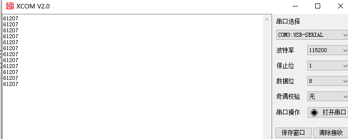
printf("%d\r\n",W25Q128_Read_ID());
delay_ms(1000);
}
}
(2) Effect
2. Page write and read function test
(1) Code
main.c code: (other codes are in II and 20)
#include "stm32f10x.h"
#include "spi.h"
#include "delay.h"
#include "usart.h"
#include "w25q128.h"
#include "led.h"
u8 read_buff[0XFFF];//Note that the size of this array should not be changed. It also serves the data backup of sector erasure
int main(void)
 {
	 u8 arr[256];
	 u16 i;
	 MySPI_Init();
	 delay_init();
	 LED_Init();
	 uart_init(115200);
	 for(i=0;i<256;i++)
		arr[i]=i+1;
	  PBout(5)=0;
	  PEout(5)=1;
	 while(1)
	 {
		  PBout(5)=!PBout(5);
	      PEout(5)=!PEout(5);
		 W25Q128_Write_page(0x000000,100,arr);
		 W25Q128_Read_Data(0x000000,50);			//Read data

		for(i=0;i<50;i++)
		printf("%d ",read_buff[i]);
		printf("\r\n ");
		delay_ms(1000);
	 }
 }
(2) Effect
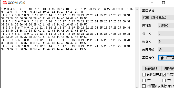
3. Full chip erase function test
(1) Code
main.c code: (other codes are in II and 20)
#include "stm32f10x.h"
#include "spi.h"
#include "delay.h"
#include "usart.h"
#include "w25q128.h"
#include "led.h"
u8 read_buff[0XFFF];//Note that the size of this array should not be changed. It also serves the data backup of sector erasure
int main(void)
 {
	 u8 arr[256];
	 u16 i;
	 MySPI_Init();
	 delay_init();
	 LED_Init();
	 uart_init(115200);
	 for(i=0;i<256;i++)
		arr[i]=i+1;
	  PBout(5)=0;
	  PEout(5)=1;
	 while(1)
	 {
		  PBout(5)=!PBout(5);
	      PEout(5)=!PEout(5);
		 W25Q128_Write_page(0x000000,100,arr);
		 W25Q128_Read_Data(0x000000,50);			//Read data

		for(i=0;i<50;i++)
		printf("%d ",read_buff[i]);
		printf("\r\n ");

		W25Q128_Chip_Erase();//Full erase

		W25Q128_Read_Data(0x000000,50);			//Read data
		for(i=0;i<50;i++)
		printf("%d ",read_buff[i]);
		printf("\r\n ");
		delay_ms(1000);
	 }
 }
(2) Effect
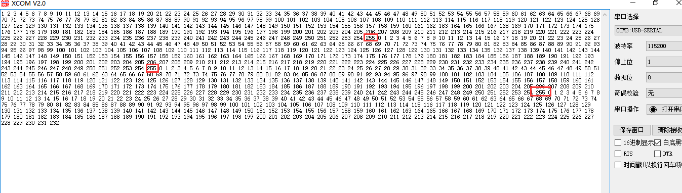
It can be seen that before erasing, write the number of 1 ~ 100, read the number of 1 ~ 50, and print it normally.
After the whole chip is erased, read the data again, and the data is 255, that is, all eight bits are 1.
4. Sector erase function test
(1) Code
main.c code: (other codes are in II and 20)
#include "stm32f10x.h"
#include "spi.h"
#include "delay.h"
#include "usart.h"
#include "w25q128.h"
#include "led.h"
u8 read_buff[0XFFF];//Note that the size of this array should not be changed. It also serves the data backup of sector erasure
int main(void)
{
u8 arr[256];
u16 i;
MySPI_Init();
delay_init();
LED_Init();
uart_init(115200);
for(i=0;i<256;i++)
arr[i]=i+1;
PBout(5)=0;
PEout(5)=1;
while(1)
{
PBout(5)=!PBout(5);
PEout(5)=!PEout(5);
W25Q128_Write_page(0x000000,100,arr);
W25Q128_Read_Data(0x000000,50); //Read data
for(i=0;i<50;i++)
printf("%d ",read_buff[i]);
printf("\r\n ");
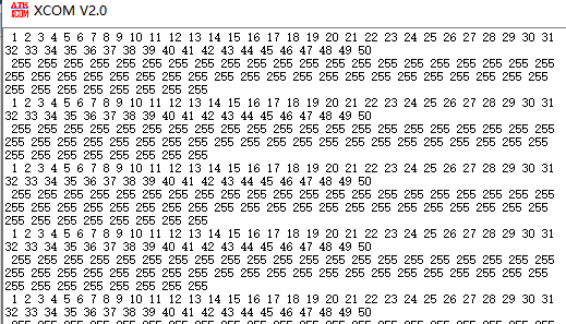
W25Q128_Sector_Erase(0x000000); //Sector Erase
W25Q128_Read_Data(0x000000,50); //Read data
for(i=0;i<50;i++)
printf("%d ",read_buff[i]);
printf("\r\n ");
delay_ms(1000);
}
}
(2) Effect
During the test, it is found that the full chip erase data is very long (should be greater than 10s), while the sector erase data is very short, and it is basically impossible to see that the erase sector statement is executed.
Change the address of the sector erase function:
W25Q128_Sector_Erase(0x000005); //Sector Erase
The test effect is the same as when the address is 0x000000. The address passed during the erasure of the visible sector is not necessarily the first address of the sector, but can be any address in a sector. During erasure, all sectors in which the address is located will be erased
5. Block erase test
(1) Code
main.c code: (other codes are in II and 20)
#include "stm32f10x.h"
#include "spi.h"
#include "delay.h"
#include "usart.h"
#include "w25q128.h"
#include "led.h"
u8 read_buff[0XFFF];//Note that the size of this array should not be changed. It also serves the data backup of sector erasure
int main(void)
{
u8 arr[256];
u16 i;
MySPI_Init();
delay_init();
LED_Init();
uart_init(115200);
for(i=0;i<256;i++)
arr[i]=i+1;
PBout(5)=0;
PEout(5)=1;
while(1)
{
PBout(5)=!PBout(5);
PEout(5)=!PEout(5);
W25Q128_Write_page(0x000000,100,arr);
W25Q128_Read_Data(0x000000,50); //Read data
for(i=0;i<50;i++)
printf("%d ",read_buff[i]);
printf("\r\n ");
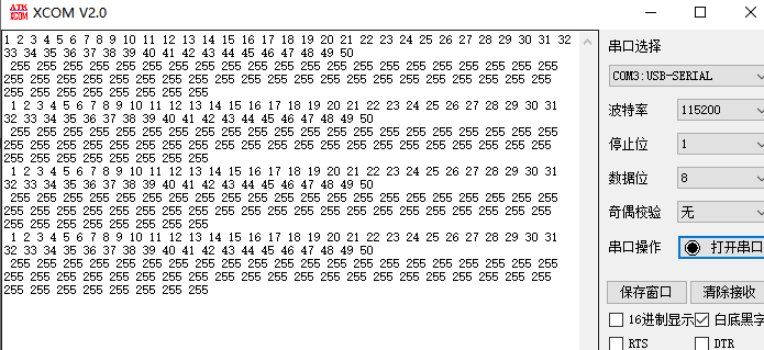
W25Q128_Block_Erase(0x000000); //Block erase
W25Q128_Read_Data(0x000000,50); //Read data
for(i=0;i<50;i++)
printf("%d ",read_buff[i]);
printf("\r\n ");
delay_ms(1000);
}
}
(2) Effect
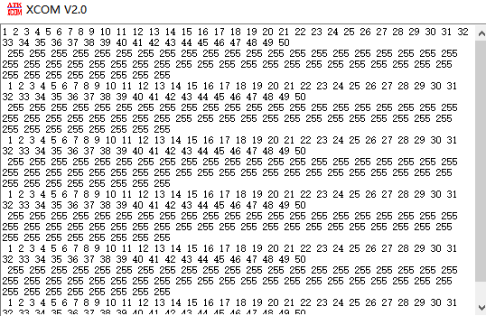
Change the address of the cross erase function:
W25Q128_Block_Erase(0x000005); //Block erase
The test effect is the same as when the address is 0x000000. It can be seen that the address passed during block division is not necessarily the first address of the block, but can be any address in a block. When erasing, all the blocks where the address is located will be erased
6. Sequential write function test
(1) Code
main.c code: (other codes are in II and 20)
#include "stm32f10x.h"
#include "spi.h"
#include "delay.h"
#include "usart.h"
#include "w25q128.h"
#include "led.h"
u8 read_buff[0XFFF];//Note that the size of this array should not be changed. It also serves the data backup of sector erasure
#define SIZE 1000
int main(void)
{
u8 arr[SIZE];
u16 i=0,j=1;
MySPI_Init();
delay_init();
LED_Init();
uart_init(115200);
//W25Q128_Chip_Erase();// Full erase
while(j<=SIZE)
{
arr[i++]=j%256;
j++;
}
PBout(5)=0;
PEout(5)=1;
while(1)
{
PBout(5)=!PBout(5);
PEout(5)=!PEout(5);
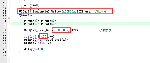
W25Q128_Sequential_Write(0x000000,SIZE,arr);//Sequential write
W25Q128_Read_Data(0x000000,SIZE); //Read data
for(i=0;i<SIZE;i++)
printf("%d ",read_buff[i]);
printf("\r\n ");
delay_ms(1000);
}
}
(2) Effect
You can see that 1000 numbers are written in, 1 ~ 255, 0 ~ 255, 0 ~ 255 and 0 ~ 232
The data read out is correct and fast. The function that moved the array before is written very slowly. We won't test that function here.
In order to verify that the page is not read cyclically, the write address and read address are not written as the page start address, and are modified as follows:
Retest:
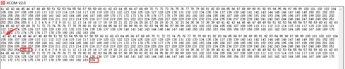
You can see that after reading this page, you can start reading from the next page. The output starts from 0. If you still start reading from the 0 address of this page, the subsequent output should be 255... 255
6. Sequential erase function test
(1) Cross sector erasure idea (+ an important note)
Because the minimum erasure unit of W25Q128 is sector, i.e. 4096B, one part of a group of data can be stored in a sector and the other part can be stored in the next sector. There are other data in the two sectors. After cross sector erasure, the data of the two sectors can be re output. Check whether only the data to be erased is erased.
There is an important thing: the maximum capacity of the global array defined by STM32 is 4095, which can be defined as u8 read_buff[0XFFF];, The local array in the called function has been tested. The maximum capacity is 1620. After that, the program will die (this number may vary from board to board?)
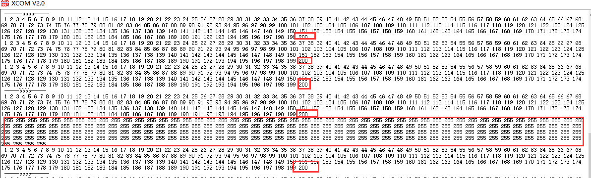
If the data of both sectors are output, the serial port monitoring page is not easy to screenshot. Take the number of 200 as an example.
At the beginning of the test program, input 200 numbers to the beginning of sector 17 (200 numbers from 0x010000 address) as the data that will not be erased in this sector.
Input 200 numbers into the 4080th address space (0x010ff0) of sector 17, then 16 numbers are stored in sector 17 and 284 numbers are stored in sector 18. These 200 numbers are used for erasure (sequential erasure across sectors).
Input 200 numbers to the 3840 address of sector 18, store the address to 4040, and return to sector 18. These 200 numbers are used as the data that will not be erased in sector 18.
After writing data, first read out the data, look at the data, then erase the 200 numbers stored in sectors 17 and 18, and then output the number of 600 address spaces to view on the serial port monitor
(2) Sector erase code
main.c code: (other codes are in II and 17)
#include "stm32f10x.h"
#include "spi.h"
#include "delay.h"
#include "usart.h"
#include "w25q128.h"
#include "led.h"

u8 read_buff[0XFFF];//Note that the size of this array should not be changed. It also serves the data backup of sector erasure

#define SIZE 200
int main(void)
 {
	 u8 arr[SIZE];
	 u16 i=0,j=1;
	 MySPI_Init();
	 delay_init();
	 LED_Init();
	 uart_init(115200);
	 //W25Q128_Chip_Erase();// Full erase
	 while(j<=SIZE)
	 {
		arr[i++]=j%256;
		j++;
	 }
	  PBout(5)=0;
	  PEout(5)=1;
	 W25Q128_Sequential_Write(0x010000,SIZE,arr);// Number of 200 start address writes in sector 17
	 W25Q128_Sequential_Write(0x010FF0,SIZE,arr);//Write 200 numbers to the 4080 address of sector 17 (erase the 200 numbers)
	 W25Q128_Sequential_Write(0x011F00,SIZE,arr);//Start to write 200 numbers at the 3840th address of sector 18

	 delay_ms(1000);
	 printf("\n\r------aaaa-----\r\n ");
	 W25Q128_Read_Data(0x010000,SIZE);			//Read the number of 200 start addresses written in sector 17
	 for(i=0;i<SIZE;i++)
	 printf("%d ",read_buff[i]);
	 printf("\r\n ");

	 W25Q128_Read_Data(0x010FF0,SIZE);			//Read the number of 200 written to the 4080 address of sector 17
	 for(i=0;i<SIZE;i++)
	 printf("%d ",read_buff[i]);
	 printf("\r\n ");

	 W25Q128_Read_Data(0x011F00,SIZE);			//Read the 3840th address of sector 18 and start writing 200 numbers
	 for(i=0;i<SIZE;i++)
	 printf("%d ",read_buff[i]);
	 printf("\r\n ");

	 printf("\n\r-----bbbb-----\r\n ");
	 W25Q128_Sequential_Erase(0x010FF0,SIZE);//Erase the number of 200 written to the 4080 address of sector 17
	 delay_ms(1000);
	 while(1)
	 {
		PBout(5)=!PBout(5);
	    PEout(5)=!PEout(5);

		W25Q128_Read_Data(0x010000,SIZE);			//Read the number of 200 start addresses written in sector 17
		 for(i=0;i<SIZE;i++)
		 printf("%d ",read_buff[i]);
		 printf("\r\n ");

		 W25Q128_Read_Data(0x010FF0,SIZE);			//Read the number of 200 written to the 4080 address of sector 17
		 for(i=0;i<SIZE;i++)
		 printf("%d ",read_buff[i]);
		 printf("\r\n ");

		 W25Q128_Read_Data(0x011F00,SIZE);			//Read the 3840th address of sector 18 and start writing 200 numbers
		 for(i=0;i<SIZE;i++)
		 printf("%d ",read_buff[i]);
		 printf("\r\n ");
		 printf("\n\r-----cccc------\r\n ");
		delay_ms(1000);
	 }
 }
(3) Cross sector erase test effect
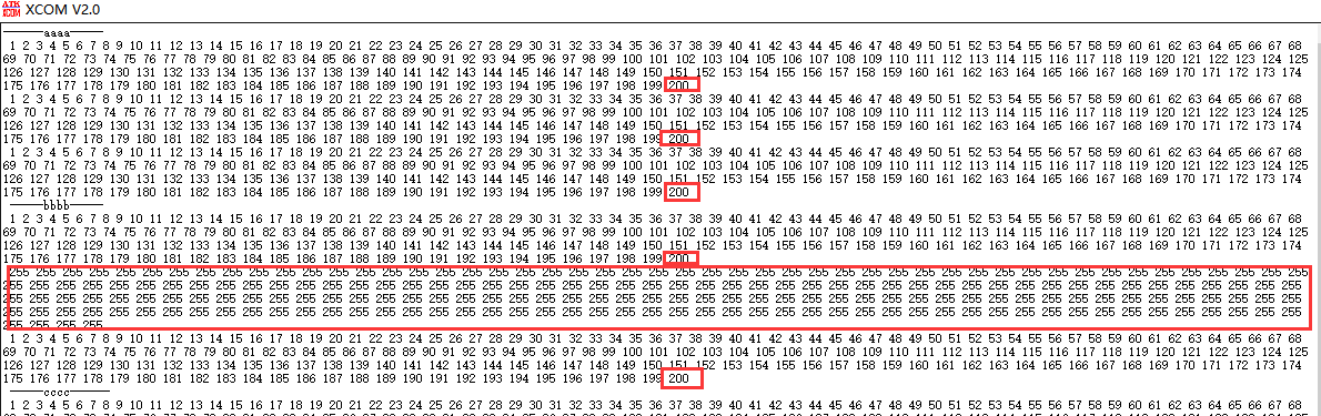
The above effect corresponds to the program
The output between the split line – aaaa –, -- bbbb – is the written data, and the output between – bbbb –, -- cccc – is the output of the 600 data after erasing 200 data across sectors.
It can be seen that the cross sector data is erased, and other data in the sector is not affected.
(4) Single sector erase code
main.c code: (other codes are in II and 17)
#include "stm32f10x.h"
#include "spi.h"
#include "delay.h"
#include "usart.h"
#include "w25q128.h"
#include "led.h"

u8 read_buff[0XFFF];//Note that the size of this array should not be changed. It also serves the data backup of sector erasure

#define SIZE 200
int main(void)
 {
	 u8 arr[SIZE];
	 u16 i=0,j=1;
	 MySPI_Init();
	 delay_init();
	 LED_Init();
	 uart_init(115200);
	 //W25Q128_Chip_Erase();// Full erase

	 while(j<=SIZE)
	 {
		arr[i++]=j%256;
		j++;
	 }
	  PBout(5)=0;
	  PEout(5)=1;
	 W25Q128_Sequential_Write(0x000000,SIZE,arr);//Number of 200 start address writes in sector 1
	 W25Q128_Sequential_Write(0x0003E8,SIZE,arr);//Write 200 numbers at the 1000th address of sector 1 (erase the 200 numbers)
	 W25Q128_Sequential_Write(0x000BB8,SIZE,arr);//Start to write 200 numbers at the 3000th address of sector 1

	 delay_ms(1000);
	 printf("\n\r------aaaa-----\r\n ");
	 W25Q128_Read_Data(0x010000,SIZE);			//Read the 200 numbers written to the start address of sector 1
	 for(i=0;i<SIZE;i++)
	 printf("%d ",read_buff[i]);
	 printf("\r\n ");

	 W25Q128_Read_Data(0x0003E8,SIZE);			//Read the number of 200 written to the 1000th address of sector 1
	 for(i=0;i<SIZE;i++)
	 printf("%d ",read_buff[i]);
	 printf("\r\n ");

	 W25Q128_Read_Data(0x000BB8,SIZE);			//Read the 3000th address of sector 1 and start writing 200 numbers
	 for(i=0;i<SIZE;i++)
	 printf("%d ",read_buff[i]);
	 printf("\r\n ");

	 printf("\n\r-----bbbb-----\r\n ");
	 W25Q128_Sequential_Erase(0x0003E8,SIZE);	//Erase the number of 200 written to the 1000th address of sector 1
	 delay_ms(1000);
	 while(1)
	 {
		PBout(5)=!PBout(5);
	    PEout(5)=!PEout(5);

		W25Q128_Read_Data(0x010000,SIZE);			//Read the 200 numbers written to the start address of sector 1
		 for(i=0;i<SIZE;i++)
		 printf("%d ",read_buff[i]);
		 printf("\r\n ");

		 W25Q128_Read_Data(0x0003E8,SIZE);			//Read the number of 200 written to the 1000th address of sector 1
		 for(i=0;i<SIZE;i++)
		 printf("%d ",read_buff[i]);
		 printf("\r\n ");

		 W25Q128_Read_Data(0x000BB8,SIZE);			//Read the 3000th address of sector 1 and start writing 200 numbers
		 for(i=0;i<SIZE;i++)
		 printf("%d ",read_buff[i]);
		 printf("\r\n ");

		 printf("\n\r-----cccc------\r\n ");
		delay_ms(1000);
	 }
 }
(5) Single sector erase test effect
You can see that the 200 numbers of the second input are erased, and the output is 255, while the data in other places is still retained.