What I bring to you today is mastering FPGA VHDL Day 6 in a week. Today, I open the sixth day to bring VHDL simulation. Let's stop talking nonsense. Let's have a look. Ten minutes a day. Keep going. Quantity becomes quality.
VHDL language
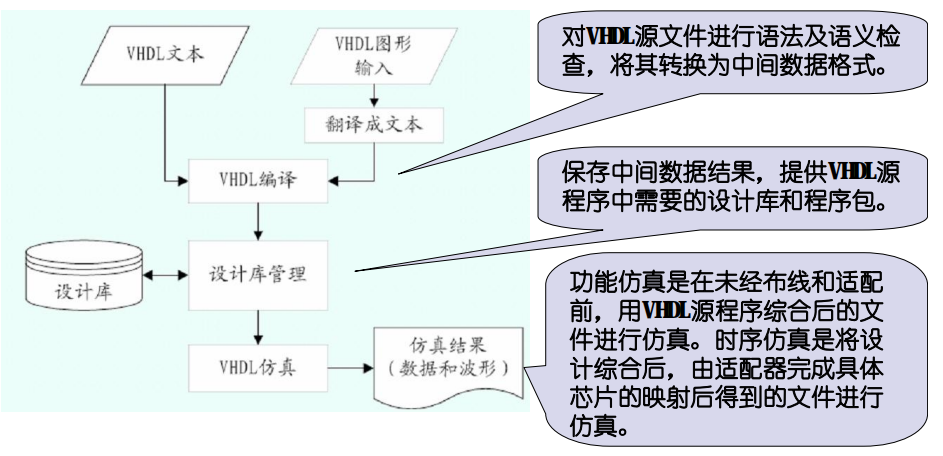
6, VHDL simulation
Simulation (also known as simulation), does not touch the specific hardware system to use the computer to simulate and test the logic behavior and operation function of circuit design. The final completion of large-scale VHDL system design must go through the multi-level simulation and test process, including VHDL behavior simulation for the system, time sequence simulation and hardware simulation by modules, until the final system level simulation Hardware simulation test.
6.1 generation of simulation excitation signal
LIBRARY IEEE;USE IEEE.STD_LOGIC_1164.ALL;ENTITY ADDER4 ISPORT ( a, b : IN INTEGER RANGE 0 TO 15;c : OUT INTEGER RANGE 0 TO 15 );END ADDER4;ARCHITECTURE one OF ADDER4 ISBEGINc <= a + b;END one;
Method 1:
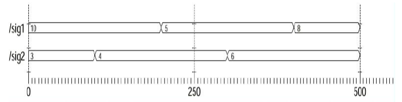
① Write a waveform signal generator with VHDL
ENTITY SIGGEN ISPORT ( sig1 : OUT INTEGER RANGE 0 TO 15;sig2 : OUT INTEGER RANGE 0 TO 15 );END;ARCHITECTURE Sim OF SIGGEN ISBEGINsig1 <= 10, 5 AFTER 200 ns, 8 AFTER 400 ns;sig2 <= 3, 4 AFTER 100 ns, 6 AFTER 300 ns;END;
SIGGEN simulation output waveform:
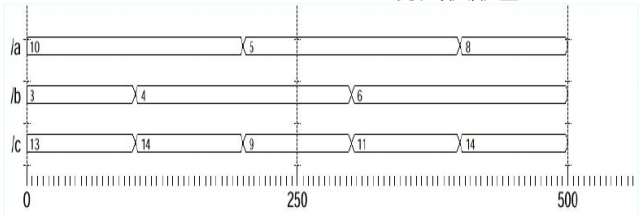
② The waveform signal generator and ADDER4 are assembled into a VHDL simulation test module
ENTITY BENCH ISEND;ARCHITECTURE one OF BENCH ISCOMPONENT ADDER4PORT ( a, b : integer range 0 to 15;c : OUT INTEGER RANGE 0 TO 15 );END COMPONENT;COMPONENT SIGGENPORT ( sig1 : OUT INTEGER RANGE 0 TO 15;sig2 : OUT INTEGER RANGE 0 TO 15 );END COMPONENT;SIGNAL a, b, c : INTEGER RANGE 0 TO 15;BEGINU1 : ADDER4 PORT MAP (a, b, c);U2 : SIGGEN PORT MAP (sig1=>a, sig2=>b);END;
SIGGEN simulation output waveform:
-
Using waveform setting command of simulator to apply excitation signal
The format of the force command is as follows: force < signal name > < value > [< time >] [, < value > < time > ][- repeat < cycle >]
force a 0 (the current value of the forcing signal is 0) force b 0 0, 1 10 (the value of the forcing signal B at time 0 is 0, the value of the forcing signal B at time 10 is 1) force clk 0 0, 1 15 – repeat 20 (clk is the periodic signal, the period is 20)
The structure of ADDER4 is simulated
① After initializing the simulation process, enter the command at the command line:
force a 10 0, 5 200, 8 400force b 3 0, 4 100, 6 300
SIGGEN simulation output waveform:
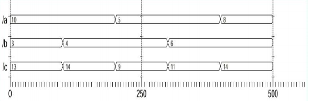
② Execute the RUN command.
6.2 VHDL Test Bench
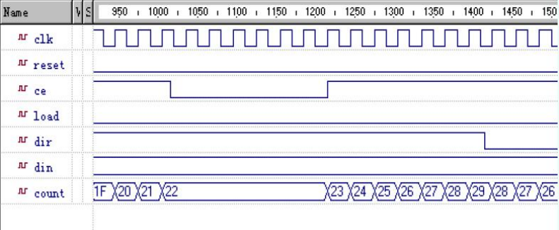
8-bit counter source program:
Library IEEE;use IEEE.std_logic_1164.all;entity counter8 isport (CLK, CE, LOAD, DIR, RESET: in STD_LOGIC;DIN: in INTEGER range 0 to 255;COUNT: out INTEGER range 0 to 255 );end counter8;architecture counter8_arch of counter8 isbeginprocess (CLK, RESET)variable COUNTER: INTEGER range 0 to 255;beginif RESET='1' then COUNTER := 0;elsif CLK='1' and CLK'event thenif LOAD='1' then COUNTER := DIN;Elseif CE='1' thenif DIR='1' thenif COUNTER =255 then COUNTER := 0;else COUNTER := COUNTER + 1;end if;elseif COUNTER =0 then COUNTER := 255;else COUNTER := COUNTER-1;end if;end if;end if;end if;end if;COUNT <= COUNTER;end process;end counter8_arch;
Test Bench:
Entity testbench is end testbench;Architecture testbench_arch of testbench isFile RESULTS: TEXT open WRITE_MODE is "results.txt";Component counter8port ( CLK: in STD_LOGIC;RESET: in STD_LOGIC;CE, LOAD, DIR: in STD_LOGIC;DIN: in INTEGER range 0 to 255;COUNT: out INTEGER range 0 to 255 );end component;shared variable end_sim : BOOLEAN := false;signal CLK, RESET, CE, LOAD, DIR: STD_LOGIC;signal DIN: INTEGER range 0 to 255;signal COUNT: INTEGER range 0 to 255;procedure WRITE_RESULTS (CLK,CE,LOAD,LOAD,RESET : STD_LOGIC;DIN,COUNT : INTEGER ) isVariable V_OUT : LINE;Beginwrite(V_OUT, now, right, 16, ps); -- Enter timewrite(V_OUT, CLK, right, 2);write(V_OUT, RESET, right, 2);write(V_OUT, CE, right, 2);write(V_OUT, LOAD, right, 2);write(V_OUT, DIR, right, 2);write(V_OUT, DIN, right, 257);--write outputswrite(V_OUT, COUNT, right, 257);writeline(RESULTS,V_OUT);end WRITE_RESULTS;beginUUT: COUNTER8port map (CLK => CLK,RESET => RESET,CE => CE, LOAD => LOAD,DIR => DIR, DIN => DIN,COUNT => COUNT );CLK_IN: processBeginif end_sim = false then CLK <= '0';Wait for 15 ns;CLk <='1';Wait for 15 ns;ElseWait;end if;end process;STIMULUS: processBeginRESET <= '1';CE <= '1'; --Count enableDIR <= '1'; -- Add countDIN <= 250; -- input data LOAD <= '0'; --Disable loading of input data wait for 15 ns;RESET <= '0';wait for 1 us;CE <= '0'; --No counting pulse signal wait for 200 ns;CE <= '1';wait for 200 ns;DIR <= '0';wait for 500 ns;LOAD <= '1';wait for 60 ns;LOAD <= '0';wait for 500 ns;DIN <= 60;DIR <= '1';LOAD <= '1';wait for 60 ns;LOAD <= '0';wait for 1 us;CE <= '0';wait for 500 ns;CE <= '1';wait for 500 ns;end_sim :=true;wait;end process;WRITE_TO_FILE: WRITE_RESULTS(CLK,RESET,CE,LOAD,DIR,DIN,COUNT);End testbench_arch;
Waveform of 8-bit counter test reference simulation part:
Day 6 is here, and Day 7 will bring the last one, VHDL synthesis.