Analysis of errors in AFIO clock
AFIO misunderstanding
We generally misunderstand it as "enabling the multiplexing function of the IO port requires enabling the AFIO clock", but let's recall the structure diagram of GPIO and learn more about GPIOx_Pin structure:
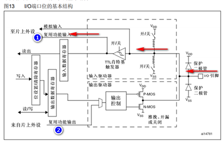
In the figure above, the signal from the port pin enters the multiplexing input channel, and we can see that the signal flowing into the ordinary GPIO input channel can also flow into the multiplexing function input channel, This indicates that "the internal and external devices connected to the pin multiplexing input channel (the internal and external devices are devices such as IIC) can receive the input signal of the pin without AFIO clock".
Why not use AFIO for multiplexing function?
We also know a term called "multiplexing function". The multiplexing function is different from port remapping. The multiplexing function is "the internal and external devices directly connected to the multiplexing input and output channels in the above figure". We only need to configure the output mode as the multiplexing output mode and the input mode as the input mode corresponding to the requirements of the internal and external devices (floating, up and down), At this point, our internal and external input and output channels are configured.
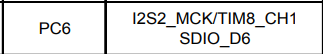
The multiplexing function is essentially different from port remapping. Pin multiplexing is the inherent function of this pin. We know that a pin has many functions, as shown in the following table: PC6 can also be used as i2s2 in addition to the normal GPIO function_ MCK or TIM8_CH1 or SDIO_D6 use.
However, after the port is remapped, a peripheral function of the original pin is migrated to other pins, and the peripheral function of the original pin fails.
What is the magical effect of AFIO?
You know the difference between reuse and remapping, but do you know how the function of this pin is migrated? Do not think that the wiring line of the pin is changed, but AFIO works. Due to the multiplexing IO clock enable, the input and output signals originally belonging to the original pin are guided to the positions ① and ② of the remapping pin through other internal channels as new input and output pins. At this point, we can regard AFIO as a signal migration personnel. When we need to "accept the pin signal read by the ① channel at the position not directly connected with the ① position", or when we need to "introduce the signal at the position not directly connected with the ② channel into the ② channel for output", we must use the signal Porter AFIO.
The places where signal porters (AFIO) are needed are mainly "the signal sending source is not directly connected with the multiplexed output channel" or "the signal receiving source is not directly connected with the multiplexed input channel":
① Need to enable AFIO clock when port pin remapping?

For example, for the remapping of TIM1 pin above, we know TIM1_CH1 original pin should be PA8:
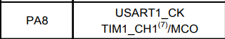
At this time, I mentioned earlier that "if a medium is needed to transfer the input and output signal of PA8 to the input and output signal of PE9, this medium is AFIO", then the AFIO clock must be provided at this time.
② When the peripherals we use are not on the APB2 bus, we need to act as a signal relay through AFIO.
For example, when we output PWM, we usually use TIM2 and TIM3 on APB1 bus, and rarely use TIM1 and TIM8 on APB2 bus. When we use the internal and external functions on the non APB2 bus, because the input and output signals on different buses cannot be directly transmitted to each other, a signal Porter is needed to make the pulse signals on different buses transmit correctly, so that the pulse signals will not be disordered under different driving clocks. For example, the following code snippet:
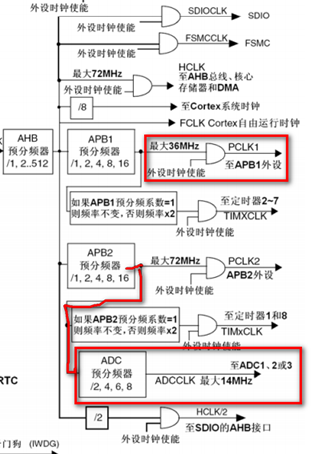
When TIM3 connected to APB1 bus outputs PWM, it is necessary to enable AFIO clock:
void TIM3_PWM_Init(u16 arr,u16 psc)
{
 GPIO_InitTypeDef GPIO_InitStructure;
 TIM_TimeBaseInitTypeDef  TIM_TimeBaseStructure;
 TIM_OCInitTypeDef  TIM_OCInitStructure;

 RCC_APB1PeriphClockCmd(RCC_APB1Periph_TIM3, ENABLE); //Enable timer 3 clock
  RCC_APB2PeriphClockCmd(RCC_APB2Periph_GPIOB  | RCC_APB2Periph_AFIO, ENABLE);  //Enable GPIO peripheral and AFIO multiplexing function module clock

 GPIO_PinRemapConfig(GPIO_PartialRemap_TIM3, ENABLE); //Timer3 partial remapping} tim3_ CH2->PB5

   //Set this pin as the multiplexing output function and output the PWM pulse waveform of TIM3 ^ CH2 ^ gpiob five
 GPIO_InitStructure.GPIO_Pin = GPIO_Pin_5; //TIM_CH2
 GPIO_InitStructure.GPIO_Mode = GPIO_Mode_AF_PP;  //Multiplex push-pull output
 GPIO_InitStructure.GPIO_Speed = GPIO_Speed_50MHz;
 GPIO_Init(GPIOB, &GPIO_InitStructure);//Initialize GPIO

   //Initialize TIM3
 TIM_TimeBaseStructure.TIM_Period = arr; //Sets the value of the auto reload register cycle of the load activity at the next update event
 TIM_TimeBaseStructure.TIM_Prescaler =psc; //Sets the prescaled value used as the divisor of TIMx clock frequency
 TIM_TimeBaseStructure.TIM_ClockDivision = 0; //Set clock division: TDTS = Tck_tim
 TIM_TimeBaseStructure.TIM_CounterMode = TIM_CounterMode_Up;  //TIM up count mode
 TIM_TimeBaseInit(TIM3, &TIM_TimeBaseStructure); //According to Tim_ The parameter specified in timebaseinitstruct initializes the time base unit of TIMx

 //Initialize TIM3 # Channel2 # PWM mode
 TIM_OCInitStructure.TIM_OCMode = TIM_OCMode_PWM2; //Select timer mode: TIM pulse width modulation mode 2
  TIM_OCInitStructure.TIM_OutputState = TIM_OutputState_Enable; //Compare output enable
 TIM_OCInitStructure.TIM_OCPolarity = TIM_OCPolarity_High; //Output polarity: TIM output has high polarity
 TIM_OC2Init(TIM3, &TIM_OCInitStructure);  //Initialize the peripheral TIM3 # OC2 according to the parameters specified by T

 TIM_OC2PreloadConfig(TIM3, TIM_OCPreload_Enable);  //Enable TIM3 preload register on CCR2

 TIM_Cmd(TIM3, ENABLE);  //Enable TIM3
}
ADC analog-to-digital conversion connected to APB2 bus does not need to enable AFIO clock:
void  Adc_Init(void)
{
 ADC_InitTypeDef ADC_InitStructure;
 GPIO_InitTypeDef GPIO_InitStructure;

 RCC_APB2PeriphClockCmd(RCC_APB2Periph_GPIOA |RCC_APB2Periph_ADC1 , ENABLE );   //Enable ADC1 channel clock


 RCC_ADCCLKConfig(RCC_PCLK2_Div6);   //Set ADC frequency division factor 6 # 72m / 6 = 12, and the maximum ADC time cannot exceed 14M

 //PA1 # as analog channel input pin
 GPIO_InitStructure.GPIO_Pin = GPIO_Pin_1;
 GPIO_InitStructure.GPIO_Mode = GPIO_Mode_AIN;  //Analog input pin
 GPIO_Init(GPIOA, &GPIO_InitStructure);

 ADC_DeInit(ADC1);  //Reset ADC1 and reset all registers of the peripheral ADC1 to the default value

 ADC_InitStructure.ADC_Mode = ADC_Mode_Independent; //ADC working mode: ADC1 and ADC2 work in independent mode
 ADC_InitStructure.ADC_ScanConvMode = DISABLE; //Analog to digital conversion works in single channel mode
 ADC_InitStructure.ADC_ContinuousConvMode = DISABLE; //Analog to digital conversion works in single conversion mode
 ADC_InitStructure.ADC_ExternalTrigConv = ADC_ExternalTrigConv_None; //The conversion is initiated by software rather than an external trigger
 ADC_InitStructure.ADC_DataAlign = ADC_DataAlign_Right; //ADC data right alignment
 ADC_InitStructure.ADC_NbrOfChannel = 1; //The number of ADC channels that perform rule conversion sequentially
 ADC_Init(ADC1, &ADC_InitStructure); //According to ADC_ The parameter specified in initstruct initializes the register of the peripheral ADCx


 ADC_Cmd(ADC1, ENABLE); //Enables the specified ADC1

 ADC_ResetCalibration(ADC1); //Enable reset calibration

 while(ADC_GetResetCalibrationStatus(ADC1)); //Wait until reset calibration is complete

 ADC_StartCalibration(ADC1);  //Turn on AD calibration

 while(ADC_GetCalibrationStatus(ADC1));  //Wait until calibration is complete

// ADC_SoftwareStartConvCmd(ADC1, ENABLE); / / enable the software conversion startup function of the specified ADC1

}
③ Exi external interrupt line mapping needs to enable AFIO clock:
EXTI interrupt line is not directly connected with GPIO multiplex input channel. Some people wonder why EXTI does not have a dedicated clock? This is because EXTI is not an external device, but a "signal transmission medium" used to detect external level changes, which is equivalent to "processing the input signal and then transmitting the processed signal to the NVIC interrupt judgment priority controller".
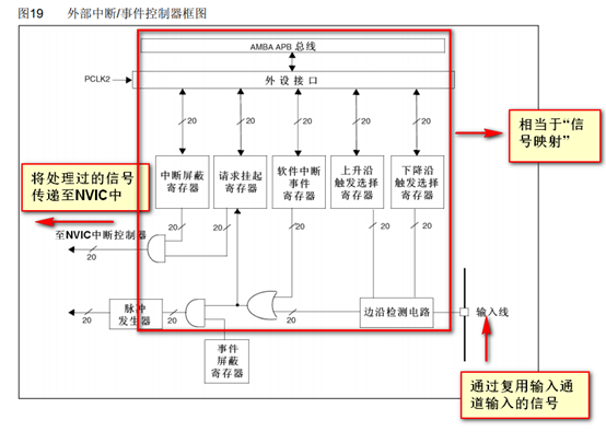
From the above figure, we can know that the signal transmission medium, that is, the signal Porter, is served by AFIO. Here is no exception. EXTI is equivalent to an AFIO function that maps the GPIO pin signal to the NVIC. Since EXTI acts as the signal mapping medium, the clock of EXTI is provided by AFIO. EXTI clock configuration example:
//GPIOx pin external interrupt attribute configuration
void GPIO_EXTI_Config()
{
    EXTI_InitTypeDef EXTI_InitStructure;

    //Configure multiplex IO clock
    RCC_APB2PeriphClockCmd(RCC_APB2Periph_AFIO,ENABLE);
    //Broken line mapping
    GPIO_EXTILineConfig(GPIO_PortSourceGPIOA,GPIO_PinSource8); //Select PA8 to map to broken wire in EXTI8
    GPIO_EXTILineConfig(GPIO_PortSourceGPIOC,GPIO_PinSource13); //Select PC13 to map to broken wire in EXTI13
    GPIO_EXTILineConfig(GPIO_PortSourceGPIOD,GPIO_PinSource0|GPIO_PinSource4); //Select PD0 and PD4 to map to EXTI0 and EXTI4 respectively
    //The up, down and left buttons are in the pull-down state when they are not triggered
    EXTI_InitStructure.EXTI_Line = EXTI_Line0|EXTI_Line4|EXTI_Line8;
    EXTI_InitStructure.EXTI_LineCmd = ENABLE; //Interrupt mask position bit
    EXTI_InitStructure.EXTI_Mode = EXTI_Mode_Interrupt;
    EXTI_InitStructure.EXTI_Trigger = EXTI_Trigger_Rising;
    EXTI_Init(&EXTI_InitStructure);
    //The temp key is in the pull-up state when it is not triggered
    EXTI_InitStructure.EXTI_Line = EXTI_Line13;
    EXTI_InitStructure.EXTI_LineCmd = ENABLE; //Interrupt mask position bit
    EXTI_InitStructure.EXTI_Mode = EXTI_Mode_Interrupt;
    EXTI_InitStructure.EXTI_Trigger = EXTI_Trigger_Falling;
    EXTI_Init(&EXTI_InitStructure);
}
Why is AFIO clock on APB2 bus?
Because we found that after the port remapping, the mapped new pins are GPIO pins, and GPIOx is the peripheral of APB2. As an active signal Porter, AFIO is suitable to use APB2 to provide it with a clock.