MSP430F5529 LaunchPad™ Development Kit
(MSP‑EXP430F5529LP)
Hard knowledge
1, MSP430 MCU port overview
General I/O port is the most important and commonly used peripheral module of MSP430 single chip microcomputer. The general I/O port can not only be directly used for input / output, but also provide necessary logic control signals for MSP430 MCU application system.
MSP430F5xx/6xx Series MCU can provide up to 12 general I/O ports (P1 ~ P11 and PJ). Most ports have 8 pins, and the number of pins of a few ports is less than 8. Each I/O pin can be independently set as an input or output pin, and each I/O pin can be independently read or written, and all port registers can be independently set or cleared.
P1 and P2 pins have interrupt capability. Interrupts introduced from each I/O pin of P1 and P2 ports can be enabled independently and set to trigger interrupts on the rising or falling edge. The I/O pins of all P1 ports are interrupted from the same interrupt vector P1IV. Similarly, the interrupt source of P2 port comes from another interrupt vector P2IV.
Each independent port can be byte accessed, or the two can be combined for word access. Port combinations P1 and P2, P3 and P4, P5 and P6, P7 and P8 can be combined as PA, PB, PC and PD ports. When the word operation is written to the PA port, all 16 bit data are written to this port; When the low byte of PA port is written by byte operation, the high byte remains unchanged; When the high byte of PA port is written with byte instruction, the low byte remains unchanged. The same is true for other ports. When the length of the written data is less than the maximum length of the port, the unused bits remain unchanged. Apply this rule to access all ports, except interrupt vector registers P1IV and P2IV, which can only perform byte operations.
2, General IO port output characteristics
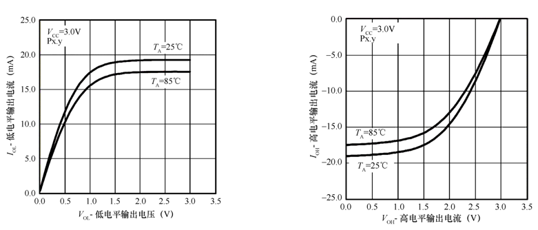
Under the condition of default output drive (PxDS.y=0, i.e. under drive strength) and MCU power supply voltage VCC of 3V, the output characteristics of port low level and high level are shown in the following two figures respectively, in which the current input is positive and the output is negative.
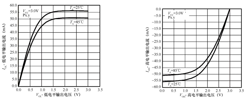
When pxds When the y control bit is configured as 1, that is, the MCU port is configured as strong drive mode. In the strong drive mode, the low-level and high-level output characteristics of the port are shown in the following two figures respectively.
3, Ports P1 and P2
Ports P1 and P2 have input / output, interrupt and external module functions, which can be realized by setting their respective 9 control registers. P1 and P2 are described below.
1. Input register PxIN
The input register is a read-only register for the CPU to scan the I/O pin signal. The user cannot write to it. The input signal of the I/O port can only be obtained by reading the contents of the register. At this time, the direction of the pin must be selected as the input. A bit in the input register is 0, indicating that the bit input is low; A bit of 1 indicates that the bit input is high.
2. Output register PxOUT
This register is the output buffer register of the I/O port. Its contents can be written like operating memory data to change the output state of I/O port. When reading, the contents of the output cache are independent of the pin direction definition. Changing the contents of the direction register will not affect the contents of the output cache.
0: output is low; 1: The output is high.
3. Direction register PxDIR
The independent 8 bits define the input / output direction of the 8 pins respectively. 8 bits are reset after PUC. When using the input or output function, the direction of the port should be defined first, and the input / output can meet the requirements of the designer. As input, it can only be read; As output, it is readable and writable.
0: input mode; 1: Output mode.
4. Pull up / pull down resistance enable register PxREN
Each bit of the register can enable the pull-up / pull-down resistance of the corresponding I/O pin. The register needs to be used with the output register to complete the configuration of pull-up / pull-down resistance.
0: pull-up / pull-down resistance is prohibited; 1: Pull up / pull down resistance enable.
5. Output drive capability adjustment register PxDS
Each bit of the PxDS register enables the relevant pin to select full drive mode and secondary drive mode (reduce drive capability). The default is secondary drive mode.
0: secondary drive mode; 1: Full drive mode.
6. Function selection register PxSEL
P1 and P2 ports also have other on-chip and off-chip functions. In order to reduce pins, these functions are connected outside the chip by multiplexing P1 and P2 pins. PxSEL is used to select the I/O port function and peripheral module function of the pin.
0: select pin for common I/O function; 1: Select pin for peripheral module function.
7. Interrupt enable register PxIE
The 8 bits of the register correspond to the 8 pins of the port one by one, and each bit is used to control the interrupt permission of the corresponding pin.
8. Interrupt trigger edge selection register PxIES
If a pin of Px port is allowed to interrupt, it is also necessary to define the interrupt trigger edge of this pin. The 8 bits of the register define the interrupt trigger edges of the 8 pins of the Px port respectively.
9. Interrupt flag register PxIFG
The register has 8 flag bits, which contain information about whether the corresponding pin has an interrupt to be processed, that is, whether the corresponding pin has an interrupt request. If a pin of Px allows interrupt and the rising edge is selected, when the pin jumps from low level to high level, the corresponding bit of PxIFG will be set, indicating that an interrupt event has occurred on the pin.
4, Port P3~P11
These ports have no interrupt capability, and other functions are the same as P1 and P2 ports, which can realize input / output functions and peripheral module functions. Each port has 6 registers for users to use. Users can access and control them through these 6 registers. The six registers of each port are: input register (PxIN), output register (PxOUT), direction selection register (PxDIR), output drive capability adjustment register (PxDS), pull-up / pull-down resistance enable register (PxREN) and function selection register (PxSEL). The specific usage is the same as P1 and P2 ports.
5, Port application
Port is the most frequently used peripheral resource in MCU. Generally, the port is configured in the initialization phase of the program. When configuring, first configure the function selection register PxSEL. If it is an I/O port function, continue to configure the direction register PxDIR; If it is an input, continue to configure the interrupt enable register PxIE; If interrupt is allowed, continue to configure interrupt trigger edge selection register PxIES.
It should be noted that the interrupts of P1 and P2 ports are multi-source interrupts, that is, the 8 bits of P1 port share an interrupt vector P1IV, and the 8 bits of P2 port also share an interrupt vector P2IV. When any of the 8 pins on Px port is triggered by an interrupt, it will enter the same interrupt service program. In the interrupt service program, first determine which pin triggered the interrupt through PxIFG, then execute the corresponding program, and finally clear the corresponding PxIFG flag bit with software.
GPIO API
GPIO APl is divided into three groups of functions:
Handle the function of configuring GPIO pin,
The ability to handle interrupts,
And the function of accessing pin values.
GPIO pin configuration
GPIO_setAsOutputPin(uint8_t selectedPort, uint16_t selectedPins);
GPIO_setAsInputPin(uint8_t selectedPort, uint16_t selectedPins);
GPIO_setAsInputPinWithPullDownResistor(uint8_t selectedPort, uint16_t selectedPins);
GPIO_setAsInputPinWithPullUpResistor(uint8_t selectedPort, uint16_t selectedPins);
GPIO_setDriveStrength(uint8_t selectedPort, uint16_t selectedPins, uint8_t
driveStrength);
GPIO_setAsPeripheralModuleFunctionOutputPin(uint8_t selectedPort, uint16_t
selectedPins);
GPIO_setAsPeripheralModuleFunctionInputPin(uint8_t selectedPort, uint16_t
selectedPins);
selectedPort
//is the selected port. Valid values are:
GPIO_PORT_P1
GPIO_PORT_P2
GPIO_PORT_P3
GPIO_PORT_P4
GPIO_PORT_P5
GPIO_PORT_P6
GPIO_PORT_P7
GPIO_PORT_P8
GPIO_PORT_P9
GPIO_PORT_P10
GPIO_PORT_P11
GPIO_PORT_PA
GPIO_PORT_PB
GPIO_PORT_PC
GPIO_PORT_PD
GPIO_PORT_PE
GPIO_PORT_PF
GPIO_PORT_PJ
selectedPins
/*
is the specified pin in the selected port. Mask value is the logical OR of any of
the following:
*/
GPIO_PIN0
GPIO_PIN1
GPIO_PIN2
GPIO_PIN3
GPIO_PIN4
GPIO_PIN5
GPIO_PIN6
GPIO_PIN7
GPIO_PIN8
GPIO_PIN9
GPIO_PIN10
GPIO_PIN11
GPIO_PIN12
GPIO_PIN13
GPIO_PIN14
GPIO_PIN15
GPIO_PIN_ALL8
GPIO_PIN_ALL16
driveStrength
//specifies the drive strength of the pin Valid values are:
GPIO_REDUCED_OUTPUT_DRIVE_STRENGTH
GPIO_FULL_OUTPUT_DRIVE_STRENGTH
Handling GPIO interrupts
GPIO_enableInterrupt(uint8_t selectedPort, uint16_t selectedPins);
GPIO_disableInterrupt(uint8_t selectedPort, uint16_t selectedPins);
GPIO_clearInterrupt(uint8_t selectedPort, uint16_t selectedPins);
GPIO_getInterruptStatus(uint8_t selectedPort, uint16_t selectedPins);
GPIO_selectInterruptEdge(uint8_t selectedPort, uint16_t selectedPins, uint8_t
edgeSelect);
edgeSelect
//specifies what transition sets the interrupt flag Valid values are:
GPIO_HIGH_TO_LOW_TRANSITION
GPIO_LOW_TO_HIGH_TRANSITION
Access GPIO Pin value
GPIO_setOutputHighOnPin(uint8_t selectedPort, uint16_t selectedPins);
GPIO_setOutputLowOnPin(uint8_t selectedPort, uint16_t selectedPins);
GPIO_toggleOutputOnPin(uint8_t selectedPort, uint16_t selectedPins);
GPIO_getInputPinValue(uint8_t selectedPort, uint16_t selectedPins);
Actual combat
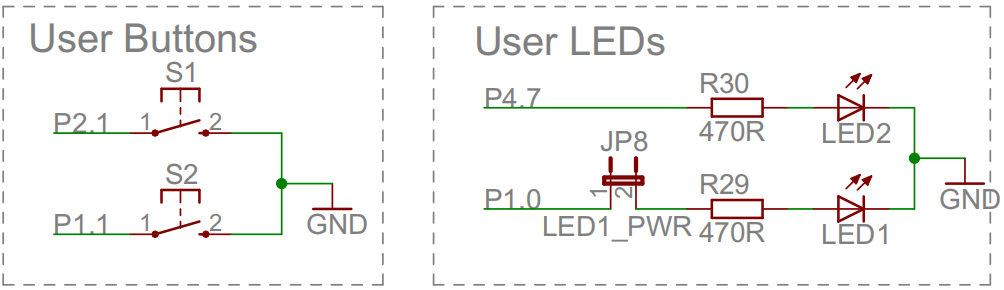
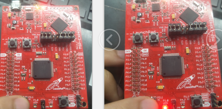
The user key is P2 1,P1.1. LED is P4 7,P1.0
Place P2 1 is set as the internal pull-up input, P1 0 is set as output. When S1 is pressed, LED1 is reversed
    GPIO_setAsInputPinWithPullUpResistor(GPIO_PORT_P2, GPIO_PIN1);
    GPIO_setAsOutputPin(GPIO_PORT_P1, GPIO_PIN0);

    while(1)
    {
        if(!GPIO_getInputPinValue(GPIO_PORT_P2, GPIO_PIN1))
        {
            delay_ms(20);
            if(!GPIO_getInputPinValue(GPIO_PORT_P2, GPIO_PIN1))
            {
                GPIO_toggleOutputOnPin(GPIO_PORT_P1, GPIO_PIN0);
                while(!GPIO_getInputPinValue(GPIO_PORT_P2, GPIO_PIN1));
            }
        }
    }
The whole main file is
#include "driverlib.h"

#define MCLK_IN_HZ      25000000

#define delay_us(x)     __delay_cycles((MCLK_IN_HZ/1000000*(x)))
#define delay_ms(x)     __delay_cycles((MCLK_IN_HZ/1000*(x)))

int main(void)
{
    WDT_A_hold(WDT_A_BASE);

    GPIO_setAsPeripheralModuleFunctionInputPin(GPIO_PORT_P5, GPIO_PIN2);
    GPIO_setAsPeripheralModuleFunctionOutputPin(GPIO_PORT_P5, GPIO_PIN3);

    UCS_turnOnXT2 (UCS_XT2_DRIVE_4MHZ_8MHZ);

    PMM_setVCore(PMM_CORE_LEVEL_3);

    UCS_initClockSignal(UCS_FLLREF, UCS_XT2CLK_SELECT, UCS_CLOCK_DIVIDER_8);
    UCS_initFLLSettle(25000, 50);

    UCS_initClockSignal(UCS_MCLK, UCS_DCOCLK_SELECT, UCS_CLOCK_DIVIDER_1);

    GPIO_setAsInputPinWithPullUpResistor(GPIO_PORT_P2, GPIO_PIN1);
    GPIO_setAsOutputPin(GPIO_PORT_P1, GPIO_PIN0);

    while(1)
    {
        if(!GPIO_getInputPinValue(GPIO_PORT_P2, GPIO_PIN1))
        {
            delay_ms(20);
            if(!GPIO_getInputPinValue(GPIO_PORT_P2, GPIO_PIN1))
            {
                GPIO_toggleOutputOnPin(GPIO_PORT_P1, GPIO_PIN0);
                while(!GPIO_getInputPinValue(GPIO_PORT_P2, GPIO_PIN1));
            }
        }
    }
}
Press S1 and LED1 reverses successfully.