1 DSP part
Clock initialization problem, 1.1
This part is divided into three steps: turn off the watchdog, set the clock, and turn on the peripheral clock
1.1.1 close the watchdog
void DisableDog(void)
{
    EALLOW;
    SysCtrlRegs.WDCR= 0x0068;
    EDIS;
}
Write 0X0068 to the register to complete the operation
1.1.2 setting clock (main frequency)
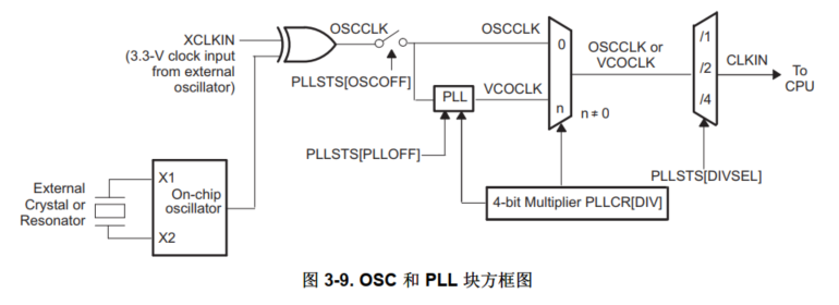 As can be seen from the figure, the chip clock is as follows: for the external crystal oscillator input, PLLSTS (OSCOFF) selects whether to input, and then selects OSCCLK or from PLL. If PLL input, it is enabled by PLLSTS(PLLOFF), PLLCR (DIV), frequency doubling and PLLSTS (DIVSEL)
InitPll(DSP28_PLLCR,DSP28_DIVSEL);
Set frequency multiplication coefficient and frequency division coefficient
if (SysCtrlRegs.PLLSTS.bit.DIVSEL != 0)
 {
   EALLOW;
   SysCtrlRegs.PLLSTS.bit.DIVSEL = 0;
   EDIS;
 }
Before writing PLLCR, PLLSTS (DIVSEL) must be 0, and it should be changed only when PLLSTS[PLLOCKS]=1.
A frequency divider on the PLL output is necessary to ensure the correct duty cycle of the clock fed into the core. For this reason, the DIVSEL value must not be 3 when PLL is active.
 PLL mode is generally used, with non-zero value N=10, DIVSEL=2, CLKIN=30M*10/2=150M
1.1.2 setting peripheral clock
   SysCtrlRegs.HISPCP.all = 0x0001;
   SysCtrlRegs.LOSPCP.all = 0x0002;

 High speed clock: 75M
Low speed clock: 32.5M
   XintfRegs.XINTCNF2.bit.XTIMCLK = 1;
   XintfRegs.XINTCNF2.bit.CLKMODE = 1;
   XintfRegs.XINTCNF2.bit.CLKOFF = 0;
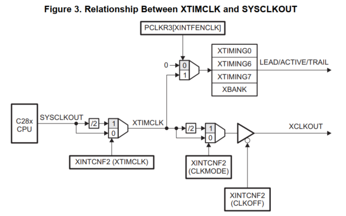 XTIMCLK=75M
XCLKOUT=32.5M
   SysCtrlRegs.PCLKCR0.bit.SPIAENCLK  = 1;   // SPI-A
   SysCtrlRegs.PCLKCR3.bit.DMAENCLK = 1;       // DMA Clock
   SysCtrlRegs.PCLKCR3.bit.XINTFENCLK = 1;     // XTIMCLK
   SysCtrlRegs.PCLKCR3.bit.GPIOINENCLK = 1;    // GPIO input clock
   SysCtrlRegs.PCLKCR0.bit.TBCLKSYNC = 0;   // Disable TBCLK within the ePWM
   SysCtrlRegs.PCLKCR1.bit.EPWM1ENCLK = 1;  // ePWM1
   SysCtrlRegs.PCLKCR1.bit.EPWM2ENCLK = 1;  // ePWM2
   SysCtrlRegs.PCLKCR1.bit.EPWM3ENCLK = 1;  // ePWM3
   SysCtrlRegs.PCLKCR1.bit.EPWM4ENCLK = 1;  // ePWM4
   SysCtrlRegs.PCLKCR1.bit.EPWM5ENCLK = 1;  // ePWM5
   SysCtrlRegs.PCLKCR1.bit.EPWM6ENCLK = 1;  // ePWM6
   SysCtrlRegs.PCLKCR0.bit.TBCLKSYNC = 1;   // Enable TBCLK within the ePWM
Turn on SPIA, EPWM, DMA, GPIO and XTIMCLK clocks
 SPIA's clock is LSPCLK=32.5M
1.2 initialize GPIO of external interface
void InitXintf16Gpio()
{
     EALLOW;
     GpioCtrlRegs.GPCMUX1.bit.GPIO64 = 3;  // XD15
     GpioCtrlRegs.GPCMUX1.bit.GPIO65 = 3;  // XD14
     GpioCtrlRegs.GPCMUX1.bit.GPIO66 = 3;  // XD13
     GpioCtrlRegs.GPCMUX1.bit.GPIO67 = 3;  // XD12
     GpioCtrlRegs.GPCMUX1.bit.GPIO68 = 3;  // XD11
     GpioCtrlRegs.GPCMUX1.bit.GPIO69 = 3;  // XD10
     GpioCtrlRegs.GPCMUX1.bit.GPIO70 = 3;  // XD19
     GpioCtrlRegs.GPCMUX1.bit.GPIO71 = 3;  // XD8
     GpioCtrlRegs.GPCMUX1.bit.GPIO72 = 3;  // XD7
     GpioCtrlRegs.GPCMUX1.bit.GPIO73 = 3;  // XD6
     GpioCtrlRegs.GPCMUX1.bit.GPIO74 = 3;  // XD5
     GpioCtrlRegs.GPCMUX1.bit.GPIO75 = 3;  // XD4
     GpioCtrlRegs.GPCMUX1.bit.GPIO76 = 3;  // XD3
     GpioCtrlRegs.GPCMUX1.bit.GPIO77 = 3;  // XD2
     GpioCtrlRegs.GPCMUX1.bit.GPIO78 = 3;  // XD1
     GpioCtrlRegs.GPCMUX1.bit.GPIO79 = 3;  // XD0

     GpioCtrlRegs.GPBMUX1.bit.GPIO40 = 3;  // XA0/XWE1n
     GpioCtrlRegs.GPBMUX1.bit.GPIO41 = 3;  // XA1
     GpioCtrlRegs.GPBMUX1.bit.GPIO42 = 3;  // XA2
     GpioCtrlRegs.GPBMUX1.bit.GPIO43 = 3;  // XA3
     GpioCtrlRegs.GPBMUX1.bit.GPIO44 = 3;  // XA4
     GpioCtrlRegs.GPBMUX1.bit.GPIO45 = 3;  // XA5
     GpioCtrlRegs.GPBMUX1.bit.GPIO46 = 3;  // XA6
     GpioCtrlRegs.GPBMUX1.bit.GPIO47 = 3;  // XA7

     //postposed
     GpioCtrlRegs.GPBMUX2.bit.GPIO54 = 3;
     GpioCtrlRegs.GPBMUX2.bit.GPIO55 = 3;
     GpioCtrlRegs.GPBMUX2.bit.GPIO56 = 3;
     GpioCtrlRegs.GPBMUX2.bit.GPIO57 = 3;

     GpioCtrlRegs.GPCMUX2.bit.GPIO80 = 3;  // XA8
     GpioCtrlRegs.GPCMUX2.bit.GPIO81 = 3;  // XA9
     GpioCtrlRegs.GPCMUX2.bit.GPIO82 = 3;  // XA10
     GpioCtrlRegs.GPCMUX2.bit.GPIO83 = 3;  // XA11
     GpioCtrlRegs.GPCMUX2.bit.GPIO84 = 3;  // XA12
     GpioCtrlRegs.GPCMUX2.bit.GPIO85 = 3;  // XA13
     GpioCtrlRegs.GPCMUX2.bit.GPIO86 = 3;  // XA14
     GpioCtrlRegs.GPCMUX2.bit.GPIO87 = 3;  // XA15
     GpioCtrlRegs.GPBMUX1.bit.GPIO39 = 3;  // XA16
     GpioCtrlRegs.GPAMUX2.bit.GPIO31 = 3;  // XA17
     GpioCtrlRegs.GPAMUX2.bit.GPIO30 = 3;  // XA18
     GpioCtrlRegs.GPAMUX2.bit.GPIO29 = 3;  // XA19


     GpioCtrlRegs.GPBMUX1.bit.GPIO34 = 3;  // XREADY
	 GpioCtrlRegs.GPBMUX1.bit.GPIO35 = 3;  // XRNW
     GpioCtrlRegs.GPBMUX1.bit.GPIO38 = 3;  // XWE0

     GpioCtrlRegs.GPBMUX1.bit.GPIO36 = 3;  // XZCS0
     GpioCtrlRegs.GPBMUX1.bit.GPIO37 = 3;  // XZCS7
     GpioCtrlRegs.GPAMUX2.bit.GPIO28 = 3;  // XZCS6

     EDIS;
}
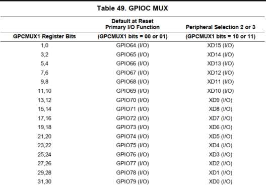 Data cable, XD0-15
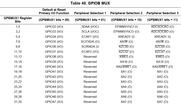
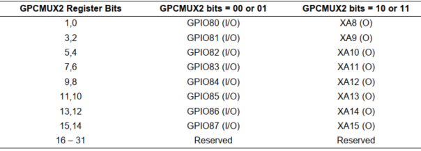
 Address line: XA0-XA19,
Control line: XREADY, XR/W, XWE0, XZCS0, XZCS7, XZCS6
1.4 initialize GPIO of SPIA interface

void InitSpiaGpio()
{

    EALLOW;
    GpioCtrlRegs.GPBPUD.bit.GPIO54 = 0;   // Enable pull-up on GPIO54 (SPISIMOA)
    GpioCtrlRegs.GPBPUD.bit.GPIO55 = 0;   // Enable pull-up on GPIO55 (SPISOMIA)
    GpioCtrlRegs.GPBPUD.bit.GPIO56 = 0;   // Enable pull-up on GPIO56 (SPICLKA)
    GpioCtrlRegs.GPBPUD.bit.GPIO57 = 0;   // Enable pull-up on GPIO57 (SPISTEA)
    GpioCtrlRegs.GPBQSEL2.bit.GPIO54 = 3; // Asynch input GPIO54 (SPISIMOA)
    GpioCtrlRegs.GPBQSEL2.bit.GPIO55 = 3; // Asynch input GPIO55 (SPISOMIA)
    GpioCtrlRegs.GPBQSEL2.bit.GPIO56 = 3; // Asynch input GPIO56 (SPICLKA)
    GpioCtrlRegs.GPBQSEL2.bit.GPIO57 = 3; // Asynch input GPIO57 (SPISTEA)
    GpioCtrlRegs.GPBMUX2.bit.GPIO54 = 1; // Configure GPIO54 as SPISIMOA
    GpioCtrlRegs.GPBMUX2.bit.GPIO55 = 1; // Configure GPIO55 as SPISOMIA
    GpioCtrlRegs.GPBMUX2.bit.GPIO56 = 1; // Configure GPIO56 as SPICLKA
    GpioCtrlRegs.GPBMUX2.bit.GPIO57 = 0; // Configure GPIO57 as SPISTEA
    //GpioCtrlRegs.GPBMUX2.bit.GPIO57 = 1;
   EDIS;
}
Pull up, function selection, sampling interval
1.4.1 GPIO configuration
void gpio_config(void)
{
	EALLOW;
	 GpioCtrlRegs.GPBDIR.bit.GPIO57 = 1;//output
	 GpioCtrlRegs.GPBDIR.bit.GPIO56 = 0;//input
	 GpioCtrlRegs.GPAMUX1.bit.GPIO0 = 0;//Ordinary io
	 GpioCtrlRegs.GPADIR.bit.GPIO0 = 1;//output

	 EDIS;
}
The clock is the input. Chip selection is output and GPIO0 is normal IO
1.5 interrupt initialization
DINT;
InitPieCtrl();
IER = 0x0000;
IFR = 0x0000;
InitPieVectTable();
1.6 SPI initialization
void spi_init()
{
	SpiaRegs.SPICCR.bit.SPISWRESET = 0;//
	SpiaRegs.SPICCR.all = 0x0047;		//The SPI software resets the polarity bit
											//to 1 (sending data along the falling edge),
											//moving in and out of the 8 bit word length each time,
											//and prohibiting the SPI internal loopback (LOOKBACK) function;

	SpiaRegs.SPICTL.all = 0x0006;		// 0111 Enable master mode, normal phase, // enable talk, and SPI int disabled.
	SpiaRegs.SPISTS.all = 0x0000;		//Overflow interrupt, prohibit SPI interrupt;
	SpiaRegs.SPIBRR = 0x001F;			//SPI baud rate = 37.5M/24=1.5MHZ;
	SpiaRegs.SPIPRI.bit.FREE = 1;		//Set so breakpoints don't disturb xmission
	SpiaRegs.SPIFFTX.bit.SPIFFENA = 0;
	SpiaRegs.SPICCR.bit.SPISWRESET = 1;
}


First set the SPICCR register's spicwreset to zero, then operate, and then set to 1
SPICCR=0x0047 =1000 0111
SPISWRESET=1; Reset failure
CLOCK POLARITY=0; Rising edge output, falling edge receive. It works together with CLOCK PHASE to form four SPI working modes
SPILBK=0; Loopback mode off
The lower four bits are byte length selection bits: 0111, which represents the byte length of 8 bits
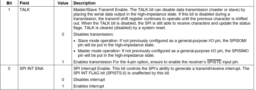
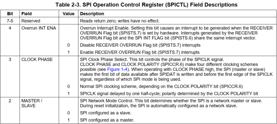
SPICTL=0x0006=0000 0110
Bit 0: turn off interrupt enable
Bit 1: enable 4-pin transmission
Bit 2: host mode
Bit 3: no clock delay
Bit 4: shutdown interrupt
SpiaRegs.SPISTS.all = 0x0000; Write zero
SPIBRR=0x001f=32.5/25=1.3MHz baud rate

SpiaRegs.SPIPRI.bit.FREE = 1; SPI keeps running spiaregs SPIFFTX. bit. SPIFFENA = 0; Close FIFO
Reset W5500.7
void Reset_W5500(void)
{
	GpioDataRegs.GPADAT.bit.GPIO0 = 0;
	delay_loop();
	GpioDataRegs.GPADAT.bit.GPIO0 = 1;
	delay_loop();
}
1.8 set default MAC, IP, GW, SUB and DNS
uint8 mac[6]={0x00,0x08,0xdc,0x11,0x11,0x12};
  uint8 lip[4]={192,168,1,150};
  uint8 sub[4]={255,255,255,0};
  uint8 gw[4]={192,168,1,1};
  uint8 dns[4]={8,8,8,8};
  memcpy(ConfigMsg.lip, lip, 4);
  //printf("lip: %d.%d.%d.%d\r\n",lip[0],lip[1],lip[2],lip[3]);
  memcpy(ConfigMsg.sub, sub, 4);
 // printf("sub: %d.%d.%d.%d\r\n",sub[0],sub[1],sub[2],sub[3]);
  memcpy(ConfigMsg.gw,  gw, 4);
  //printf("gw: %d.%d.%d.%d\r\n",gw[0],gw[1],gw[2],gw[3]);
  memcpy(ConfigMsg.mac, mac,6);

  memcpy(ConfigMsg.dns,dns,4);
  //printf("dns: %d.%d.%d.%d\r\n",dns[0],dns[1],dns[2],dns[3]);
1.9 set the network, that is, set the register of W5500
void set_network(void)			// Configure and print IP information, and initialize 8 sockets
{
  uint8 ip[4];
  setSHAR(ConfigMsg.mac);
  //printf("mac:");
  setSUBR(ConfigMsg.sub);
  setGAR(ConfigMsg.gw);
  setSIPR(ConfigMsg.lip);

  sysinit(txsize, rxsize); 											// Initialize 8 socket s
  setRTR(2000);														// Set timeout
  setRCR(3);														// Set maximum number of resends

  getSIPR (ip);
  printf("IP : %d.%d.%d.%d\r\n", ip[0],ip[1],ip[2],ip[3]);
  getSUBR(ip);
  printf("SN : %d.%d.%d.%d\r\n", ip[0],ip[1],ip[2],ip[3]);
  getGAR(ip);
  printf("GW : %d.%d.%d.%d\r\n", ip[0],ip[1],ip[2],ip[3]);
}
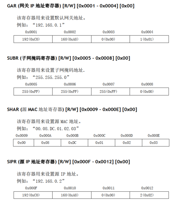 After this step, the W5500 and the upper computer can be connected
Initialization Socket size: 8, each 2k
Setting the timeout time and the maximum number of times of sending are both register settings
1.10 while(1) function, switch statement
Read the four states of W5500, which are SOCK_CLOSED,SOCK_INIT,SOCK_ESTABLISHED,SOCK_CLOSE_WAIT
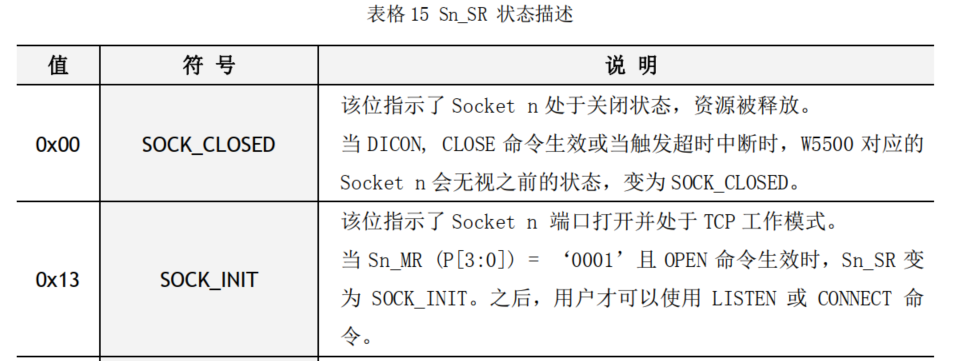
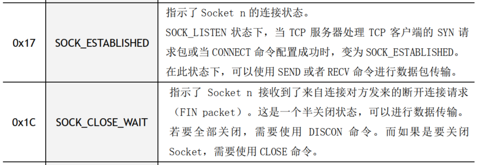 The first state read is SOCK_CLOSED
Then set the mode to TCP/IP mode
socket(0,Sn_MR_TCP,local_port,Sn_MR_ND);
Mainly for Sn_MR register operation
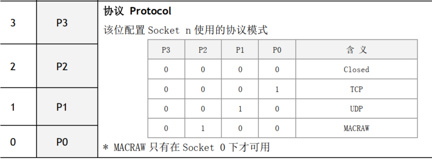 The 0-3 bits are set to 0001
 The fifth bit is set to 1 without delay.
 IINCHIP_WRITE(Sn_PORT0(s) ,(uint8)((local_port & 0xff00) >> 8));
 IINCHIP_WRITE(Sn_PORT1(s) ,(uint8)(local_port & 0x00ff));
Port settings for channel 0
IINCHIP_WRITE( Sn_CR(s) ,Sn_CR_OPEN); // run sockinit Sn_CR
Write OPEN command
At this time:
 Sn_SR becomes 0x13, which is SOCK_INT
case SOCK_INIT://Step 2: initialize and connect to the server
connect(0, server_ip,server_port);
	break;
After initializing the state, use the connect command
It refers to the ip and port connected to the server, indicating that the channel is used as the client mode
If it is listening, it is server mode
 After the connection command is successful, SN_SR will change to 0x17, which is sock_ In the established state, you can use the send and receive commands
1.11 program after selecting establish
if(getSn_IR(0) & Sn_IR_CON)
{
	setSn_IR(0, Sn_IR_CON);
}
Read SN_ The value of IR to judge whether it is Sn_IR_CON,
Then Sn_IR_CON write Sn_IR
In essence, it is a problem of interrupt clearing
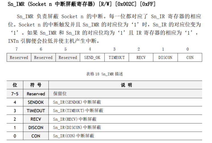
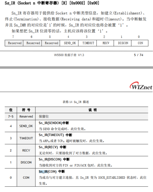 After clearing, read SN_ RX_ Value of RSR register, idle receive cache register
len=getSn_RX_RSR(0);//Read byte size of receive cache
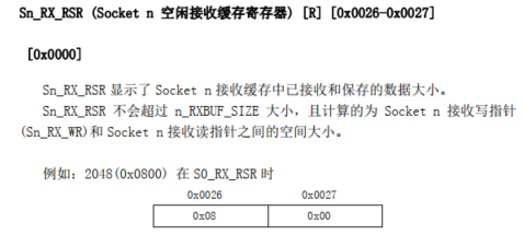 If there is data
First clear the buffer and buffer16 arrays, one is 8 bits and the other is 16 bits
recv(0,buffer,len);//Write data of W5500 to array buffer
Use the recv command to write the data received by the W5500 from the upper computer into the buffer array
8-bit data
for(i=0,j=0;j<1024;i++,j++)//Convert the eight bit data of buffer into 16 bit data of buffer array
{
	temp1=buffer[i];
    temp1=(temp1<<8);
    temp1=temp1&0xff00;
    temp2=buffer[i+1];
    i++;
  	temp2=temp2&0x00ff;
  	buffer16[j]=temp1|temp2;
}
Store the 8-bit data in the buffer into buffer 16, and convert the 8-bit data into 16 bit data
1.12 data related to FPGA operation
The above is a processing process. From here, give the data practical significance
The data transmitted from the upper computer will have a header, indicating the beginning of the data
for(i=0;i<1024;i++)		//Check the beginning of the data. I think it's better to use the while function, but count
  	{
  	  	if(buffer16[i]==0xaa)
  	  		{
  	  			tempstart=i+1;
  	  			break;
  	  		}
  	}
Write the next seven 16 bit data into the cmddata [] array
delaytime=cmddata[1]*100;		//cmddata[1] represents delay time
downdata=(uint16 *)0xC000;

for(i=0;i<cmddata[6];i++)		//cmddata[6] represents the command of how many words are left behind
{
*downdata=buffer16[tempstart];	//Write cmddata[6] data from 0xC000 to 0x8000+cmddata[6]
downdata++;
tempstart++;
}
So far, all commands have reached the corresponding positions:
0xaa cmddata[0]...cmddata[6] downdata[0]...downdata[cmddata[6]-1]
A total of cmddata[6]+8 16 bit data constitute a downhole instrument command
Reset the pointer of downdata
So far, we have started to operate the FPGA. Each operation will have practical significance in the FPGA, which needs to be seen together with the FPGA part
downdata=(uint16 *)0xC000;//Pointer reset

*wrctrl=0x1f1;		//To set the register wrctrl, you need to see the fpga program
status_edib=*rdstatus;			//Read register rdstatus
while(checkbit16(status_edib,0)==1)			//When the last digit is 1
{
     status_edib=*rdstatus;
}
*wrcmd=cmddata[0];		//Write data of cmddata[0] to wrcmd address
Write 1 111 0001 to the write control register wrctrl
Read the value of rdstatus and proceed to the next step when bit 0 is not 1
Write data of cmddata[0] to wrcmd
for(i=0;i<cmddata[6];i++)//When the last bit of rdstatus is 1 every time, write the data of downdata to wrdata
    {
        status_edib=*rdstatus;
        while(checkbit16(status_edib,0)==1)
        {
          status_edib=*rdstatus;
        }
       temp=*downdata;
       *wrdata=temp;
       downdata++;
    }
stay rdstatus When the last digit is not 1, the downdata Data writing for wrdata
 for(z=0;z<delaytime;z++)
  	{
  	  	for(j=0;j<35;j++)
  	  		 {
  	  			asm(" nop ");
  	  		}
  	  	 asm(" nop ");
  	}
if(cmddata[2]!=0)	//The use of cmddata [0] and [2] depends on the meaning of wrcmd
  	 {
  	  		status_edib=*rdstatus;
  	  		while(checkbit16(status_edib,0)==1)
  	  			 {
  	  				 status_edib=*rdstatus;
  	  			}
  	  		 *wrcmd=cmddata[2];
  	  			 }
After the delay, write the data of cmddata[2] to wrcmd
   /******** wait for encode  *******/
       status_edib=*rdstatus;											//When rdstatus = xxx0x, the decoding is completed
  while((checkbit16(status_edib,1)==0))
  {
      status_edib=*rdstatus;
 }
    status_edib=*rdstatus;
    while((checkbit16(status_edib,2)!=0))
    {
        status_edib=*rdstatus;
    }
    status_edib=*rdstatus;
/****************************************
When / / rdstatus = xxxx10x, the decoding is completed
Write 1 1111 1010 to wrctrl
Define where the data will be stored
Write the data of the three channels to the address of the defined extended ram in turn
*wrctrl=0x1fc;																		//wrctrl is a very important register, which needs to be understood from fpga
extram=(Uint32 *)0x200000;
extram2=(Uint32 *)0x200000;
extram5=(Uint32 *)(0x200000+cmddata[3]*2);
extram7=(Uint32 *)(0x200000+cmddata[3]*2+cmddata[4]*2);
timeout_num=0;
while((m2<cmddata[3]||m5<cmddata[4]||m7<cmddata[5])&&(timeout_num<2000))
{
   status_edib=*rdstatus;
   if(checkbit16(status_edib,1)==0)
   {
     temp=*rdm2fifo;
     *extram2=temp;
     m2++;
     *extram2++;
     timeout_num=0;
   }
   if(checkbit16(status_edib,5)==0)
   {
     temp=*rdm5fifo;
     *extram5=temp;
     m5++;
     *extram5++;
     timeout_num=0;
   }
   if(checkbit16(status_edib,7)==0)
   {
      temp=*rdm7fifo;
      *extram7=temp;
      m7++;
      *extram7++;
      timeout_num=0;
   }
   if((checkbit16(status_edib,1)!=0)&&(checkbit16(status_edib,5)!=0)&&(checkbit16(status_edib,7)!=0))
   {
      for(i=0;i<30;i++)
      {
         asm(" nop ");
      }
      timeout_num++;
   }
}
//The data has reached 0x200000
num=m2+m5+m7;
Then read the data from the external expansion ram, divide the 16 bit data into 8 data and write them into the buffer, and transmit every 2048 8 8-bit data
   for(i=0,j=0;i<num;i++)
      {
         temp32=*extram;
         temp32=(Uint16)temp32;
         temp321=temp32>>8;
         temp322=temp32&0xff;
         buffer[j]=temp321;
         j++;
         buffer[j]=temp322;
         j++;
         *extram++;
         if(j==2048)
         {
        	send(0,buffer,2048);
        	j=0;
        	memset(buffer,0,sizeof(buffer));
         }
      }
	send(0,buffer,2048);
	}
So far, the content of DSP is completed, and then the CMD file and the stored mapping are described
1.13 CMD file and storage mapping
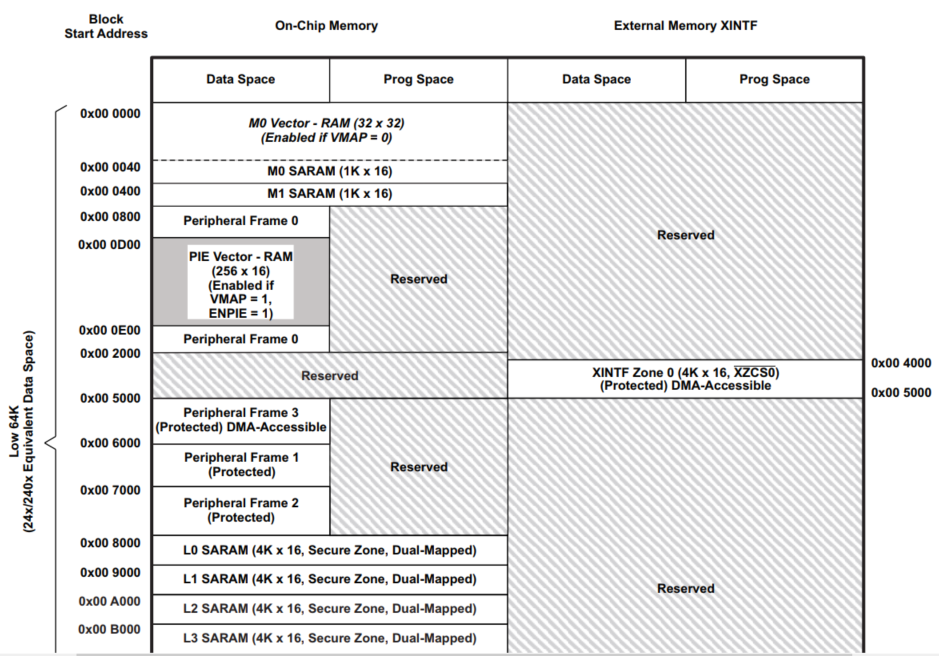
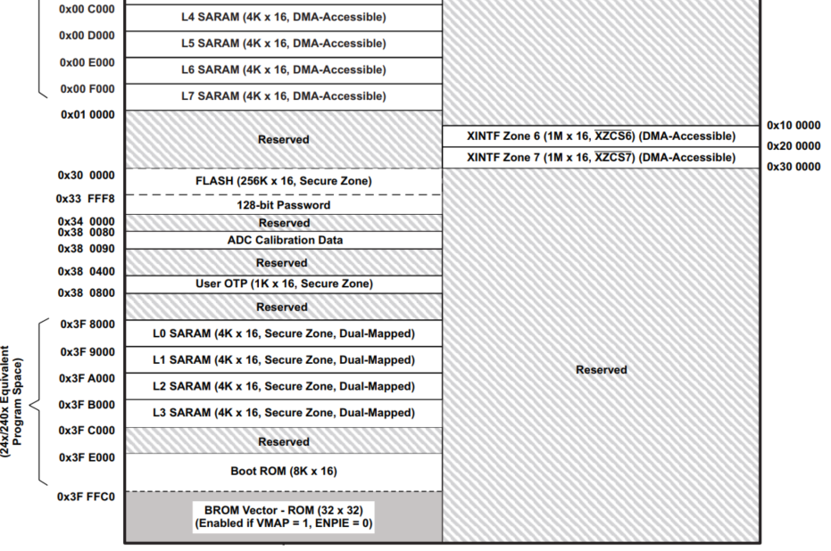 In fact, there are only three areas that need to be set by ourselves, and the others are consistent with the original document
1: The data storage area issued is the command for downhole instruments, which is mainly stored in 0xC000~0xF000
This is in the film
RAML : origin = 0x008000, length = 0x004000
2: For the area of FPGA expansion, the expansion partition xinf zone0 0x4000-0x5000 is selected, and the chip selection signal line is XZCS0
`ZONE0: origin = 0x004000, length = 0x001000 /* XINTF zone 0 - data space`
3: The external expansion area of SRAM is xinf zone7 0x200000 ~ 0x300000 The chip selection signal line is XZCS7
ZONE7B : origin = 0x200000, length = 0x010000 /* XINTF zone 7 - data space */
1.14 effective time of signal line and address line (effective period)
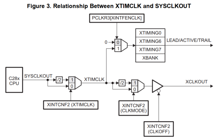 It is known from the analysis in 1.1.2 that XTIMCLK=75M
As analyzed above, the main storage area uses three areas. Now it mainly describes two areas outside the chip
Xintf Zone0, area: 0x004000-0x005000
In xintf Configuration in C
First, configure all partitions:


XintfRegs.XINTCNF2.bit.XTIMCLK = 1;
// No write buffering
XintfRegs.XINTCNF2.bit.WRBUFF = 0;
// XCLKOUT is enabled
XintfRegs.XINTCNF2.bit.CLKOFF = 0;
// XCLKOUT = XTIMCLK/2
XintfRegs.XINTCNF2.bit.CLKMODE = 0;
As shown in the figure above, xtimclk = 75m, xclkout = 32.5m
1.14.1 next, configure Zone 0
   // Zone 0------------------------------------
    // When using ready, ACTIVE must be 1 or greater
    // Lead must always be 1 or greater
    // Zone write timing
    XintfRegs.XTIMING0.bit.XWRLEAD = 3;
    XintfRegs.XTIMING0.bit.XWRACTIVE = 3;
    XintfRegs.XTIMING0.bit.XWRTRAIL = 3;
    // Zone read timing
    XintfRegs.XTIMING0.bit.XRDLEAD = 3;
    XintfRegs.XTIMING0.bit.XRDACTIVE = 3;
    XintfRegs.XTIMING0.bit.XRDTRAIL = 3;
    // double all Zone read/write lead/active/trail timing
    XintfRegs.XTIMING0.bit.X2TIMING = 1;
    // Zone will sample XREADY signal
    XintfRegs.XTIMING0.bit.USEREADY = 0;
    // Size must be either:
    // 0,1 = x32 or
    // 1,1 = x16 other values are reserved
    XintfRegs.XTIMING0.bit.XSIZE = 3;


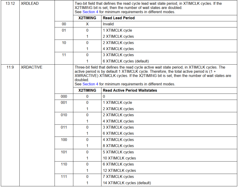
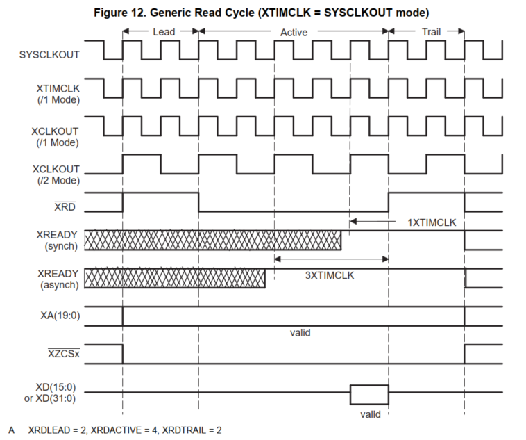
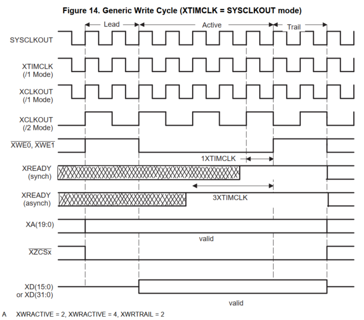
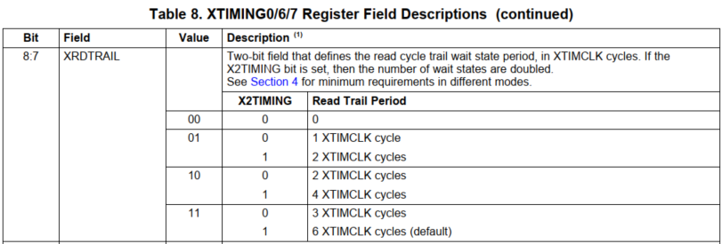 16 bit data length without READY signal. The length of LEAD, ACTIVE and TRAIL is 6 XTIMCLK cycles, that is, 6 75M cycles = 12.5M, that is, 6/75M seconds
The cycle of reading and writing is the same. Because the partition operates on FPGA, the cycle is relatively long
1.14.2 next, configure Zone 7
Zone 7 is the signal of expanded RAM
// Zone 7------------------------------------
// When using ready, ACTIVE must be 1 or greater
// Lead must always be 1 or greater
// Zone write timing
XintfRegs.XTIMING7.bit.XWRLEAD = 1;
XintfRegs.XTIMING7.bit.XWRACTIVE = 1;
XintfRegs.XTIMING7.bit.XWRTRAIL = 1;
// Zone read timing
XintfRegs.XTIMING7.bit.XRDLEAD = 1;
XintfRegs.XTIMING7.bit.XRDACTIVE = 1;
XintfRegs.XTIMING7.bit.XRDTRAIL = 1;

// double all Zone read/write lead/active/trail timing
XintfRegs.XTIMING7.bit.X2TIMING = 0;

// Zone will sample XREADY signal
XintfRegs.XTIMING7.bit.USEREADY = 0;


// Size must be either:
// 0,1 = x32 or
// 1,1 = x16 other values are reserved
XintfRegs.XTIMING7.bit.XSIZE = 3;
Not mentioned above. Its cycle is one XTIMCLK cycle
1.14.3 BANK signal
XintfRegs.XBANK.bit.BANK = 4;
XintfRegs.XBANK.bit.BCYC = 0;
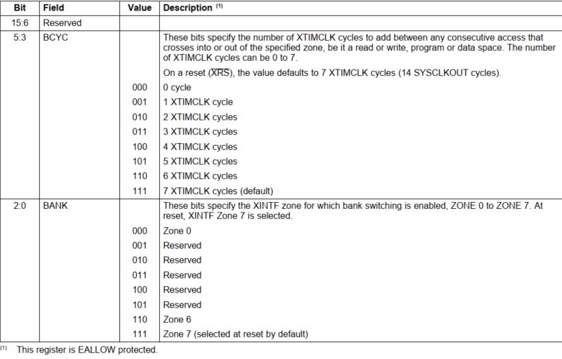 Zone 0 is relatively slow, so BANK selects zone 0 and gives it 4 cycles to buffer
For specific functions, refer to the documentation of xinf of 28335
The following is the reference timing of reading and writing of data bus and address bus
