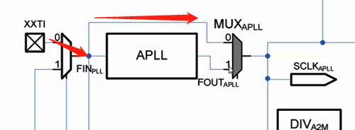
①. First, choose not to use PLL. Let the external 24MHz raw clock pass directly and bypass the APLL path
.global clock_init
clock_init:
	ldr	r0, =ELFIN_CLOCK_POWER_BASE

	// 1 set various clock switches and do not use PLL for the time being
	ldr	r1, =0x0
	// Chip manual P378 register CLK_SRC: Select clock source 0 (Main)
	str	r1, [r0, #CLK_SRC0_OFFSET]
ldr r0, =ELFIN_CLOCK_POWER_BASE # All register addresses are in elf_ CLOCK_ POWER_ Base accumulation is OK. Here is the address of the basic register
// 1 set various clock switches and do not use PLL for the time being
ldr r1, =0x0
// Chip manual P378 register CLK_SRC: Select clock source 0 (Main)
str r1, [r0, #CLK_SRC0_OFFSET]
#In ELF_ CLOCK_ POWER_ BASE On the basis of CLK_SRC0_OFFSET gets r1 address
# r0 It's CLK_SRC0 has 32 Positions in total. Set all bits to 0
** CLK_SRC0 register is to set the MUX switch. For example, set all the modified registers to 0, and the main bit0 and bit4 to 0, indicating that APLL and MPLL registers EPLL are not turned on temporarily
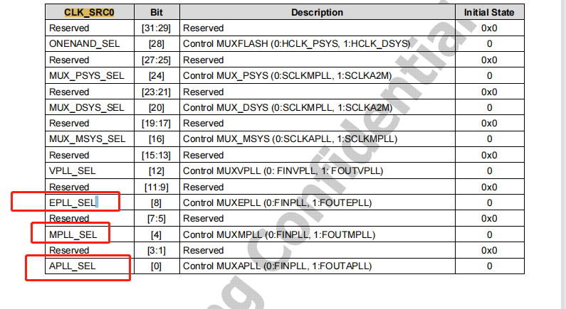
Here is APLL_SEL 0 It's FINPLL. Take the following route. It doesn't go through frequency doubling when powered on. The default is 24M
If APLL_SEL 1 is output through APLL FOUT
②. Set the lock time after iROM initializes the system clock.
	// 2. Set the locking time and use the default value
	// After setting the PLL, it takes a certain time to raise the clock from Fin to the target frequency, that is, the locking time
	ldr	r1,	=0x0000FFFF
	str	r1,	[r0, #APLL_LOCK_OFFSET]
	str r1, [r0, #MPLL_LOCK_OFFSET]
At the beginning, there was no APLL, but later, there was APLL, Set the lock time. As soon as APLL is turned on, the clock will not come right away, After the delay, let the clock come. The default time is 0xFFF, now the maximum is 0xFFFF
Schematic description: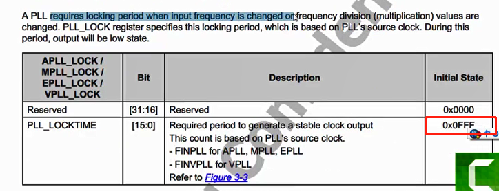
③. Set the frequency division system to determine how to divide the highest clock from PLL to obtain each sub clock
	// 3 set frequency division
	// Clear bit[0~31]
	ldr r1, [r0, #CLK_DIV0_OFFSET]
	ldr	r2, =CLK_DIV0_MASK
	bic	r1, r1, r2
	ldr	r2, =0x14131440
	orr	r1, r1, r2
	str	r1, [r0, #CLK_DIV0_OFFSET]
ldr r1, [r0, #CLK_DIV0_OFFSET] namely CLK_ Div0 register Set to 0x14131440 0x14131440 namely 00010100000100110001010001000000
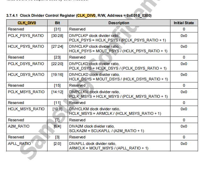
0001 [30:28]: PCLK_PSYS_RATIO =1
HCLK_PSYS = MOUT_PSYS / (4 + 1)
PCLK_DSYS = HCLK_DSYS / (1+ 1)
........
HCLK_MSYS = ARMCLK / (4+ 1)
ARMCLK = MOUT_MSYS / (0 + 1)
④. Setting PLL mainly sets the frequency doubling system of PLL to determine how much output frequency can be obtained from the original frequency of 24MHz at the input end. After setting, the output ARMCLK is 1GHz Set CON
	// 4 set PLL
	// FOUT = MDIV*FIN/(PDIV*2^(SDIV-1))=0x7d*24/(0x3*2^(1-1))=1000 MHz
	ldr	r1, =APLL_VAL
	str	r1, [r0, #APLL_CON0_OFFSET]
	// FOUT = MDIV*FIN/(PDIV*2^SDIV)=0x29b*24/(0xc*2^1)= 667 MHz
	ldr	r1, =MPLL_VAL
	str	r1, [r0, #MPLL_CON_OFFSET]
FOUT = MDIV*FIN/(PDIV*2^(SDIV-1))=0x7d*24/(0x3*2^(1-1))=1000 MHz
FOUT is 1G and FIN is 24 0x7d 0x3 these are from Samsung
#define set_pll(mdiv, pdiv, sdiv) (1<<31 | mdiv<<16 | pdiv<<8 | sdiv)
#define APLL_VAL set_pll(APLL_MDIV,APLL_PDIV,APLL_SDIV) Put MPS into APLL_VAL

//These M, P and S configuration values are obtained by referring to the recommended configuration of typical clock configuration values in the data manual.
//These configuration values are recommended by Samsung, so they work most stably. If it's made up by yourself, you should
//After strict testing, we can ensure that it is right.
// Put these values in APLL_ In the con0 register, these need M, P, S settings, all of which can be found in the manual

⑤. Open PLL. All switches and frequency division coefficients have been set in the previous four steps. In this step, after opening the PLL, the PLL starts to work, locks the frequency and outputs it, and then obtains each frequency through frequency division
	// 5 set various clock switches and use PLL
	ldr	r1, [r0, #CLK_SRC0_OFFSET]
	ldr	r2, =0x10001111
	orr	r1, r1, r2
	str	r1, [r0, #CLK_SRC0_OFFSET]

	mov	pc, lr
CLK_SRC0 ,
00010000000000000001000100010001
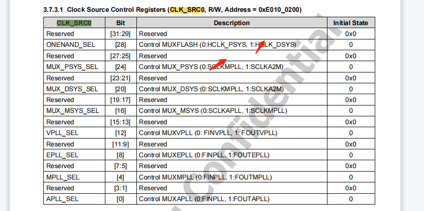
MUXFLASH = 1
MUX_PSYS =0
Control MUX_DSYS = 0

APLL comes out 1000, ARMCLK = 1000 HCLK_MSYS = 1000/5 = 200 ....
MPLL = 667 ,

Finally, the typical value is calculated:
Full code:
// Clock controller base address
#define ELFIN_CLOCK_POWER_BASE		0xE0100000

// The offset value of the clock related register from the base address of the clock controller
#define APLL_LOCK_OFFSET		0x00
#define MPLL_LOCK_OFFSET		0x08

#define APLL_CON0_OFFSET		0x100
#define APLL_CON1_OFFSET		0x104
#define MPLL_CON_OFFSET			0x108

#define CLK_SRC0_OFFSET			0x200
#define CLK_SRC1_OFFSET			0x204
#define CLK_SRC2_OFFSET			0x208
#define CLK_SRC3_OFFSET			0x20c
#define CLK_SRC4_OFFSET			0x210
#define CLK_SRC5_OFFSET			0x214
#define CLK_SRC6_OFFSET			0x218
#define CLK_SRC_MASK0_OFFSET	0x280
#define CLK_SRC_MASK1_OFFSET	0x284

#define CLK_DIV0_OFFSET			0x300
#define CLK_DIV1_OFFSET			0x304
#define CLK_DIV2_OFFSET			0x308
#define CLK_DIV3_OFFSET			0x30c
#define CLK_DIV4_OFFSET			0x310
#define CLK_DIV5_OFFSET			0x314
#define CLK_DIV6_OFFSET			0x318
#define CLK_DIV7_OFFSET			0x31c

#define CLK_DIV0_MASK			0x7fffffff

// These M, P and S configuration values are obtained by referring to the recommended configuration of typical clock configuration values in the data manual.
// These configuration values are recommended by Samsung, so they work most stably. If it's made up by yourself, you should
// After strict testing, we can ensure that it is right.
#define APLL_MDIV      	 		0x7d		// 125
#define APLL_PDIV       		0x3
#define APLL_SDIV       		0x1

#define MPLL_MDIV				0x29b		// 667
#define MPLL_PDIV				0xc
#define MPLL_SDIV				0x1

#define set_pll(mdiv, pdiv, sdiv)	(1<<31 | mdiv<<16 | pdiv<<8 | sdiv)
#define APLL_VAL			set_pll(APLL_MDIV,APLL_PDIV,APLL_SDIV)
#define MPLL_VAL			set_pll(MPLL_MDIV,MPLL_PDIV,MPLL_SDIV)


.global clock_init
clock_init:
	ldr	r0, =ELFIN_CLOCK_POWER_BASE

	// 1 set various clock switches and do not use PLL for the time being
	ldr	r1, =0x0
	// Chip manual P378 register CLK_SRC: Select clock source 0 (Main)
	str	r1, [r0, #CLK_SRC0_OFFSET]

	// 2. Set the locking time and use the default value
	// After setting the PLL, it takes a certain time to raise the clock from Fin to the target frequency, that is, the locking time
	ldr	r1,	=0x0000FFFF
	str	r1,	[r0, #APLL_LOCK_OFFSET]
	str r1, [r0, #MPLL_LOCK_OFFSET]

	// 3 set frequency division
	// Clear bit[0~31]
	ldr r1, [r0, #CLK_DIV0_OFFSET]
	ldr	r2, =CLK_DIV0_MASK
	bic	r1, r1, r2
	ldr	r2, =0x14131440
	orr	r1, r1, r2
	str	r1, [r0, #CLK_DIV0_OFFSET]

	// 4 set PLL
	// FOUT = MDIV*FIN/(PDIV*2^(SDIV-1))=0x7d*24/(0x3*2^(1-1))=1000 MHz
	ldr	r1, =APLL_VAL
	str	r1, [r0, #APLL_CON0_OFFSET]
	// FOUT = MDIV*FIN/(PDIV*2^SDIV)=0x29b*24/(0xc*2^1)= 667 MHz
	ldr	r1, =MPLL_VAL
	str	r1, [r0, #MPLL_CON_OFFSET]

	// 5 set various clock switches and use PLL
	ldr	r1, [r0, #CLK_SRC0_OFFSET]
	ldr	r2, =0x10001111
	orr	r1, r1, r2
	str	r1, [r0, #CLK_SRC0_OFFSET]

	mov	pc, lr