preface
Jiudao is working on a switching power supply project recently. It needs TI's TMS320F28035 chip to realize the design of control circuit. In short, 28035 is used to collect the semaphore, calculate the algorithm, obtain the duty cycle, and then use the ePWM module to output PWM wave to control the on and off of the power switch, so as to realize the power transformation of the topology.
In order to realize control, we need to realize ADC sampling, duty cycle calculation, etc. in one switching cycle (PWM cycle). So, how to realize ADC sampling in each switching cycle?
The answer is to use the ePWM module to trigger the ADC module for sampling in each PWM cycle. How to configure it?
This is the topic of this article~
Experimental purpose
Through ePWM module and ADC module, ePWM sends SOC(start of conversion) signal in each PWM cycle and triggers ADC for sampling, so as to deeply understand the working principle and configuration details of the two modules.
Experimental requirements
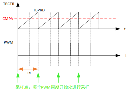
As shown in the figure below, PWM signals with fixed frequency and duty cycle are generated through the ePWM module and sampled at the beginning of each PWM cycle, that is, the sampling frequency is equal to the PWM frequency.
hardware circuit
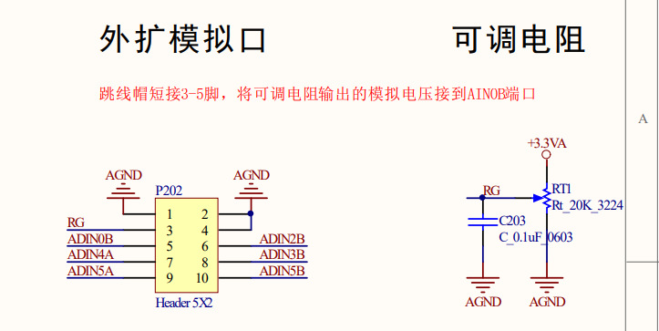
As shown in the figure below, the ADC samples the voltage value of the adjustable resistor through the RG pin and stores it in the result register ADCRESULT. The jumper cap is short circuited to pins 3-5, and the voltage value of the variable resistance is connected to ADIN0B through RG, that is, ADC can sample the variable resistance value through ADIN0B. ADIN0B here refers to GROUP B channel 0 in the 16 channel multiplexed input channel of ADC. See the figure below for details.
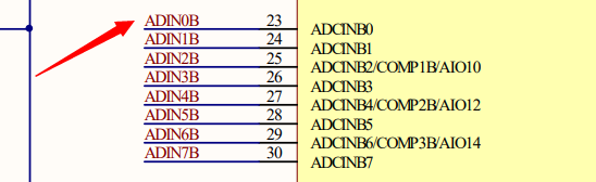
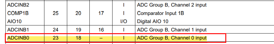
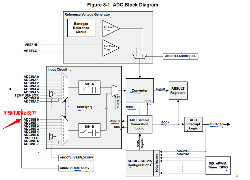
Note that ADCINB0 is an ADC input sampling pin, which is not multiplexed through GPIO. Therefore, GPIO does not need to be configured and can be used directly.
Experimental steps
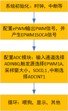
The program flow chart of the whole system is roughly shown in the figure above.
Firstly, some initialization operations of DSP system, including PLL, watchdog, peripheral clock enable, shutdown interrupt, initialization of PIE interrupt vector table, etc.
Secondly, configure the EPWM module to generate PWM with fixed frequency and duty cycle, and set the trigger epwmxsoca (or EPWMxSOCB, select epwmxsoca here) signal.
Then, the ADC module configures the sampling input channel, the trigger source (receiving EPWMxSOCA), the size of the sampling window, and selects a SOCx(x:0-15, here SOC1) for ADC conversion and trigger interrupt ADCINTx(x:1-9).
Finally, enter the loop to feed the dog, display and other background operations. When ADC interrupt occurs, enter the ADC interrupt service function, take out the variable resistance sampling value and save it to the array.
The general process is like this. Of course, the premise of understanding is to fully understand the EPWM module and ADC module of 28035, that is, to be familiar with TI's official user manual and data manual.
In addition, there are many details that have not been mentioned. We mainly refer to the official routines and chip manuals, and then modify them in combination with the requirements.
Code interpretation
#include "DSP28x_Project.h"     // Device Header file and Examples Include File

// Prototype statements for functions found within this file.
__interrupt void adc_isr(void);

// Global variables used in this example:
Uint16 ConversionCount;
Uint16 Voltage1[10];

int main()
{
// Step 1. Initialize System Control:
// PLL, WatchDog, enable Peripheral Clocks
// This example function is found in the DSP2803x_SysCtrl.c file.
   InitSysCtrl();

// Step 2. Initialize GPIO:
// This example function is found in the DSP2803x_Gpio.c file and
// illustrates how to set the GPIO to it's default state.
// InitGpio();  // Skipped for this example

// Step 3. Clear all interrupts and initialize PIE vector table:
// Disable CPU interrupts
   DINT;

// Initialize the PIE control registers to their default state.
// The default state is all PIE interrupts disabled and flags
// are cleared.
// This function is found in the DSP2803x_PieCtrl.c file.
   InitPieCtrl();

// Disable CPU interrupts and clear all CPU interrupt flags:
   IER = 0x0000;
   IFR = 0x0000;

// Initialize the PIE vector table with pointers to the shell Interrupt
// Service Routines (ISR).
// This will populate the entire table, even if the interrupt
// is not used in this example.  This is useful for debug purposes.
// The shell ISR routines are found in DSP2803x_DefaultIsr.c.
// This function is found in DSP2803x_PieVect.c.
   InitPieVectTable();

// Interrupts that are used in this example are re-mapped to
// ISR functions found within this file.
   EALLOW;  // This is needed to write to EALLOW protected register
   PieVectTable.ADCINT1 = &adc_isr;
   EDIS;    // This is needed to disable write to EALLOW protected registers

// Step 4. Initialize all the Device Peripherals:
   InitAdc();  // For this example, initialize the ADC
   AdcOffsetSelfCal();

// Step 5. User specific code, enable interrupts:

// Enable ADCINT1 in PIE
   PieCtrlRegs.PIEIER1.bit.INTx1 = 1;   // Enable INT 1.1 in the PIE for ADCINT1
   IER |= M_INT1;                       // Enable CPU Interrupt 1
   EINT;                                // Enable Global interrupt INTM
   ERTM;                                // Enable Global real time interrupt DBGM

   ConversionCount = 0;

// Configure ADC
// Note: Channel ADCINB0  will be double sampled to workaround the ADC 1st sample issue for rev0 silicon errata

   EALLOW;
   AdcRegs.ADCCTL1.bit.INTPULSEPOS  = 1;    //ADCINT1 trips after AdcResults latch
   AdcRegs.INTSEL1N2.bit.INT1E      = 1;    //Enabled ADCINT1
   AdcRegs.INTSEL1N2.bit.INT1CONT   = 0;    //Disable ADCINT1 Continuous mode
   AdcRegs.INTSEL1N2.bit.INT1SEL    = 1;    //setup EOC1 to trigger ADCINT1 to fire
   AdcRegs.ADCSOC0CTL.bit.CHSEL     = 8;    //set SOC0 channel select to ADCINB0(dummy sample for rev0 errata workaround)
   AdcRegs.ADCSOC1CTL.bit.CHSEL     = 8;    //set SOC1 channel select to ADCINB0
   AdcRegs.ADCSOC0CTL.bit.TRIGSEL   = 5;    //set SOC0 start trigger on EPWM1A, due to round-robin SOC0 converts first then SOC1
   AdcRegs.ADCSOC1CTL.bit.TRIGSEL   = 5;    //set SOC1 start trigger on EPWM1A, due to round-robin SOC0 converts first then SOC1
   AdcRegs.ADCSOC0CTL.bit.ACQPS     = 6;    //set SOC0 S/H Window to 7 ADC Clock Cycles, (6 ACQPS plus 1)
   AdcRegs.ADCSOC1CTL.bit.ACQPS     = 6;    //set SOC1 S/H Window to 7 ADC Clock Cycles, (6 ACQPS plus 1)
   EDIS;

// Assumes ePWM1 clock is already enabled in InitSysCtrl();
   EPwm1Regs.ETSEL.bit.SOCAEN   = 1;        // Enable SOC on A group
   EPwm1Regs.ETSEL.bit.SOCASEL  = 1;        // generate SOCx when TBCTR = ZERO
   EPwm1Regs.ETPS.bit.SOCAPRD   = 1;        // Generate pulse on 1st event
   EPwm1Regs.CMPA.half.CMPA     = 0x0080;   // Set compare A value
   EPwm1Regs.TBPRD              = 0xFFFF;   // Set period for ePWM1
   EPwm1Regs.TBCTL.bit.CTRMODE  = 0;        // count up and start

// Wait for ADC interrupt
   for(;;)
   {
   }
}

__interrupt void  adc_isr(void)
{
  Voltage1[ConversionCount] = AdcResult.ADCRESULT1; //discard ADCRESULT0 as part of the workaround to the 1st sample errata for rev0
  // If 20 conversions have been logged, start over
  if(ConversionCount == 9)
  {
     ConversionCount = 0;
  }
  else
  {
      ConversionCount++;
  }

  AdcRegs.ADCINTFLGCLR.bit.ADCINT1 = 1;     // Clear ADCINT1 flag reinitialize for next SOC
  PieCtrlRegs.PIEACK.all = PIEACK_GROUP1;   // Acknowledge interrupt to PIE

  return;
}
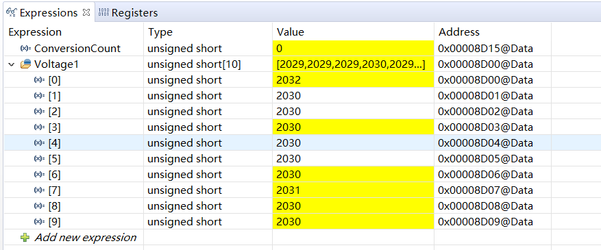
experimental result
After editing the code, burn it into the chip, then Debug, run at full speed, and add sampling values through the window [window - > show view - > expression]. It can be seen that 10 sampling values are refreshed in real time, that is, PWM triggered ADC periodic sampling is realized.
summary
This paper briefly introduces the general design idea and process of generating SOC signal by using EPWM module of TMS320F28035 to trigger ADC module for sampling, and gives the corresponding code and experimental results combined with official routines. The specific configuration process of EPWM module and ADC module related registers is not described in detail. Readers can refer to TI's official Manual:
- 2803x Piccolo Technical Reference Manual.pdf
- tms320f28035.pdf
experience
The author believes that the best way to learn DSP is: official routine + data manual + user manual + development board + CCS.
Specifically, official routines can provide us with a correct overall architecture of the program, such as some initialization steps, which part to initialize first, which part to initialize then, and what to do at last.
The data manual + user manual can be said to be the most important information. You must repeatedly study the original English Version (remember that it is the English version, the Chinese version may have many translation errors, and the author has stepped on the pit), and it is best to study it in combination with the code and take notes for easy review in the future.
After you understand the official routines in conjunction with the data manual and user manual, you can configure yourself. Start a new project at the bottom, write your own code step by step, and then debug it in combination with the CCS + development board.
The time spent debugging the code may be several times more than that spent writing the code, because the program will have many bugs. At this time, check the code line by line in combination with the data manual and user manual, understand the function of each line of code, and think about whether the logic or register configuration is wrong.
When you successfully complete a small experiment from beginning to end and realize the closed loop from theory to experimental verification, I believe your ability and confidence will be improved a lot.