STM32 analog IIC + color recognition TCS34725
1, Hardware parameters
1. Parameters and interfaces
| VCC | 3.3/5V power supply positive |
|---|---|
| GND | Power ground |
| SDA | I2C data input |
| SCL | I2C clock input |
2, Communication protocol
1.IIC sequence diagram
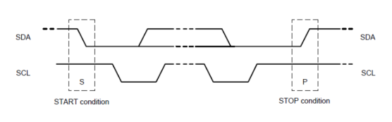
It is known from the I2C sequence diagram that I2C communication, I2C communication, a data line and a clock line are used. I2C bus is transmitting data
There are three types of signals in the process: start signal, end signal and reply signal.
Start signal: when SCL is high level, SDA jumps from high level to low level and starts transmitting data.
End signal: when SCL is high level, SDA jumps from low level to high level and ends data transmission.
Response signal: after receiving 8bit data, the IC receiving the data sends a specific low signal to the IC transmitting the data
Level pulse, indicating that data has been received.
2. Reading and writing sequence
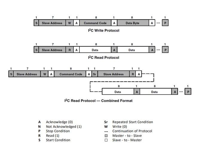
This is a standard IIC communication sequence
1. Write command register timing: start signal - write 7-bit IIC address - write 1-bit read-write identification - wait for slave ack - write command register address - wait for slave ack - write data - wait for slave ACK –... – stop signal.
2. Read command register timing: start signal - write 7-bit IIC address - write 1-bit read-write ID - wait for slave ack - write command register address - wait for slave ack - start signal - write 7-bit IIC address - write 1-bit read-write ID - wait for slave ack - wait for slave data - write reply ack - wait for slave data - write reply ACK –... - stop signal.
Link: https://www.waveshare.net/w/upload/3/3c/TCS34725_Color_Sensro_user_manual_cn.pdf
The user manual of Weixue electronics has detailed instructions, and there are also driver routines.
Three, analog IIC driver
After understanding the communication of IIC, you can write the driver of IIC. I also searched some other simulated IIC communication on the Internet. The programs are similar, basically the same. But after all, some specific details and IO port settings are not very clear. So I won't elaborate on the IIC driver (the program will also be attached below), mainly focusing on some details of my own general section.
1. IO port configuration

Most of the online articles I read basically use push-pull output, and then use the internal register of GPIO (as shown in the figure above) to change the input and output mode of Io. This is indeed feasible, but for Xiaobai who has just learned, it is not very clear to understand the register operation, and this is not applicable to 51 single chip microcomputer. The IO of 51 single chip microcomputer is used as a standard two-way IO port, that is, it can be used as both output and input. Similarly, the open drain output mode is also a two-way IO port, so I personally think it is more convenient and practical to set the IO pin as the open drain output mode.
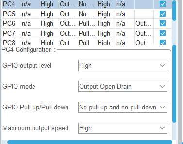
Here I use the PC4 and PCB ports of the single chip microcomputer STMF030RCT6. I use the MXCube to directly configure the open drain floating air. I can also use the code to directly initialize the GPIO port before the program runs.
  GPIO_InitStruct.Pin = GPIO_PIN_4|GPIO_PIN_5;
  GPIO_InitStruct.Mode = GPIO_MODE_OUTPUT_OD;  //Open drain output
  GPIO_InitStruct.Pull = GPIO_NOPULL;		   //Float in the air
  GPIO_InitStruct.Speed = GPIO_SPEED_FREQ_HIGH;
  HAL_GPIO_Init(GPIOC, &GPIO_InitStruct);
GPIO_InitStruct is a structure named GPIO_InitStructure, the structure prototype is composed of GPIO_InitTypeDef determines that it is used to initialize GPIO in STM32.
HAL_ GPIO_ Init (gpioc, & gpio_initstructure). The structure behind the brackets is the one declared in your question. This function is a function encapsulated by Hal library.
2. us delay
IIC delays are microseconds and require accuracy. Generally, STM system delays are milliseconds, which is obviously unusable, so timers have to be used here. I use timer 14 here.
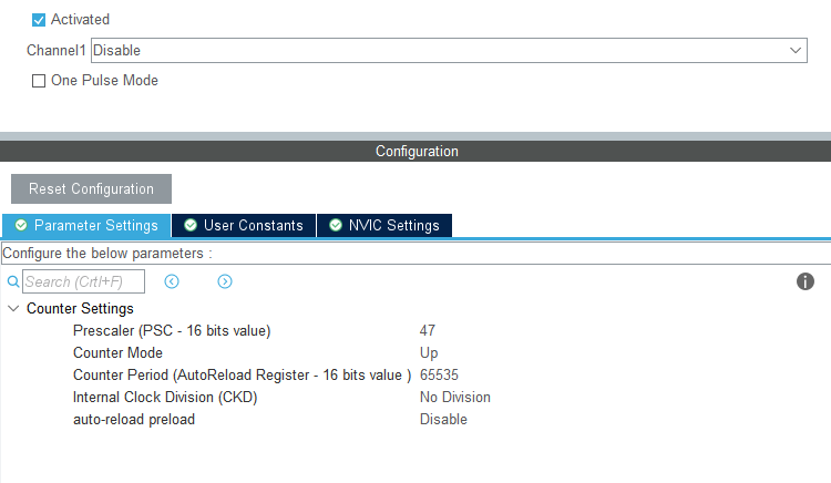
Using the timer, you have to understand the clock frequency of the single chip microcomputer and the pre frequency division coefficient of the timer. The clock frequency of STMF030RCT6 single chip microcomputer is 48MHz. I want to get the timing of 1us, that is, to get the frequency of 1MHz, that is, to divide the frequency 48-1, the pre frequency division coefficient is 47, the automatic reload value is 1, and the upward counting mode.
It can also be implemented in code
static void MX_TIM14_Init(void)
{

  /* USER CODE BEGIN TIM14_Init 0 */

  /* USER CODE END TIM14_Init 0 */

  /* USER CODE BEGIN TIM14_Init 1 */

  /* USER CODE END TIM14_Init 1 */
  htim14.Instance = TIM14;
  htim14.Init.Prescaler = 47;
  htim14.Init.CounterMode = TIM_COUNTERMODE_UP;
  htim14.Init.Period = 65535;
  htim14.Init.ClockDivision = TIM_CLOCKDIVISION_DIV1;
  htim14.Init.AutoReloadPreload = TIM_AUTORELOAD_PRELOAD_DISABLE;
  if (HAL_TIM_Base_Init(&htim14) != HAL_OK)
  {
    Error_Handler();
  }
  /* USER CODE BEGIN TIM14_Init 2 */

  /* USER CODE END TIM14_Init 2 */

}
  HAL_GPIO_Init(GPIOC, &GPIO_InitStruct);
After the timer is turned on, the delay function should be written
extern TIM_HandleTypeDef htim14;
void delay_s(uint32_t i)
{
	uint16_t differ = 0xffff- i - 5;//65535-5-i, count the initial value. From this number to 65535, it just counts us times,
									//Thus, the n us delay is realized

	__HAL_TIM_SET_COUNTER(&htim14, differ);	//Set count value

	HAL_TIM_Base_Start(&htim14);	//Start timer

	while(differ < 0xffff-6)
	{
		differ = __HAL_TIM_GET_COUNTER(&htim14); //Gets the current count value
	}

	HAL_TIM_Base_Stop(&htim14);//Stop Timer
}
In this way, we get a microsecond delay function.
3. IIC driver
Here I use the RT thread system, rt_pin_read is the response of the RT thread system to Hal_ GPIO_ Further encapsulation of readpin, with the same usage. Same rt_pin_write is the same.
PC4 is CLK and PC5 is SDA.
I won't go into detail here. I'll attach the program directly.
#define TCS_SDA_READ   rt_pin_read(SDA) / / read SDA

#define TCS_SCL_H     rt_pin_write(SCK, PIN_HIGH) / / set the clock line high
#define TCS_SCL_L     rt_pin_write(SCK, PIN_LOW) / / set the clock line low
#define TCS_SDA_H     rt_pin_write(SDA, PIN_HIGH) / / set the data line high
#define TCS_SDA_L     rt_pin_write(SDA, PIN_LOW) / / set the data line low


void TCS34725_I2C_Start()
{
	TCS_SDA_H;
	TCS_SCL_H;
	delay_s(40);//delay_us(4);
	TCS_SDA_L;
	delay_s(40);//delay_us(4);
	TCS_SCL_L;
}
/*********************************************/
void TCS34725_I2C_Stop()
{
	//TCS_SDA_OUT();
	TCS_SCL_L;
	TCS_SDA_L;
	delay_s(40);//delay_us(4);
	TCS_SCL_H;
	TCS_SDA_H;
	delay_s(40);//delay_us(4);
}
/*********************************************/
//Return value: 1. Failed to receive the response
//        0, the response is received successfully
uint8_t TCS34725_I2C_Wait_ACK()
{
	uint32_t t=0;
	TCS_SDA_H;
	delay_s(10);//delay_us(1);
	TCS_SCL_H;
	delay_s(10);//delay_us(1);
	while(TCS_SDA_READ)
	{
		t++;
		if(t > 250)
		{
			TCS34725_I2C_Stop();
			return 1;
		}
	}
	TCS_SCL_L;
	return 0;
}
/*********************************************/
//Generate ACK response
void TCS34725_I2C_ACK()
{
	TCS_SCL_L;
	TCS_SDA_L;
	delay_s(20);//delay_us(2);
	TCS_SCL_H;
	delay_s(20);//delay_us(2);
	TCS_SCL_L;
}
/*********************************************/
//No ACK response is generated
void TCS34725_I2C_NACK()
{
	TCS_SCL_L;
	TCS_SDA_H;
	delay_s(20);//delay_us(2);
	TCS_SCL_H;
	delay_s(20);//delay_us(2);
	TCS_SCL_L;
}
/*********************************************/
//I2C sends a byte
void TCS34725_I2C_Send_Byte(uint8_t byte)
{
	uint8_t i;
	TCS_SCL_L;//Pull down the clock to start data transmission
	for(i = 0; i < 8; i++)
	{
		if(((byte&0x80)>>7)==1)TCS_SDA_H;
		else
			TCS_SDA_L;
		byte <<= 1;

		delay_s(20);//delay_us(2);
		TCS_SCL_H;
		delay_s(20);//delay_us(2);
		TCS_SCL_L;
		delay_s(20);//delay_us(2);
	}
}
/*********************************************/
//Read 1 byte, ack=1, send ACK, ack=0, send nACK
uint8_t TCS34725_I2C_Read_Byte(uint8_t ack)
{
	uint8_t i,receive = 0;

	//TCS_SDA_IN();
	for(i = 0; i < 8; i++)
	{
		TCS_SCL_L;
		delay_s(20);//delay_us(2);
		TCS_SCL_H;
		receive <<= 1;
		if(TCS_SDA_READ) receive++;
		delay_s(10);//delay_us(1);
	}
	if (!ack) TCS34725_I2C_NACK();//Send nACK
	else TCS34725_I2C_ACK(); //Send ACK

	return receive;
}
4, TCS34725 driver
Here we will check the data manual of TCS34725
https://www.alldatasheetcn.com/datasheet-pdf/pdf/894928/AMSCO/TCS34725.html
We know that the slave address of general IIC is 8 bit s, the first 7 bit s are device addresses, and the last 1 bit represents read operation (1) or write operation (0). However, from the timing provided in the manual, we can see that TCS34725 is a 7-bit address, so we need to move the address to the left by one bit. According to the manual, the address of TCS34725 is 0x29. So there are:
Write address: 0x29 < < 1
Read address: (0x29 < < 1) |0x01
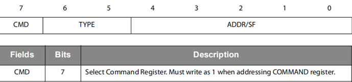
The manual tells us that the highest bit of the sending command must be 1. To address, this bit must be set to 1, that is, when sending the register address to be operated, we must set MSB to 1. So:
Usually, the header of the command register is 0x80
The register address should be 0x80|Address
With that in mind, we can start writing code.
#define TCS34725_ADDRESS          (0x29)

#define TCS34725_COMMAND_BIT      (0x80)

#define TCS34725_ENABLE           (0x00)
#define TCS34725_ENABLE_AIEN      (0x10)    /* RGBC Interrupt Enable */
#define TCS34725_ENABLE_WEN       (0x08)    /* Wait enable - Writing 1 activates the wait timer */
#define TCS34725_ENABLE_AEN       (0x02)    /* RGBC Enable - Writing 1 actives the ADC, 0 disables it */
#define TCS34725_ENABLE_PON       (0x01)    /* Power on - Writing 1 activates the internal oscillator, 0 disables it */
#define TCS34725_ATIME            (0x01)    /* Integration time */
#define TCS34725_WTIME            (0x03)    /* Wait time (if TCS34725_ENABLE_WEN is asserted) */
#define TCS34725_WTIME_2_4MS      (0xFF)    /* WLONG0 = 2.4ms   WLONG1 = 0.029s */
#define TCS34725_WTIME_204MS      (0xAB)    /* WLONG0 = 204ms   WLONG1 = 2.45s  */
#define TCS34725_WTIME_614MS      (0x00)    /* WLONG0 = 614ms   WLONG1 = 7.4s   */
#define TCS34725_AILTL            (0x04)    /* Clear channel lower interrupt threshold */
#define TCS34725_AILTH            (0x05)
#define TCS34725_AIHTL            (0x06)    /* Clear channel upper interrupt threshold */
#define TCS34725_AIHTH            (0x07)
#define TCS34725_PERS             (0x0C)    /* Persistence register - basic SW filtering mechanism for interrupts */
#define TCS34725_PERS_NONE        (0b0000)  /* Every RGBC cycle generates an interrupt                                */
#define TCS34725_PERS_1_CYCLE     (0b0001)  /* 1 clean channel value outside threshold range generates an interrupt   */
#define TCS34725_PERS_2_CYCLE     (0b0010)  /* 2 clean channel values outside threshold range generates an interrupt  */
#define TCS34725_PERS_3_CYCLE     (0b0011)  /* 3 clean channel values outside threshold range generates an interrupt  */
#define TCS34725_PERS_5_CYCLE     (0b0100)  /* 5 clean channel values outside threshold range generates an interrupt  */
#define TCS34725_PERS_10_CYCLE    (0b0101)  /* 10 clean channel values outside threshold range generates an interrupt */
#define TCS34725_PERS_15_CYCLE    (0b0110)  /* 15 clean channel values outside threshold range generates an interrupt */
#define TCS34725_PERS_20_CYCLE    (0b0111)  /* 20 clean channel values outside threshold range generates an interrupt */
#define TCS34725_PERS_25_CYCLE    (0b1000)  /* 25 clean channel values outside threshold range generates an interrupt */
#define TCS34725_PERS_30_CYCLE    (0b1001)  /* 30 clean channel values outside threshold range generates an interrupt */
#define TCS34725_PERS_35_CYCLE    (0b1010)  /* 35 clean channel values outside threshold range generates an interrupt */
#define TCS34725_PERS_40_CYCLE    (0b1011)  /* 40 clean channel values outside threshold range generates an interrupt */
#define TCS34725_PERS_45_CYCLE    (0b1100)  /* 45 clean channel values outside threshold range generates an interrupt */
#define TCS34725_PERS_50_CYCLE    (0b1101)  /* 50 clean channel values outside threshold range generates an interrupt */
#define TCS34725_PERS_55_CYCLE    (0b1110)  /* 55 clean channel values outside threshold range generates an interrupt */
#define TCS34725_PERS_60_CYCLE    (0b1111)  /* 60 clean channel values outside threshold range generates an interrupt */
#define TCS34725_CONFIG           (0x0D)
#define TCS34725_CONFIG_WLONG     (0x02)    /* Choose between short and long (12x) wait times via TCS34725_WTIME */
#define TCS34725_CONTROL          (0x0F)    /* Set the gain level for the sensor */
#define TCS34725_ID               (0x12)    /* 0x44 = TCS34721/TCS34725, 0x4D = TCS34723/TCS34727 */
#define TCS34725_STATUS           (0x13)
#define TCS34725_STATUS_AINT      (0x10)    /* RGBC Clean channel interrupt */
#define TCS34725_STATUS_AVALID    (0x01)    /* Indicates that the RGBC channels have completed an integration cycle */
#define TCS34725_CDATAL           (0x14)    /* Clear channel data */
#define TCS34725_CDATAH           (0x15)
#define TCS34725_RDATAL           (0x16)    /* Red channel data */
#define TCS34725_RDATAH           (0x17)
#define TCS34725_GDATAL           (0x18)    /* Green channel data */
#define TCS34725_GDATAH           (0x19)
#define TCS34725_BDATAL           (0x1A)    /* Blue channel data */
#define TCS34725_BDATAH           (0x1B)

#define TCS34725_INTEGRATIONTIME_2_4MS   0xFF   /**<  2.4ms - 1 cycle    - Max Count: 1024  */
#define TCS34725_INTEGRATIONTIME_24MS    0xF6   /**<  24ms  - 10 cycles  - Max Count: 10240 */
#define TCS34725_INTEGRATIONTIME_50MS    0xEB   /**<  50ms  - 20 cycles  - Max Count: 20480 */
#define TCS34725_INTEGRATIONTIME_101MS   0xD5   /**<  101ms - 42 cycles  - Max Count: 43008 */
#define TCS34725_INTEGRATIONTIME_154MS   0xC0   /**<  154ms - 64 cycles  - Max Count: 65535 */
#define TCS34725_INTEGRATIONTIME_240MS   0x9C   /**<  240ms - 100 cycles - Max Count: 65535 */
#define TCS34725_INTEGRATIONTIME_700MS   0x00   /**<  700ms - 256 cycles - Max Count: 65535 */

#define TCS34725_GAIN_1X                 0x00   /**<  No gain  */
#define TCS34725_GAIN_4X                 0x01   /**<  4x gain  */
#define TCS34725_GAIN_16X                0x02   /**<  16x gain */
#define TCS34725_GAIN_60X                0x03   /**<  60x gain */

#define max3v(v1, v2, v3)   ((v1)<(v2)? ((v2)<(v3)?(v3):(v2)):((v1)<(v3)?(v3):(v1)))
#define min3v(v1, v2, v3)   ((v1)>(v2)? ((v2)>(v3)?(v3):(v2)):((v1)>(v3)?(v3):(v1)))

//Two structures declared by. h file
typedef struct{
	unsigned short  c;      //[0-65536]
	unsigned short  r;
	unsigned short  g;
	unsigned short  b;
}COLOR_RGBC;//RGBC

/*******************************************************************************
 * @brief Writes data to a slave device.
 *
 * @param slaveAddress - Adress of the slave device.
 * @param dataBuffer - Pointer to a buffer storing the transmission data.
 * @param bytesNumber - Number of bytes to write.
 * @param stopBit - Stop condition control.
 *                  Example: 0 - A stop condition will not be sent;
 *                           1 - A stop condition will be sent.
*******************************************************************************/
void TCS34725_I2C_Write(uint8_t slaveAddress, uint8_t* dataBuffer,uint8_t bytesNumber, uint8_t stopBit)
{
	uint8_t i = 0;

	TCS34725_I2C_Start();
	TCS34725_I2C_Send_Byte((slaveAddress << 1) | 0x00);	   //Send slave address write command
	TCS34725_I2C_Wait_ACK();
	for(i = 0; i < bytesNumber; i++)
	{
		TCS34725_I2C_Send_Byte(*(dataBuffer + i));
		TCS34725_I2C_Wait_ACK();
	}
	if(stopBit == 1) TCS34725_I2C_Stop();
}
/*******************************************************************************
 * @brief Reads data from a slave device.
 *
 * @param slaveAddress - Adress of the slave device.
 * @param dataBuffer - Pointer to a buffer that will store the received data.
 * @param bytesNumber - Number of bytes to read.
 * @param stopBit - Stop condition control.
 *                  Example: 0 - A stop condition will not be sent;
 *                           1 - A stop condition will be sent.
*******************************************************************************/
void TCS34725_I2C_Read(uint8_t slaveAddress, uint8_t* dataBuffer, uint8_t bytesNumber, uint8_t stopBit)
{
	uint8_t i = 0;

	TCS34725_I2C_Start();
	TCS34725_I2C_Send_Byte((slaveAddress << 1) | 0x01);	   //Send slave address read command
	TCS34725_I2C_Wait_ACK();
	for(i = 0; i < bytesNumber; i++)
	{
		if(i == bytesNumber - 1)
		{
			*(dataBuffer + i) = TCS34725_I2C_Read_Byte(0);//Send NACK for the last byte read
		}
		else
		{
			*(dataBuffer + i) = TCS34725_I2C_Read_Byte(1);
		}
	}
	if(stopBit == 1) TCS34725_I2C_Stop();
}
/*******************************************************************************
 * @brief Writes data into TCS34725 registers, starting from the selected
 *        register address pointer.
 *
 * @param subAddr - The selected register address pointer.
 * @param dataBuffer - Pointer to a buffer storing the transmission data.
 * @param bytesNumber - Number of bytes that will be sent.
 *
 * @return None.
*******************************************************************************/
void TCS34725_Write(uint8_t subAddr, uint8_t* dataBuffer, uint8_t bytesNumber)
{
    uint8_t sendBuffer[10] = {0, };
    uint8_t byte = 0;

    sendBuffer[0] = subAddr | TCS34725_COMMAND_BIT;
    for(byte = 1; byte <= bytesNumber; byte++)
    {
        sendBuffer[byte] = dataBuffer[byte - 1];
    }
	TCS34725_I2C_Write(TCS34725_ADDRESS, sendBuffer, bytesNumber + 1, 1);
}
/*******************************************************************************
 * @brief Reads data from TCS34725 registers, starting from the selected
 *        register address pointer.
 *
 * @param subAddr - The selected register address pointer.
 * @param dataBuffer - Pointer to a buffer that will store the received data.
 * @param bytesNumber - Number of bytes that will be read.
 *
 * @return None.
*******************************************************************************/
void TCS34725_Read(uint8_t subAddr, uint8_t* dataBuffer, uint8_t bytesNumber)
{
	subAddr |= TCS34725_COMMAND_BIT;

	TCS34725_I2C_Write(TCS34725_ADDRESS, (uint8_t*)&subAddr, 1, 0);
	TCS34725_I2C_Read(TCS34725_ADDRESS, dataBuffer, bytesNumber, 1);
}
/*******************************************************************************
 * @brief TCS34725 Set integration time
 *
 * @return None
*******************************************************************************/
void TCS34725_SetIntegrationTime(uint8_t time)
{
	TCS34725_Write(TCS34725_ATIME, &time, 1);
}
/*******************************************************************************
 * @brief TCS34725 Set gain
 *
 * @return None
*******************************************************************************/
void TCS34725_SetGain(uint8_t gain)
{
	TCS34725_Write(TCS34725_CONTROL, &gain, 1);
}
/*******************************************************************************
 * @brief TCS34725 Enable
 *
 * @return None
*******************************************************************************/
void TCS34725_Enable(void)
{
	uint8_t cmd = TCS34725_ENABLE_PON;

	TCS34725_Write(TCS34725_ENABLE, &cmd, 1);
	cmd = TCS34725_ENABLE_PON | TCS34725_ENABLE_AEN;
	TCS34725_Write(TCS34725_ENABLE, &cmd, 1);
	//delay_s(600000);//delay_ms(3);// The delay should be placed after setting AEN
}
/*******************************************************************************
 * @brief TCS34725 Disability
 *
 * @return None
*******************************************************************************/
void TCS34725_Disable(void)
{
	uint8_t cmd = 0;

	TCS34725_Read(TCS34725_ENABLE, &cmd, 1);
	cmd = cmd & ~(TCS34725_ENABLE_PON | TCS34725_ENABLE_AEN);
	TCS34725_Write(TCS34725_ENABLE, &cmd, 1);
}
/*******************************************************************************
 * @brief TCS34725 initialization
 *
 * @return ID - ID Value in register
*******************************************************************************/
uint8_t TCS34725_Init(void)
{
	uint8_t id=0;

	//TCS34725_I2C_Init();
	TCS34725_Read(TCS34725_ID, &id, 1);  //The ID of TCS34725 is 0x44, which can be used to judge whether the connection is successful
	if(id==0x44)
		{
			TCS34725_SetIntegrationTime(TCS34725_INTEGRATIONTIME_240MS);
			TCS34725_SetGain(TCS34725_GAIN_1X);
			TCS34725_Enable();
			return 1;
		}
	return 0;
}
/*******************************************************************************
 * @brief TCS34725 Get single channel data
 *
 * @return data - Conversion value of this channel
*******************************************************************************/
uint16_t TCS34725_GetChannelData(uint8_t reg)
{
	uint8_t tmp[2] = {0,0};
	uint16_t data;

	TCS34725_Read(reg, tmp, 2);
	data = (tmp[1] << 8) | tmp[0];

	return data;
}
/*******************************************************************************
 * @brief TCS34725 Obtain data of each channel
 *
 * @return 1 - The conversion is complete and the data is available
 *   	   0 - Conversion not completed, data not available
*******************************************************************************/
uint8_t TCS34725_GetRawData(COLOR_RGBC *rgbc)
{
	uint8_t status = TCS34725_STATUS_AVALID;

	TCS34725_Read(TCS34725_STATUS, &status, 1);

	if(status & TCS34725_STATUS_AVALID)
	{
		rgbc->c = TCS34725_GetChannelData(TCS34725_CDATAL);
		rgbc->r = TCS34725_GetChannelData(TCS34725_RDATAL);
		rgbc->g = TCS34725_GetChannelData(TCS34725_GDATAL);
		rgbc->b = TCS34725_GetChannelData(TCS34725_BDATAL);
		return 1;
	}
	return 0;
}
Here, the driver of TSC34725 is completed. The data read here is unprocessed data. If you want to convert it into usable RGB, you can convert it.