Analysis of one click download principle of P3 serial port circuit
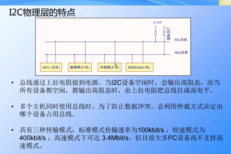
Pull up circuit
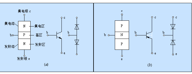
triode
b is the base, c is the collector and e is the emitter
When used as a switch, NPN triode: when b is connected to low level, the circuit is cut off, and when b is connected to high level, the circuit is saturated and on; PNP triode: if b is connected to high level, the circuit is cut off, and if b is connected to low level, the circuit is saturated and on
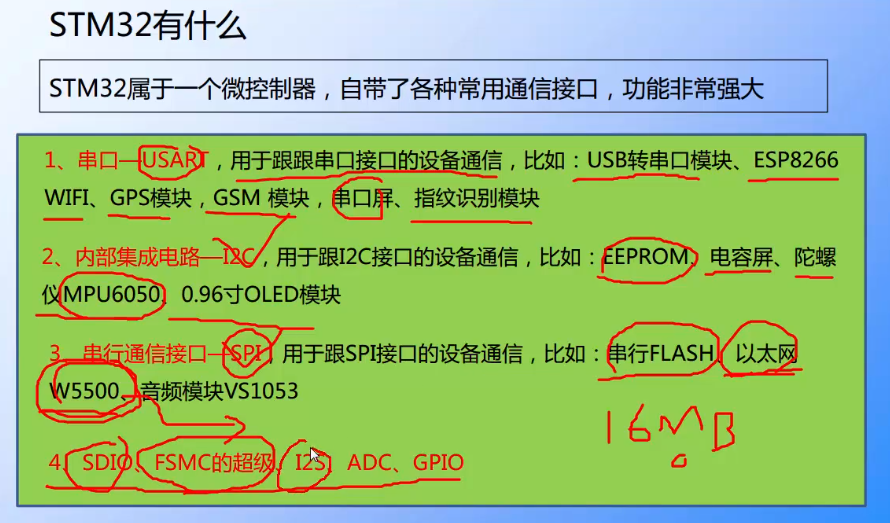
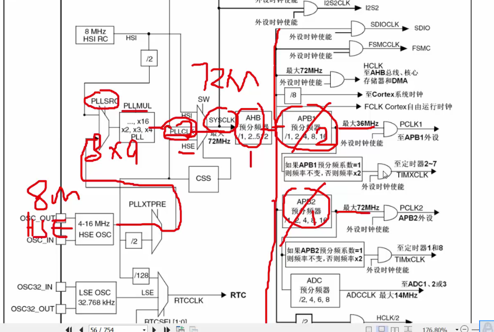
GPIO: general input and output
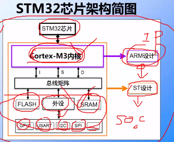
P5 first acquaintance with STM32
Shenzhen jialichuang Co., Ltd. is selected for PCB proofing
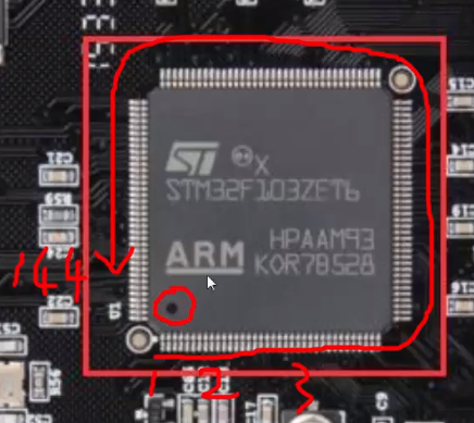
Pin sequence: rotate counterclockwise from the black dot to the positive direction
The written program is compiled and stored in FLASH. If the kernel wants to read these instructions to execute the program, it must pass through ICode bus
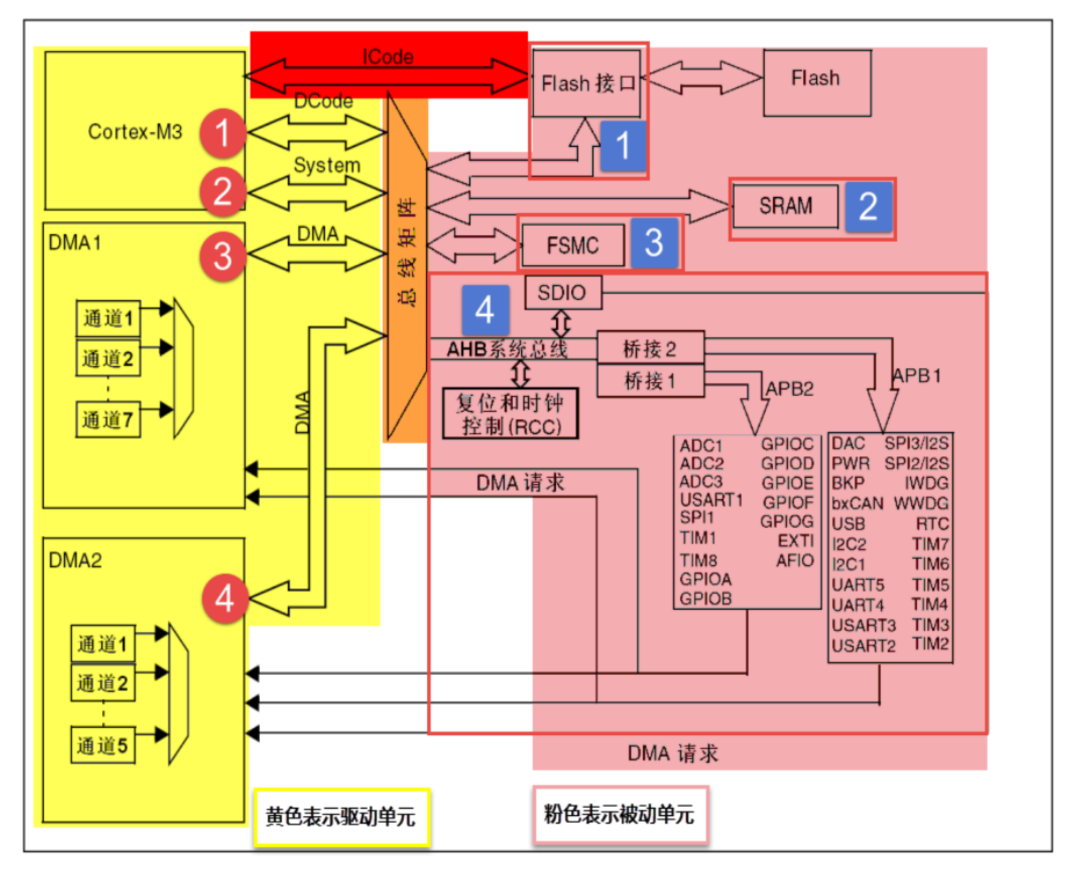
FLASH is used to store programs
SRAM is used to store variables
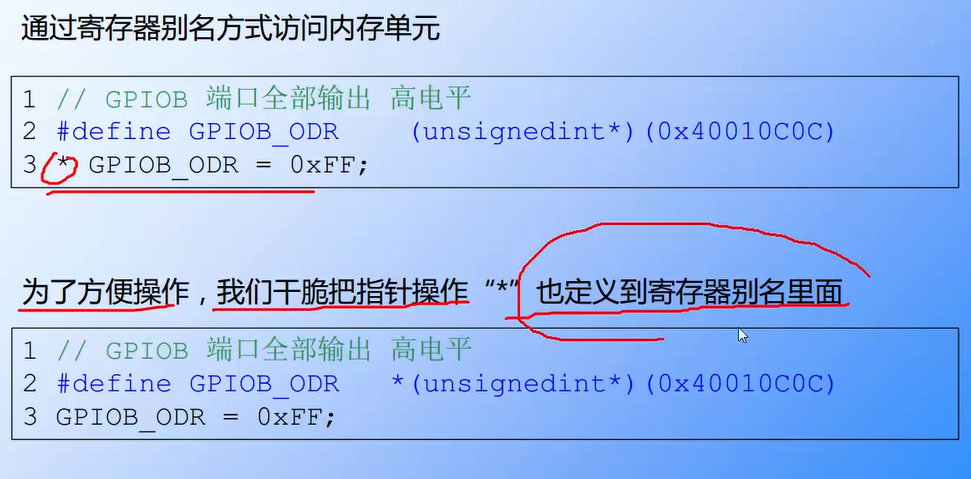
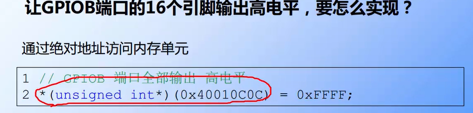 (unsigned int *) cast address
*+The address unit can operate the data in the address

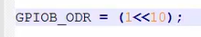
 This code means that 1 shifts 10 bits to the left, and the others are set to 0, that is, the 10th position is 1, and the other bits are set to 0
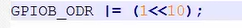
|=Or equal, that is, the 10th bit is 1, and the other bits are 0, which is the phase or of the original, and then assigned to the original set, that is, the 10th position is 1, and the other bits remain unchanged

The operation will be reversed, equal to the other bit, & =, and the same as the other bit

The angle brackets in the header file indicate that the header file is not in the directory of the current project, but in the directory of the compiler
The "" in the header file indicates that the header file is in the directory of the current project. If it cannot be found in the directory of the current project, go to the compiler directory.
32-bit register, each register has 32 bits
P7 illuminates an LED
#include"stm32f10x.h"


int main (void)
{
	///Open the clock of GPIOB port
	*(unsigned int*)0x40021018 |=(1<<3);
	//Configure IO port as output
	*(unsigned int*)0x40010C00 |= (1<<(4*5));//The first position bit in 0x40010C00 address is 1
	//Control ODR register
	*(unsigned int*)0x40010C0C &= ~(1<<0);//Cannot directly 0x40010C0C & = ~ (1 < < 0); The compiler will treat it as an immediate number. The first position of 0x40010C0C is 0
}


//Set | =, clear 0&=

void SystemInit(void)
{
	//The function body is empty in order to deceive the compiler not to report an error
}
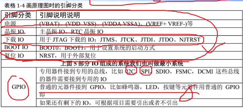
P8 explanation of GPIO function block diagram (key points)
GPIO: general purpose input output
Basic structure of IO port bit
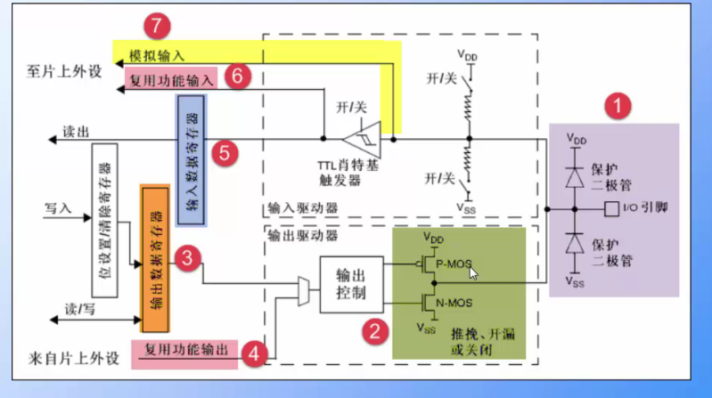
Parts 1-4 are output and parts 5-7 are input
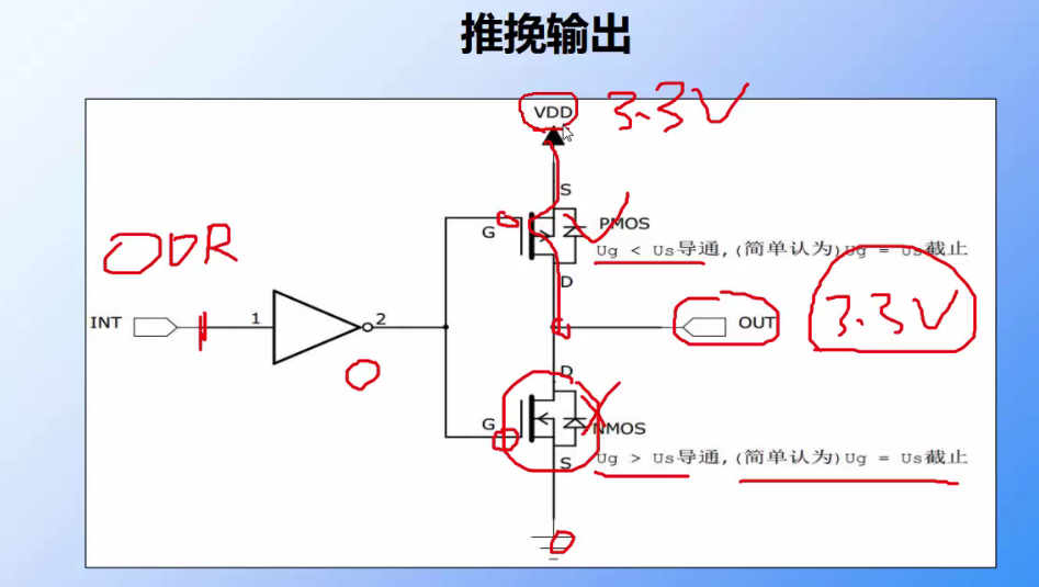
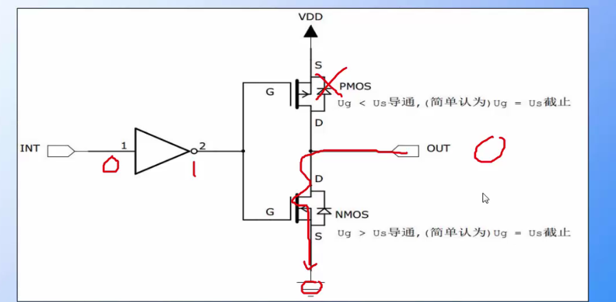
Part 1 bit protection circuit: when the voltage of I/O pin is too high, it enters VDD (3.3V voltage) through the upper transistor. When the voltage is too low (negative value), it is protected through the lower circuit Vss (grounding)
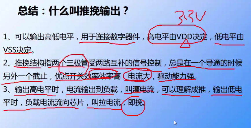
Part 2 bit push-pull output circuit,
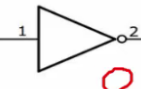 For inverter, input 1 will output 0, input 0 will output 1
 Open drain output: it can only output low level, not high level. It needs an additional pull-up circuit to output high level
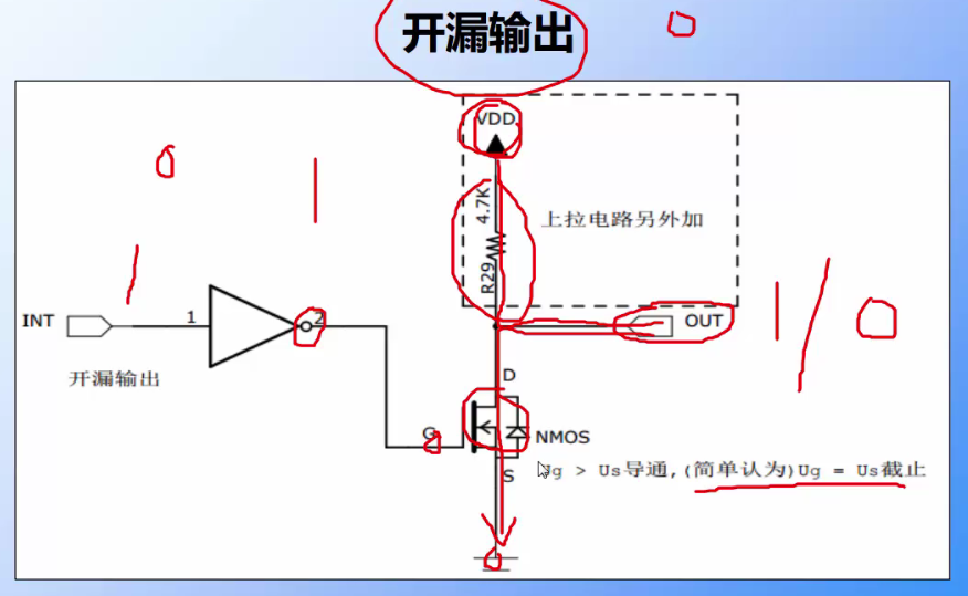
The open drain circuit is generally used on the I-side C or SM bus
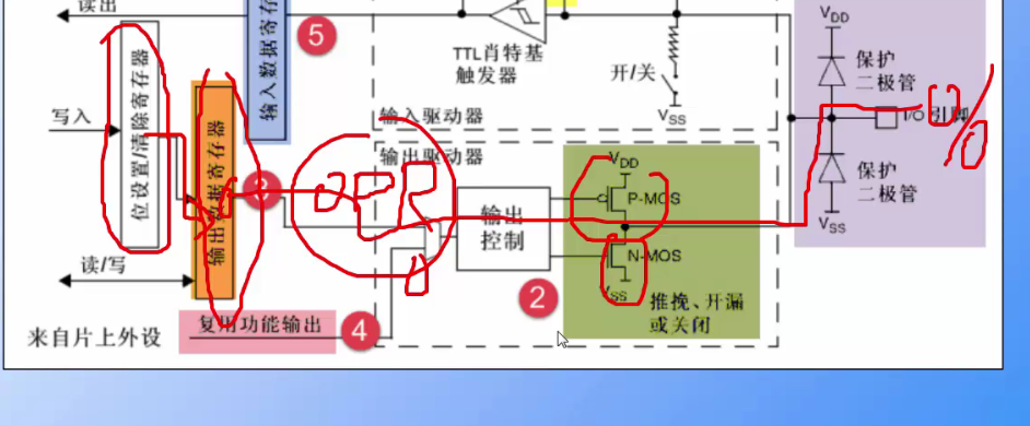
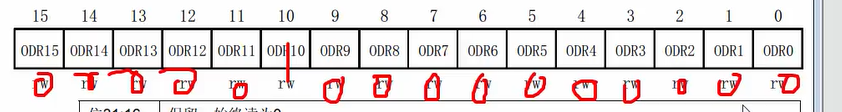
In part 3, the output data register (ODR) can directly control the output to high level or low level, or control the output data register to indirectly output high level or low level through bit set / clear register (BSRR)
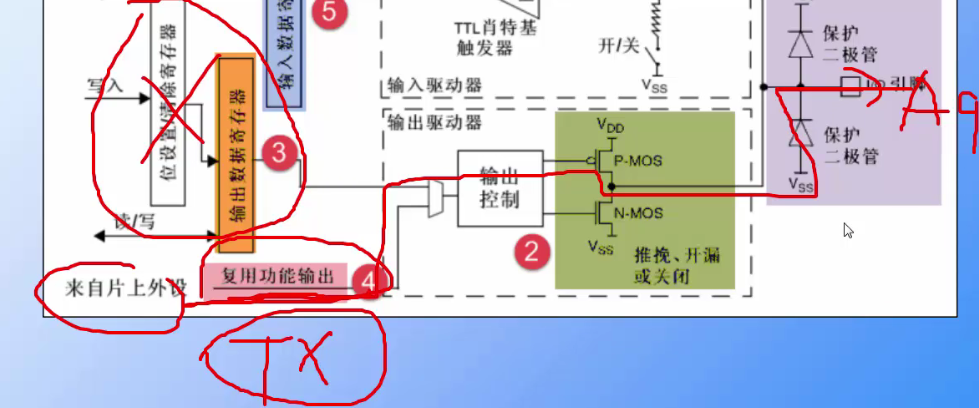
Part 4, multiplexing function output. When using this function, Part 3 will not work. The output of the pin is controlled through the on-chip peripheral (serial port)
Part 5 is the input data register (IDR), which can read the data of external pins and the data in ODR
The pull-up circuit and pull-down circuit set the pull-up / pull-down input mode through the port configuration low register (CRL)
The specific pull-up or pull-down can be controlled by software through the port bit setting / clearing register (BSRR)
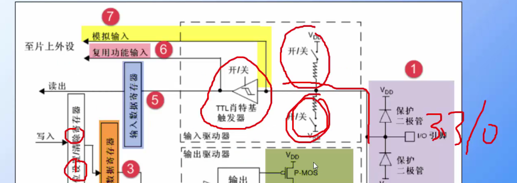
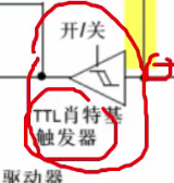
Schottky trigger is equivalent to access control. When the input level is greater than 2.0V, it is high level, and when the input level is Xiaoyu 1.2V, it is low level
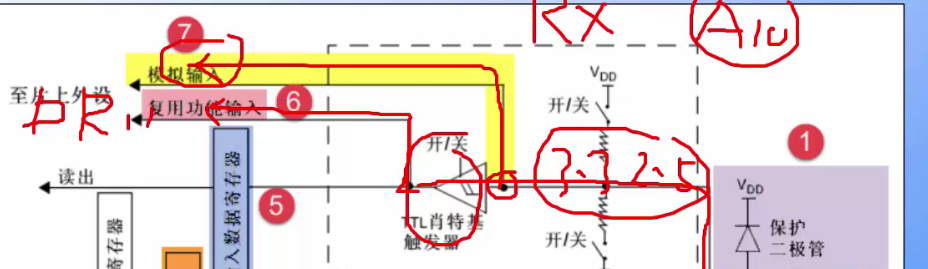
Part 6 multiplexing function input is input from on-chip peripherals,
Part 7 analog input directly collects analog signals without Schottky trigger processing
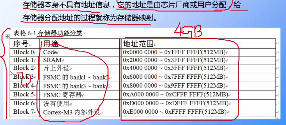
Direct programming of memory

stm32f10x.h code in file
//Code used to store STM32 register mapping


//Peripheral philippiral

#define PHERIPH_BASE        ((unsigned int)0x40000000)
#define APB1PHERIPH_BASE            PHERIPH_BASE
#define APB2PHERIPH_BASE           (PHERIPH_BASE + 0x10000)
#define AHBPHERIPH_BASE            (PHERIPH_BASE + 0x20000)


#define RCC_BASE            (AHBPHERIPH_BASE + 0x1000)
#define  GPIOB_BASE         (APB2PHERIPH_BASE + 0x0C00)

#define RCC_APB2ENR          *(unsigned int*)(RCC_BASE + 0x18)

#define GPIOB_CRL            *(unsigned int*)(GPIOB_BASE + 0x00)
#define GPIOB_CRH            *(unsigned int*)(GPIOB_BASE + 0x04)
#define GPIOB_ODR            *(unsigned int*)(GPIOB_BASE + 0x0C)
#define GPIOB_BSRR            *(unsigned int*)(GPIOB_BASE + 0x10)
#define GPIOB_BRR            *(unsigned int*)(GPIOB_BASE + 0x14)
Code in main,c file
#include "stm32f10x.h"


int main (void)
{
#if 0
	///Open the clock of GPIOB port
	*(unsigned int*)0x40021018 |=(1<<3);
	//Configure IO port as output
	*(unsigned int*)0x40010C00 &= ~((0x0f)<<(4*5));//Clear the register first
	*(unsigned int*)0x40010C00 |= (1<<(4*5));//The first position bit in 0x40010C00 address is 1
	//Control ODR register
	*(unsigned int*)0x40010C0C &= ~(1<<5);//Cannot directly 0x40010C0C & = ~ (1 < < 0); The compiler will treat it as an immediate number. The first position of 0x40010C0C is 0
#else
		///Open the clock of GPIOB port
	RCC_APB2ENR  |=(1<<3);
	//Configure IO port as output
	GPIOB_CRL &= ~((0x0f)<<(4*1));
	GPIOB_CRL |= (1<<(4*1));
	//Control the ODR register to directly control the output
	//GPIOB_ODR |= (1<<1);
	//Control the BSRR register to indirectly control the output
	GPIOB_BSRR &= ~(1<<1);
#endif
}


//Set | =, clear 0&=

void SystemInit(void)
{
	//The function body is empty in order to deceive the compiler not to report an error
}
P12 # write your own library - build library functions
The register is controlled by structure
First define a structure (GPIO_TypeDef in the example), the type and distribution order of the members of the structure are the same as that of the peripheral registers (GPIOB register in the example program), and then find the base address of the peripheral, such as GPIOB in the program_ Base, and then cast the address to GPIO_ Typedef is a pointer of this structure type. After forced type conversion, this pointer will point to all registers of the peripheral. The structure plus pointer can point to the register of the peripheral.
stm32f10x.h code in file
//Code used to store STM32 register mapping


//Peripheral philippiral

#define PHERIPH_BASE        ((unsigned int)0x40000000)
#define APB1PHERIPH_BASE            PHERIPH_BASE
#define APB2PHERIPH_BASE           (PHERIPH_BASE + 0x10000)
#define AHBPHERIPH_BASE            (PHERIPH_BASE + 0x20000)


#define RCC_BASE            (AHBPHERIPH_BASE + 0x1000)
#define  GPIOB_BASE         (APB2PHERIPH_BASE + 0x0C00)

#define RCC_APB2ENR          *(unsigned int*)(RCC_BASE + 0x18)

//#define GPIOB_CRL            *(unsigned int*)(GPIOB_BASE + 0x00)
//#define GPIOB_CRH            *(unsigned int*)(GPIOB_BASE + 0x04)
//#define GPIOB_IDR            *(unsigned int*)(GPIOB_BASE + 0x08)
//#define GPIOB_ODR            *(unsigned int*)(GPIOB_BASE + 0x0C)
//#define GPIOB_BSRR            *(unsigned int*)(GPIOB_BASE + 0x10)
//#define GPIOB_BRR            *(unsigned int*)(GPIOB_BASE + 0x14)
//#define GPIOB_LCKR            *(unsigned int*)(GPIOB_BASE + 0x18)

typedef unsigned int     uint32_t;
typedef unsigned short   uint16_t;

typedef struct
{
	uint32_t CR;
	uint32_t CFGR;
	uint32_t CIR;
	uint32_t APB2RSTR;
	uint32_t APB1RSTR;
	uint32_t AHBENR;
	uint32_t APB2ENR;
	uint32_t APB1ENR;
	uint32_t BDCR;
	uint32_t CSR;
}RCC_TypeDef;
#define  RCC  ((RCC_TypeDef*)RCC_BASE) / / cast type


typedef struct
{
	uint32_t CRL;
	uint32_t CRH;
	uint32_t IDR;
	uint32_t ODR;
	uint32_t BSRR;
	uint32_t BRR;
	uint32_t LCKR;
}GPIO_TypeDef;

#define GPIOB  ((GPIO_TypeDef*)GPIOB_BASE) / / cast type
Code in main,c file
#include "stm32f10x.h"


int main (void)
{

    ///Open the clock of GPIOB port
	RCC->APB2ENR  |=(1<<3);
	//Configure IO port as output
	GPIOB->CRL &= ~((0x0f)<<(4*1));
	GPIOB->CRL |= (1<<(4*1));
	//Control the ODR register to directly control the output
	//GPIOB_ODR |= (1<<1);
	//Control the BSRR register to indirectly control the output
	GPIOB->BSRR &= ~(1<<1);
#endif
}


//Set | =, clear 0&=

void SystemInit(void)
{
	//The function body is empty in order to deceive the compiler not to report an error
}

}
In order to avoid the error warning caused by multiple calls to the header file, a few statements can be added at the beginning and end of the header file
start
#ifndef __STM3210X_H / / the header file name is stm32f10x h. Then the code here is correct__ STM3210X_H macro definition
#define __STM3210X_H / / ditto
ending
#endif /*__STM3210X_H*/
Define functions to control registers
To increase the readability of the program, the port set and reset functions are defined to control the output of the port


#ifndef __STM32F10X_GPIO_H
#define __STM32F10X_GPIO_H

#include "stm32f10x.h"

#define GPIO_ Pin_ 0      ((uint16_t)0x0001) /*!< Select Pin0 */ //(00000000 00000001)b
#define GPIO_ Pin_ 1      ((uint16_t)0x0002) /*!< Select Pin1 */ //(00000000 00000010)b
#define GPIO_ Pin_ 2      ((uint16_t)0x0004) /*!< Select Pin2 */ //(00000000 00000100)b
#define GPIO_ Pin_ 3      ((uint16_t)0x0008) /*!< Select Pin3 */ //(00000000 00001000)b
#define GPIO_ Pin_ 4      ((uint16_t)0x0010) /*!< Select Pin4 */ //(00000000 00010000)b
#define GPIO_ Pin_ 5      ((uint16_t)0x0020) /*!< Select Pin5 */ //(00000000 00100000)b
#define GPIO_ Pin_ 6      ((uint16_t)0x0040) /*!< Select Pin6 */ //(00000000 01000000)b
#define GPIO_ Pin_ 7      ((uint16_t)0x0080) /*!< Select pin7 * / / / (000000 10000000) B

#define GPIO_ Pin_ 8       ((uint16_t)0x0100) /*!< Select Pin8 */ //(00000001 00000000)b
#define GPIO_ Pin_ 9       ((uint16_t)0x0200) /*!< Select Pin9 */ //(00000010 00000000)b
#define GPIO_ Pin_ 10      ((uint16_t)0x0400) /*!< Select Pin10 */ //(00000100 00000000)b
#define GPIO_ Pin_ 11      ((uint16_t)0x0800) /*!< Select pin11 * / / / (00001000000000) B
#define GPIO_ Pin_ 12      ((uint16_t)0x1000) /*!< Select Pin12 */ //(00010000 00000000)b
#define GPIO_ Pin_ 13      ((uint16_t)0x2000) /*!< Select Pin13 */ //(00100000 00000000)b
#define GPIO_ Pin_ 14      ((uint16_t)0x4000) /*!< Select Pin14 */ //(01000000 00000000)b
#define GPIO_ Pin_ 15      ((uint16_t)0x8000) /*!< / / (pin1000) select
#define GPIO_ Pin_ All      ((uint16_t)0x0001) /*!< Select all pins * / / / (11111111111) B

void GPIO_SetBits(GPIO_TypeDef *GPIOx,uint16_t GPIO_Pin);
void GPIO_ResetBits(GPIO_TypeDef *GPIOx,uint16_t GPIO_Pin);
#endif /* __STM32F10X_GPIO_H*/

#include "stm32f10x_gpio.h"
void GPIO_SetBits(GPIO_TypeDef *GPIOx,uint16_t GPIO_Pin)
{
	GPIOx->BSRR |= GPIO_Pin;//Control BSRR register
}

void GPIO_ResetBits(GPIO_TypeDef *GPIOx,uint16_t GPIO_Pin)
{
	GPIOx->BRR |= GPIO_Pin;//Control BRR register
}

#include "stm32f10x.h"
#include "stm32f10x_gpio.h"

int main (void)
{

	///Open the clock of GPIOB port
	RCC->APB2ENR  |=(1<<3);
	//Configure IO port as output
	GPIOB->CRL &= ~((0x0f)<<(4*0));
	GPIOB->CRL |= (1<<(4*0));

	GPIO_SetBits(GPIOB,GPIO_Pin_0);//Set the PB0 port, that is, call the function control to turn off the LED
	GPIO_ResetBits(GPIOB,GPIO_Pin_0);//Reset the PB0 port, that is, call the function to turn on the LED
#endif
}


//Set | =, clear 0&=

void SystemInit(void)
{
	//The function body is empty in order to deceive the compiler not to report an error
}

#ifndef __STM3210X_H
#define __STM3210X_H
//Code used to store STM32 register mapping


//Peripheral philippiral

#define PHERIPH_BASE        ((unsigned int)0x40000000)
#define APB1PHERIPH_BASE            PHERIPH_BASE
#define APB2PHERIPH_BASE           (PHERIPH_BASE + 0x10000)
#define AHBPHERIPH_BASE            (PHERIPH_BASE + 0x20000)


#define RCC_BASE            (AHBPHERIPH_BASE + 0x1000)
#define  GPIOB_BASE         (APB2PHERIPH_BASE + 0x0C00)

#define RCC_APB2ENR          *(unsigned int*)(RCC_BASE + 0x18)


typedef unsigned int     uint32_t;
typedef unsigned short   uint16_t;

typedef struct
{
	uint32_t CR;
	uint32_t CFGR;
	uint32_t CIR;
	uint32_t APB2RSTR;
	uint32_t APB1RSTR;
	uint32_t AHBENR;
	uint32_t APB2ENR;
	uint32_t APB1ENR;
	uint32_t BDCR;
	uint32_t CSR;
}RCC_TypeDef;
#define  RCC  ((RCC_TypeDef*)RCC_BASE)

typedef struct
{
	uint32_t CRL;
	uint32_t CRH;
	uint32_t IDR;
	uint32_t ODR;
	uint32_t BSRR;
	uint32_t BRR;
	uint32_t LCKR;
}GPIO_TypeDef;

#define GPIOB  ((GPIO_TypeDef*)GPIOB_BASE)


#endif /*__STM3210X_H*/
The structure and initialization function are used for initialization
The definition of variables in C language should be placed at the beginning, not in the middle of the program, otherwise an error will be reported
The purpose of writing initialization function in the tutorial is to make the program more readable. You can understand what the program needs to do without looking up the reference manual
Step: define an initialization structure of the peripheral, enumerate all the parameters (speed, mode, etc.) of the registers that can be configured. When programming, you can write the parameters defined in the enumeration to the initialized structure, and finally call the initialization function of the peripheral to write the members configured in the structure to the corresponding registers. Realize the work of configuration register.


#ifndef __STM32F10X_GPIO_H
#define __STM32F10X_GPIO_H

#include "stm32f10x.h"

#define GPIO_ Pin_ 0      ((uint16_t)0x0001) /*!< Select Pin0 */ //(00000000 00000001)b
#define GPIO_ Pin_ 1      ((uint16_t)0x0002) /*!< Select Pin1 */ //(00000000 00000010)b
#define GPIO_ Pin_ 2      ((uint16_t)0x0004) /*!< Select Pin2 */ //(00000000 00000100)b
#define GPIO_ Pin_ 3      ((uint16_t)0x0008) /*!< Select Pin3 */ //(00000000 00001000)b
#define GPIO_ Pin_ 4      ((uint16_t)0x0010) /*!< Select Pin4 */ //(00000000 00010000)b
#define GPIO_ Pin_ 5      ((uint16_t)0x0020) /*!< Select Pin5 */ //(00000000 00100000)b
#define GPIO_ Pin_ 6      ((uint16_t)0x0040) /*!< Select Pin6 */ //(00000000 01000000)b
#define GPIO_ Pin_ 7      ((uint16_t)0x0080) /*!< Select pin7 * / / / (000000 10000000) B

#define GPIO_ Pin_ 8       ((uint16_t)0x0100) /*!< Select Pin8 */ //(00000001 00000000)b
#define GPIO_ Pin_ 9       ((uint16_t)0x0200) /*!< Select Pin9 */ //(00000010 00000000)b
#define GPIO_ Pin_ 10      ((uint16_t)0x0400) /*!< Select Pin10 */ //(00000100 00000000)b
#define GPIO_ Pin_ 11      ((uint16_t)0x0800) /*!< Select pin11 * / / / (00001000000000) B
#define GPIO_ Pin_ 12      ((uint16_t)0x1000) /*!< Select Pin12 */ //(00010000 00000000)b
#define GPIO_ Pin_ 13      ((uint16_t)0x2000) /*!< Select Pin13 */ //(00100000 00000000)b
#define GPIO_ Pin_ 14      ((uint16_t)0x4000) /*!< Select Pin14 */ //(01000000 00000000)b
#define GPIO_ Pin_ 15      ((uint16_t)0x8000) /*!< Select pin15 * / / / (1000000000000) B
#define GPIO_ Pin_ All      ((uint16_t)0x0001) /*!< Select all pins * / / / (11111111111) B

typedef enum//enumeration
{
	GPIO_Speed_10MHZ = 1,       //10 MHZ     (01)b
	GPIO_Speed_2MHZ,            //2MHZ       (10)b
	GPIO_Speed_50MHZ            //50MHZ      (11)b
}GPIOSpeed_TypeDef;

typedef enum
{
	GPIO_Mode_AIN = 0x0,          //Analog input (0000) B
	GPIO_Mode_IN_FLOATING = 0x04, //Floating input (0000 0100)b
	GPIO_Mode_IPD = 0x28,         //Pull down input (0010 1000)b
	GPIO_Mode_IPU = 0x48,         //Pull up input (0100 1000)b

	GPIO_Mode_Out_OD = 0x14,      //Open drain output (0001 0100)b
	GPIO_Mode_Out_PP = 0x10,      //Push pull output (0001 0000)b
	GPIO_Mode_AF_OD = 0x1C,       //Multiplexed open drain output (0001 1100)b
	GPIO_Mode_AF_PP = 0x18,       //Multiplexed push-pull output (0001 1000)b
}GPIOMode_TypeDef;

typedef struct
{
	uint16_t GPIO_Pin;
	uint16_t GPIO_Speed;
	uint16_t GPIO_Mode;
}GPIO_InitTypeDef;

void GPIO_SetBits(GPIO_TypeDef *GPIOx,uint16_t GPIO_Pin);
void GPIO_ResetBits(GPIO_TypeDef *GPIOx,uint16_t GPIO_Pin);
void GPIO_Init(GPIO_TypeDef* GPIOx, GPIO_InitTypeDef* GPIO_InitStruct);
#endif /* __STM32F10X_GPIO_H*/

#include "stm32f10x_gpio.h"
void GPIO_SetBits(GPIO_TypeDef *GPIOx,uint16_t GPIO_Pin)
{
	GPIOx->BSRR |= GPIO_Pin;//Control BSRR register
}

void GPIO_ResetBits(GPIO_TypeDef *GPIOx,uint16_t GPIO_Pin)
{
	GPIOx->BRR |= GPIO_Pin;//Control BRR register
}

void GPIO_Init(GPIO_TypeDef* GPIOx, GPIO_InitTypeDef* GPIO_InitStruct)
{
  uint32_t currentmode = 0x00, currentpin = 0x00, pinpos = 0x00, pos = 0x00;
  uint32_t tmpreg = 0x00, pinmask = 0x00;

/*---------------------- GPIO Mode configuration--------------------------*/
  // Input parameter GPIO_ The lower four bits of mode are temporarily stored in currentmode
  currentmode = ((uint32_t)GPIO_InitStruct->GPIO_Mode) & ((uint32_t)0x0F);

  // Bit4 is 1 for output and bit4 is 0 for input
  // Judge whether bit4 is 1 or 0, that is, it is preferred to judge whether it is input or output mode
  if ((((uint32_t)GPIO_InitStruct->GPIO_Mode) & ((uint32_t)0x10)) != 0x00)
  {
	// In the output mode, the output speed should be set
    currentmode |= (uint32_t)GPIO_InitStruct->GPIO_Speed;
  }
/*-------------GPIO CRL Register configuration CRL register controls the low 8-bit IO --------*/
  // Configure the lower 8 bits of the port, i.e. Pin0~Pin7
  if (((uint32_t)GPIO_InitStruct->GPIO_Pin & ((uint32_t)0x00FF)) != 0x00)
  {
	// Back up the value of CRL register first
    tmpreg = GPIOx->CRL;

	// Loop, pairing from Pin0 to find out the specific Pin
    for (pinpos = 0x00; pinpos < 0x08; pinpos++)
    {
	 // The value of pos is 1. Shift the pinpos bit to the left
      pos = ((uint32_t)0x01) << pinpos;

	  // Make pos and input parameter GPIO_ The pin performs bit and operation to prepare for the following judgment
      currentpin = (GPIO_InitStruct->GPIO_Pin) & pos;

	  //If currentpin=pos, find the pin used
      if (currentpin == pos)
      {
		// The value of pinpos is shifted two bits to the left (multiplied by 4) because four register bits in the register configure one pin
        pos = pinpos << 2;
       //Clear the four register bits controlling this pin, and the other register bits remain unchanged
        pinmask = ((uint32_t)0x0F) << pos;
        tmpreg &= ~pinmask;

        // Write the mode of the pin to be configured to the register
        tmpreg |= (currentmode << pos);

		// Judge whether it is a pull-down input mode
        if (GPIO_InitStruct->GPIO_Mode == GPIO_Mode_IPD)
        {
		  // In the pull-down input mode, the pin is set to 0 by default. Writing 1 to the BRR register can set the pin to 0
          GPIOx->BRR = (((uint32_t)0x01) << pinpos);
        }
        else
        {
          // Judge whether it is pull-up input mode
          if (GPIO_InitStruct->GPIO_Mode == GPIO_Mode_IPU)
          {
		    // In the pull-up input mode, the default value of the pin is 1. Write 1 to the BSRR register and set the pin to 1
            GPIOx->BSRR = (((uint32_t)0x01) << pinpos);
          }
        }
      }
    }
		// Write the previously processed temporary value into the CRL register
    GPIOx->CRL = tmpreg;
  }
/*-------------GPIO CRH Register configuration CRH register controls the upper 8-bit IO ------------*/
  // Configure the upper 8 bits of the port, i.e. Pin8~Pin15
  if (GPIO_InitStruct->GPIO_Pin > 0x00FF)
  {
		// //Back up the value of CRH register first
    tmpreg = GPIOx->CRH;

	// Loop, start pairing from Pin8 and find out the specific Pin
    for (pinpos = 0x00; pinpos < 0x08; pinpos++)
    {
      pos = (((uint32_t)0x01) << (pinpos + 0x08));

      // pos and input parameter GPIO_PIN bit and operation
      currentpin = ((GPIO_InitStruct->GPIO_Pin) & pos);

	 //If currentpin=pos, find the pin used
      if (currentpin == pos)
      {
		//The value of pinpos is shifted two bits to the left (multiplied by 4) because four register bits in the register configure one pin
        pos = pinpos << 2;

	    //Clear the four register bits controlling this pin, and the other register bits remain unchanged
        pinmask = ((uint32_t)0x0F) << pos;
        tmpreg &= ~pinmask;

        // Write the mode of the pin to be configured to the register
        tmpreg |= (currentmode << pos);

		// Judge whether it is a pull-down input mode
        if (GPIO_InitStruct->GPIO_Mode == GPIO_Mode_IPD)
        {
		  // In the pull-down input mode, the pin is set to 0 by default. Writing 1 to the BRR register can set the pin to 0
          GPIOx->BRR = (((uint32_t)0x01) << (pinpos + 0x08));
        }
         // Judge whether it is pull-up input mode
        if (GPIO_InitStruct->GPIO_Mode == GPIO_Mode_IPU)
        {
		  // In the pull-up input mode, the default value of the pin is 1. Write 1 to the BSRR register and set the pin to 1
          GPIOx->BSRR = (((uint32_t)0x01) << (pinpos + 0x08));
        }
      }
    }
	// Write the previously processed temporary value into the CRH register
    GPIOx->CRH = tmpreg;
  }
}

#include "stm32f10x.h"
#include "stm32f10x_gpio.h"

int main (void)
{

	GPIO_InitTypeDef GPIO_InitStructure;//The definition of variables in C language should be placed at the beginning, not in the middle of the program, otherwise an error will be reported
		///Open the clock of GPIOB port
	RCC->APB2ENR  |=(1<<3);
	//Configure IO port as output

	GPIO_InitStructure.GPIO_Pin = GPIO_Pin_0;
	GPIO_InitStructure.GPIO_Mode = GPIO_Mode_Out_PP;
	GPIO_InitStructure.GPIO_Speed = GPIO_Speed_50MHZ;

	GPIO_Init(GPIOB, &GPIO_InitStructure);//&In order to get the address character, this is the address of the structure when defining the function, so when using the function, this is the address to call

	GPIO_SetBits(GPIOB,GPIO_Pin_0);//Call the function control to turn off the LED
	GPIO_ResetBits(GPIOB,GPIO_Pin_0);//Call the function to turn on the LED
#endif
}


//Set | =, clear 0&=

void SystemInit(void)
{
	//The function body is empty in order to deceive the compiler not to report an error
}

#ifndef __STM3210X_H
#define __STM3210X_H
//Code used to store STM32 register mapping


//Peripheral philippiral

#define PHERIPH_BASE        ((unsigned int)0x40000000)
#define APB1PHERIPH_BASE            PHERIPH_BASE
#define APB2PHERIPH_BASE           (PHERIPH_BASE + 0x10000)
#define AHBPHERIPH_BASE            (PHERIPH_BASE + 0x20000)


#define RCC_BASE            (AHBPHERIPH_BASE + 0x1000)
#define  GPIOB_BASE         (APB2PHERIPH_BASE + 0x0C00)

#define RCC_APB2ENR          *(unsigned int*)(RCC_BASE + 0x18)

//#define GPIOB_CRL            *(unsigned int*)(GPIOB_BASE + 0x00)
//#define GPIOB_CRH            *(unsigned int*)(GPIOB_BASE + 0x04)
//#define GPIOB_IDR            *(unsigned int*)(GPIOB_BASE + 0x08)
//#define GPIOB_ODR            *(unsigned int*)(GPIOB_BASE + 0x0C)
//#define GPIOB_BSRR            *(unsigned int*)(GPIOB_BASE + 0x10)
//#define GPIOB_BRR            *(unsigned int*)(GPIOB_BASE + 0x14)
//#define GPIOB_LCKR            *(unsigned int*)(GPIOB_BASE + 0x18)

typedef unsigned int     uint32_t;
typedef unsigned short   uint16_t;

typedef struct
{
	uint32_t CR;
	uint32_t CFGR;
	uint32_t CIR;
	uint32_t APB2RSTR;
	uint32_t APB1RSTR;
	uint32_t AHBENR;
	uint32_t APB2ENR;
	uint32_t APB1ENR;
	uint32_t BDCR;
	uint32_t CSR;
}RCC_TypeDef;
#define  RCC  ((RCC_TypeDef*)RCC_BASE)

typedef struct
{
	uint32_t CRL;
	uint32_t CRH;
	uint32_t IDR;
	uint32_t ODR;
	uint32_t BSRR;
	uint32_t BRR;
	uint32_t LCKR;
}GPIO_TypeDef;

#define GPIOB  ((GPIO_TypeDef*)GPIOB_BASE)


#endif /*__STM3210X_H*/
P10 firmware library programming
What files does the firmware library contain
1 - compilation of start-up documents
startup_stm32f10x_hd.s: Set stack pointer, set PC pointer, initialize interrupt vector table, configure system clock, and use C library functions_ main finally goes to the world of C
2 - clock profile
system_stm32f10x.c: Set the external clock HSE=8M to 72M after PLL frequency doubling.
3 - peripheral related
stm32f10x.h: The register mapping of peripherals outside the kernel is realized
xxx: GPIO,USRAT,I2C,SPI,FSMC
stm32f10x_xx.c: Peripheral driver library file
stm32f10x_xx.h: Store the initialization structure of the peripheral, the parameter list of the members of the initialization structure of the peripheral, and the declaration of the firmware library function of the peripheral
4 - kernel related
CMSIS - Cortex microcontroller software interface standard
core_cm3.h: The register mapping of peripherals in the kernel is realized
core_cm3.c: Driver firmware library of kernel peripherals
NVIC (nested vector interrupt controller), systick (system tick timer)
misc.h
misc.c
5 - configuration file of header file
stm32f10x_conf.h: header file of header file
//stm32f10x_usart.h
//stm32f10x_i2c.h
//stm32f10x_spi.h
//stm32f10x_adc.h
//stm32f10x_fsmc.h
......
6 - C file specially storing interrupt service function
stm32f10x_it.c
stm32f10x_it.h
You can put the interrupt service function anywhere else, not necessarily in stm32f10x_it.c. When there are many interrupts, it is easy to view interrupts and assign priorities by putting them separately in a file.
#include "stm32f10x.h"   // Equivalent to #include < reg51 in 51 single chip microcomputer h>

int main(void)
{
    // When I came here, the clock of the system had been configured to 72M.
}
P11 new project
If you do not need the set template when creating a new project, you should configure the environment first
The path must be specified for each new header file
In order to avoid the error warning caused by multiple calls to the header file, a few statements can be added at the beginning and end of the header file
For example, for header files
start
#ifndef _BSP_LED_H / / named_ BSP_LED_H is an industry custom. It is named according to this format. It can also be used to distinguish macros written by yourself. In fact, it can be named by any name
#define _BSP_LED_H
ending
#endif /*_BSP_LED_H*/
So only in bsp_led.h file will be compiled only when it is not compiled. If it has been compiled, it will be skipped and not executed
P12 # GPIO output - use firmware library to light LED
Turn on the clock function before the configuration function, otherwise the light will not light up
P13 GPIO input - key detection
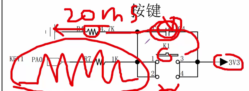
The input is the rising edge level
Capacitance is used to eliminate jitter (there is about 20ms jitter when pressing keys), which is used to eliminate jitter in hardware, and there is no need to eliminate jitter in software
1k resistor is a protective resistor to reduce the current and prevent pin breakdown
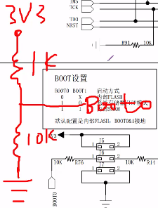
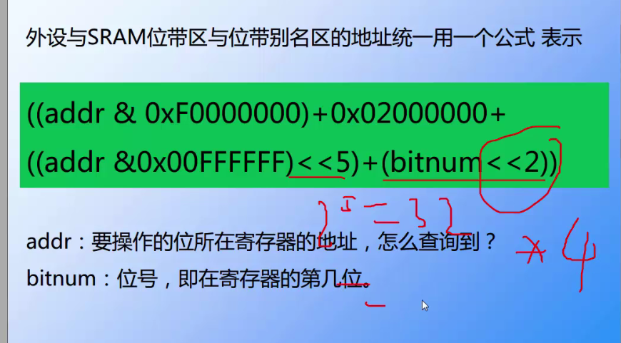
P14 bit band operation
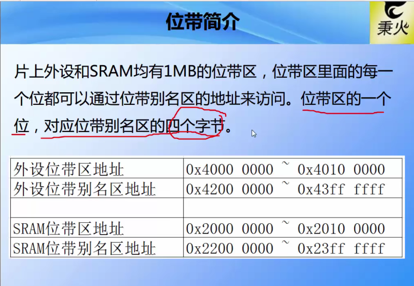
One address corresponds to one byte, and one byte has 8 bits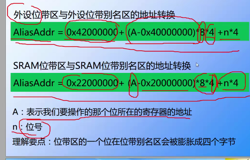
P15 explanation of startup documents
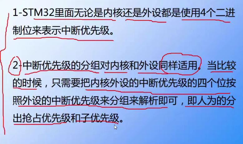
The smaller the interrupt priority value, the higher the priority
If the priority of the two software interrupts is the same, it depends on which hardware interrupt has the same priority
When writing an interrupt service function, the function name must be the same as that in the vector table
P16 RCC clock
You can check whether the SYSCLK system clock configuration is correct by reading the MCO clock output

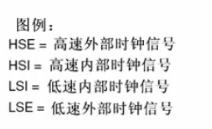
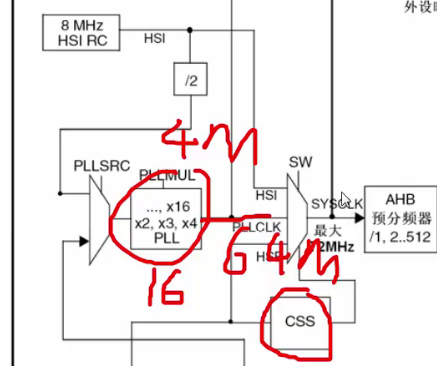
First, use HSE (8MHz) (high-speed external clock) to configure the system clock, go through PLLXTPRE without frequency division, then enter the PLL clock source to configure PLLSRC, and then enter the PLL frequency doubling factor to configure it to 9 times the frequency. It is concluded that the PLL clock PLLCLK is 72MHz. There are three choices when configuring the SYSCLK system clock: HSI/HSE/PLLCLK, Select that the PLL clock is equal to the system clock (72MHz).
Next, configure the frequency division factor of the three buses. The AHB high-speed bus is configured with 1 frequency division. The resulting AHB clock is 72MHz, and then enter the pre frequency division factor of APB1 and APB2. Since the maximum frequency of APB1 is 36MHz, select 2 frequency division. APB1 is the high-speed bus, and the maximum frequency is 72MHz, so it is configured as 1 frequency division. Then the bus has been configured. When using peripherals, configure the frequency division factor of peripherals.
Clock security system CSS
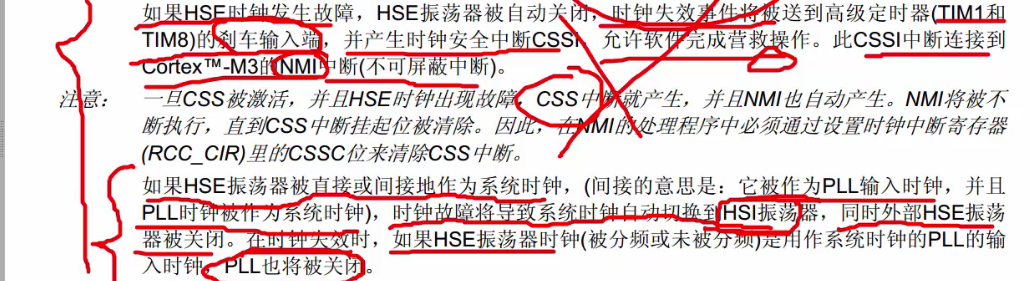
If the CSS interrupt is not enabled, the system will switch the clock to HSI in hardware, that is, 8MHz. Users need to select HSI to indirectly control PLL in software to generate 64MHz (8 / 2 * 16) clock. Some peripherals can still be used, but the safest thing is to alarm or inform users of failure.
P17 interrupt application summary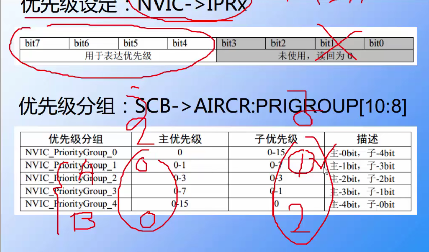
Compare the primary priority first, and then the sub priority. If it is the same, compare the hardware interrupt number (which can be found in the interrupt vector table) and the lower the higher the priority
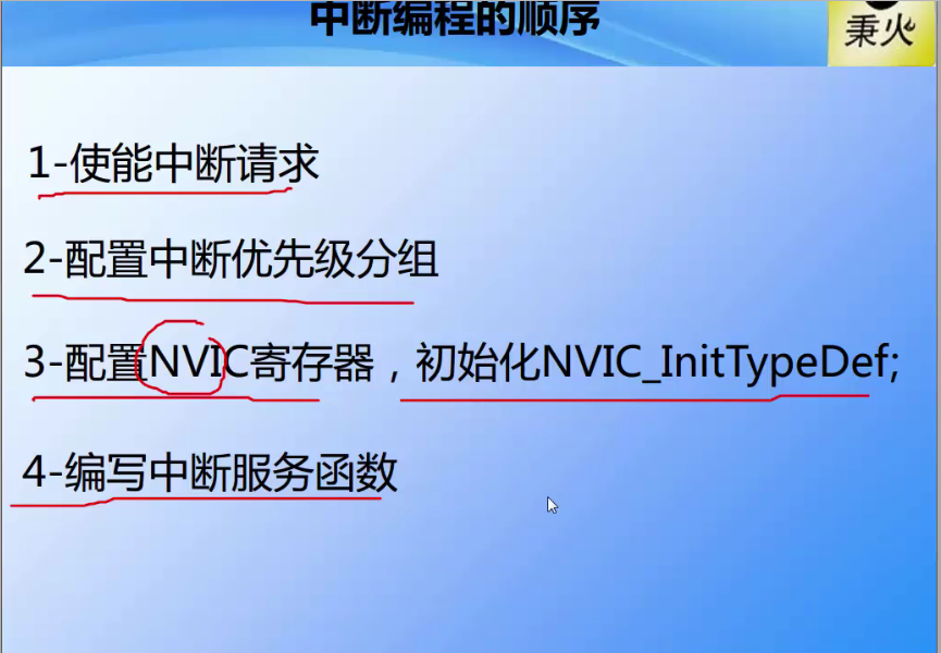
The interrupt enable in the NVIC is the main switch, and the interrupt enable of the peripheral is the small switch. The interrupt of the peripheral can be used only when the main switch and the switch of the peripheral are turned on.
The interrupt source is stm32f10x IRQN in H file_ Type structure
The name of the interrupt service function and the startup file startup_ stm32f10x_ hd. The name of the interrupt service function defined in the vector table in S is the same
Interrupt service functions are placed in stm32f10x_it.c, which is convenient for unified management and priority allocation
P18 EXTI (external interrupt / event controller)
GPIO must read a level to generate an interrupt. The level has a rising edge or a falling edge. These two signals generate an interrupt through EXTI and then give it to the kernel NVIC. That is, go to GPIO, EXTI and NVIC first.
The firmware library file of NVIC is in misc H medium
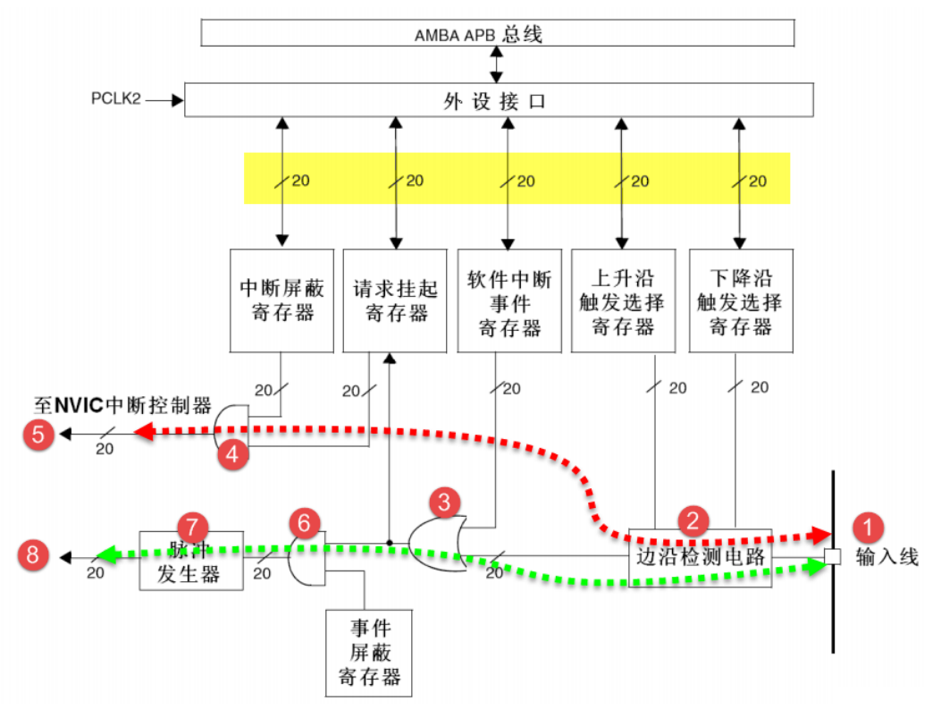
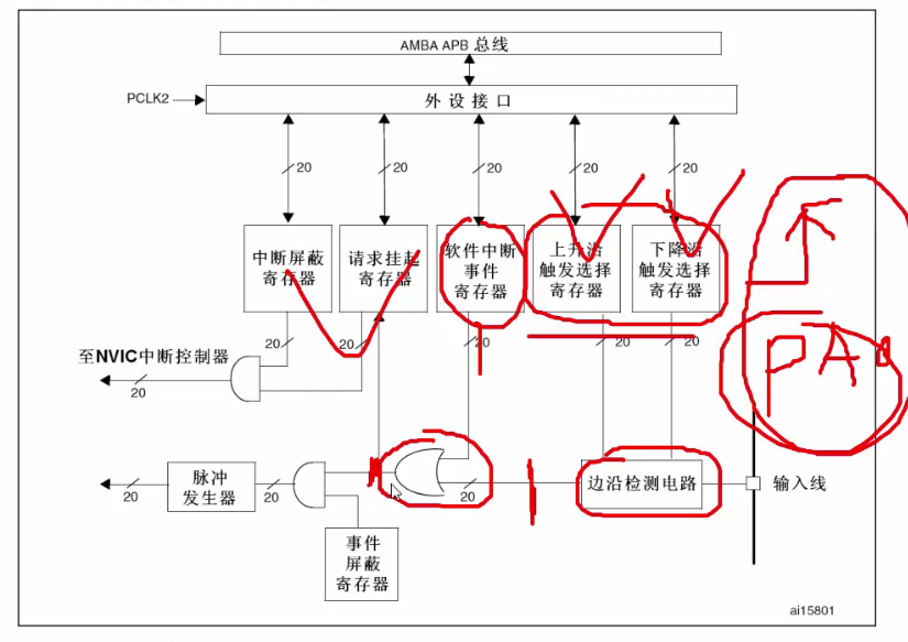
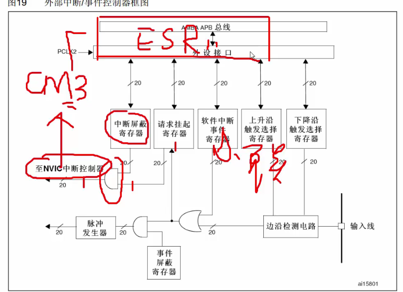
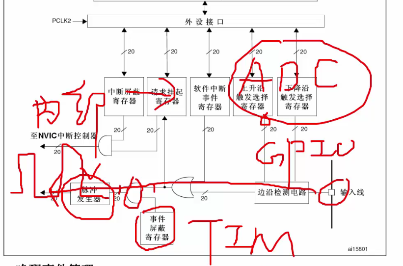 Trigger event: the pulse generator is inside the single chip microcomputer. After triggering, it generates a pulse signal, which can be used to control the ADC to start collecting or the timer to start counting and other events.
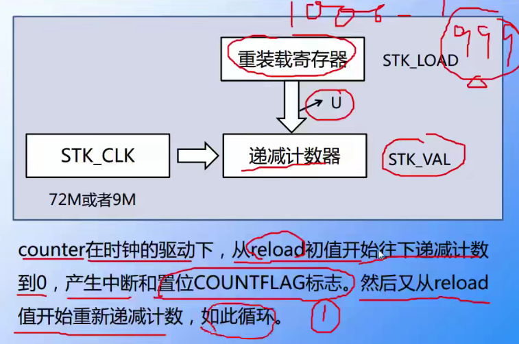
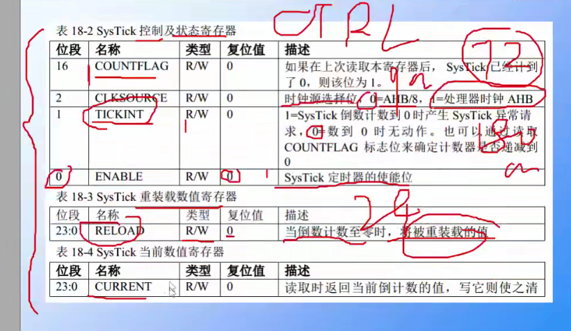
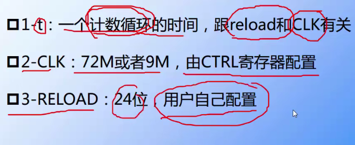
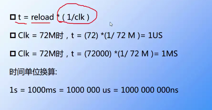
P19 SysTick system timer
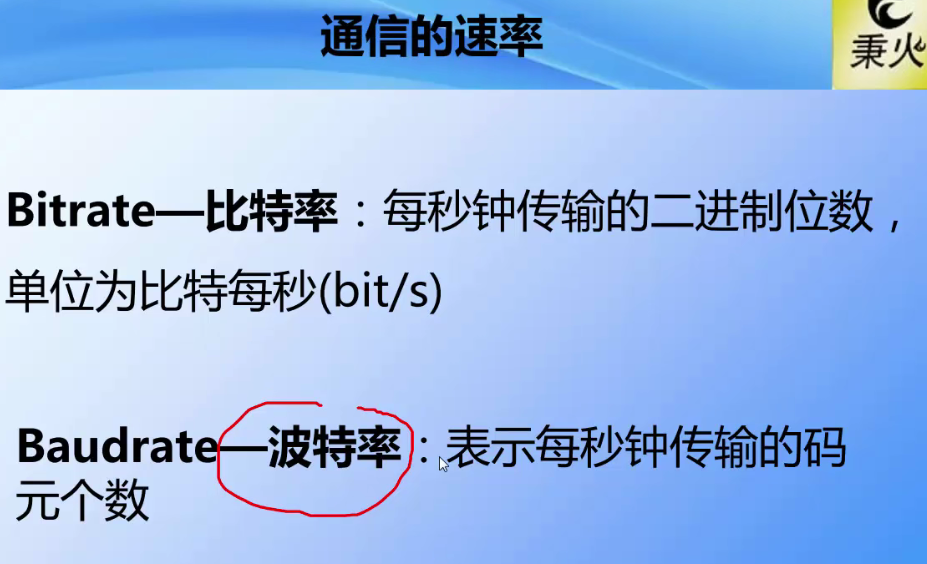
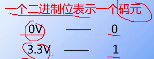
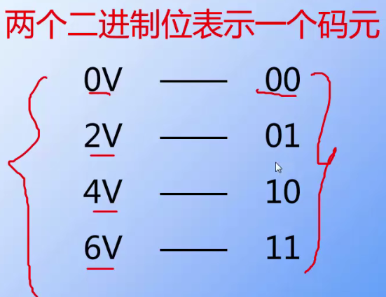
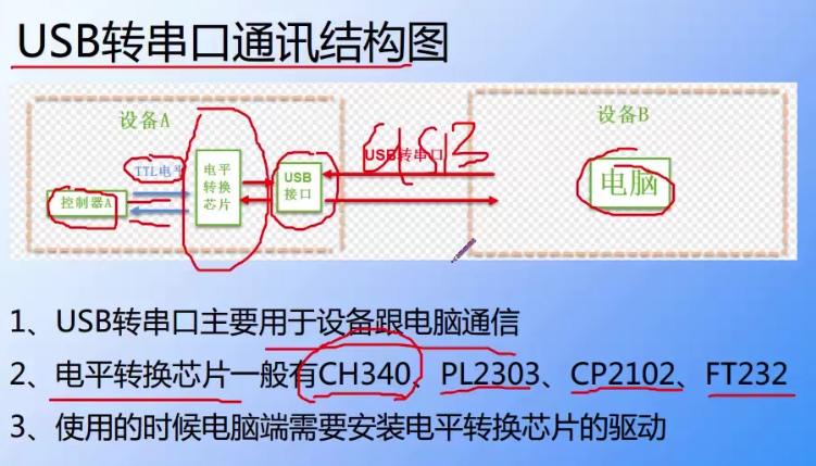
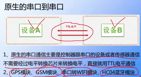
P20 basic concepts of communication
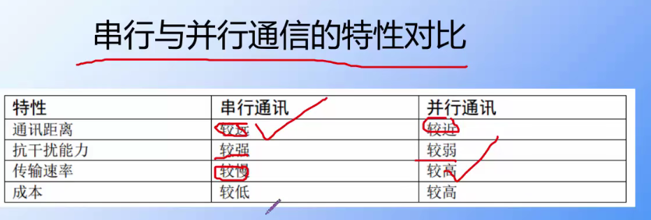
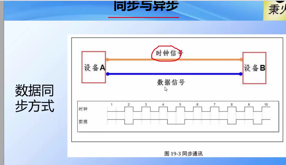
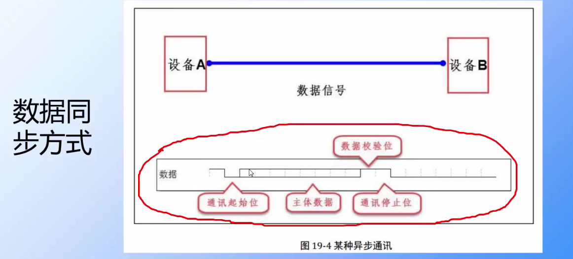
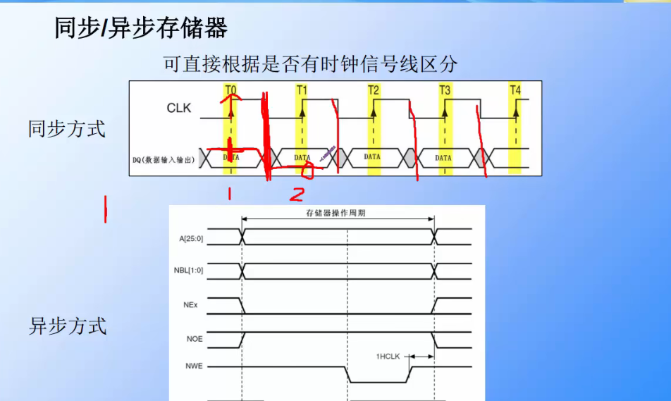
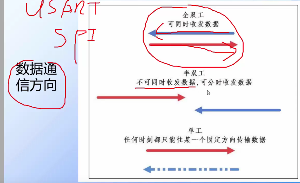 Synchronous and asynchronous: those with clock signal are called synchronous, and those without clock signal are called asynchronous
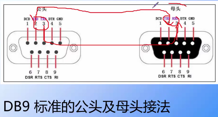
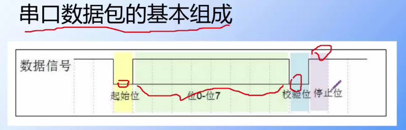
P21 serial communication
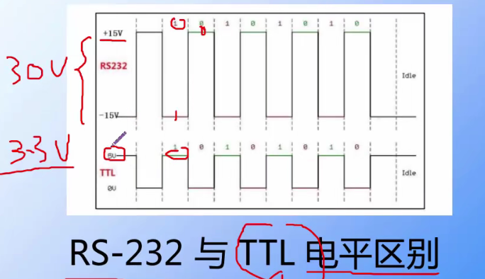
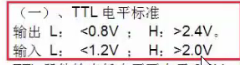
From the MCU or chip out of the TTL level
RS232: logic 1 is - 15V, logic 0 is + 15V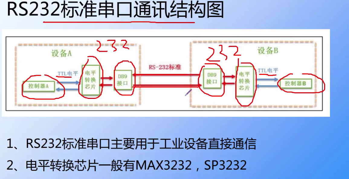
Explanation of stm32 serial port function block diagram
n indicates that the low level is valid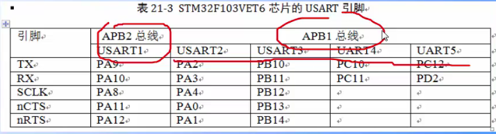
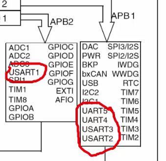
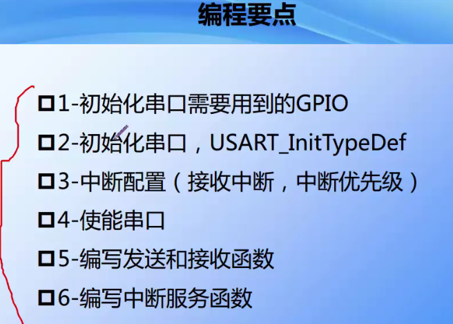
Note that serial port 1 is attached to APB2 bus and serial ports 2, 3, 4 and 5 are attached to APB1 bus. Pay attention to modifying the clock during programming
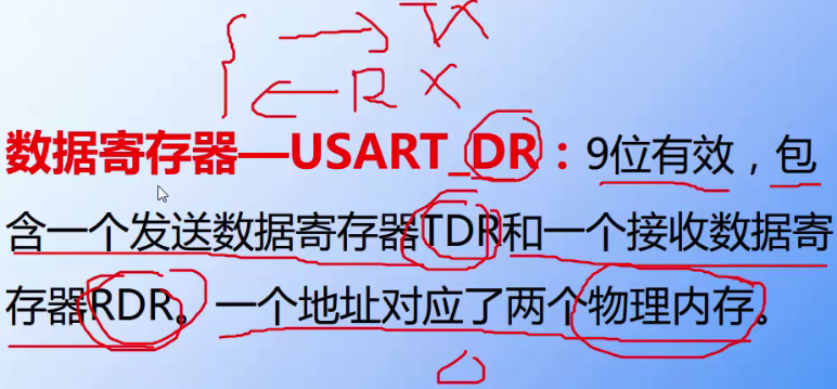
Serial port is full duplex communication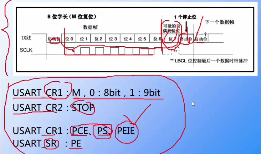

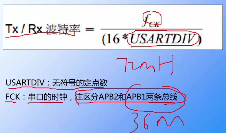 APB1 is a low-speed clock, 36M
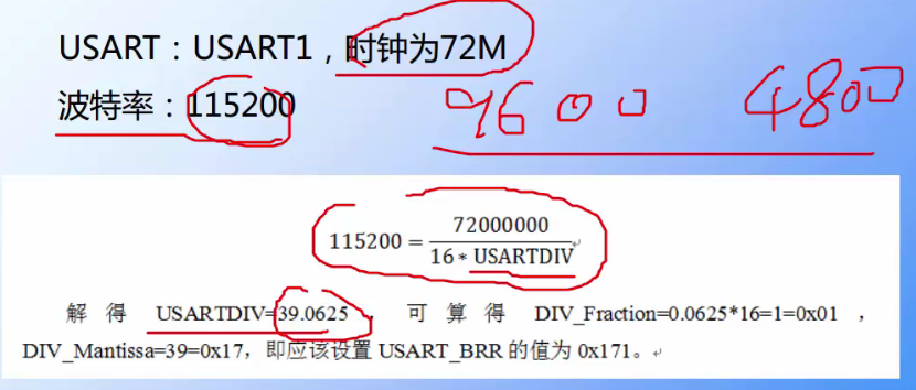
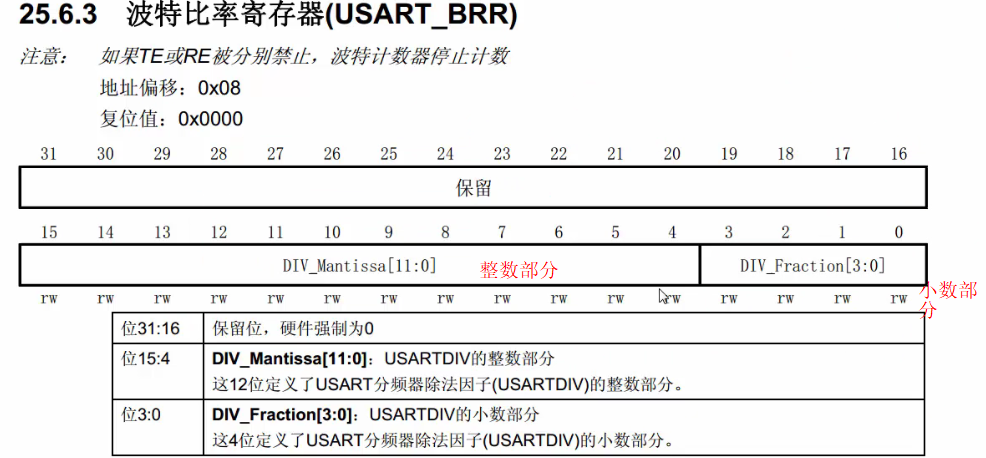
USART_BRR register is divided into integer part and decimal part. The decimal part is four digits and the minimum resolution is 1 / 16 = 0.065
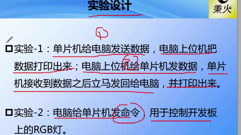
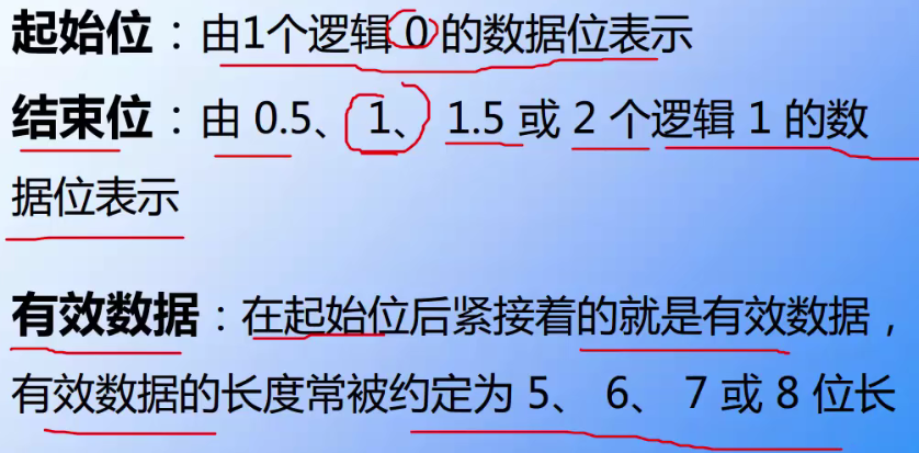
Serial port transmission is a byte by byte transmission, that is, 8-bit and 8-bit transmission
Multiple bytes or arrays or strings are sent with a circular statement
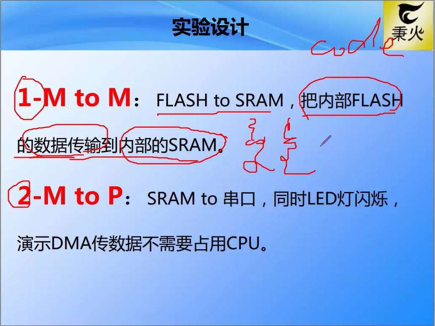
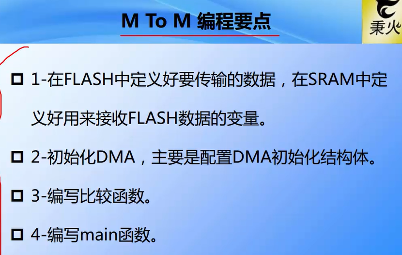
P22 DMA
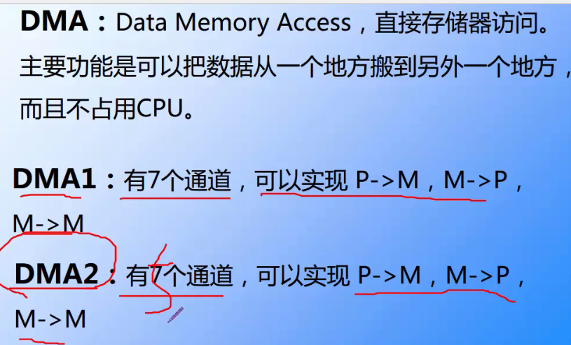
M refers to Memory, i.e. register, and P refers to Peripheral, i.e. Peripheral
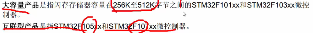
DMA2 only exists in high-capacity and interconnected products
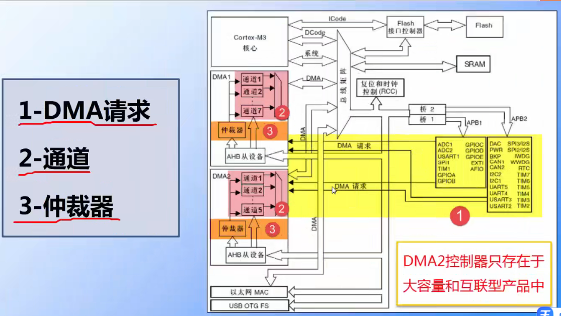
 Memory to Memory mode can access any channel of DMA1 and DMA2
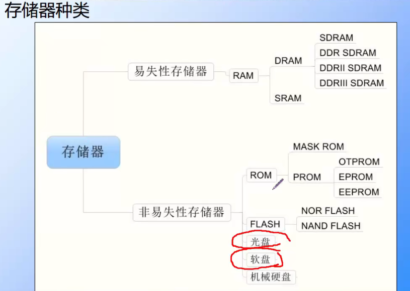
P23 memory
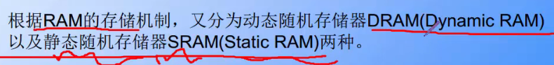
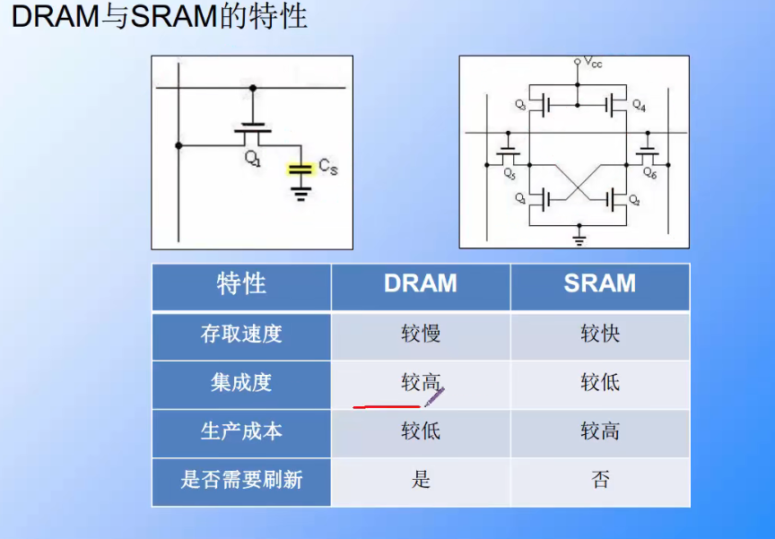
RAM (random access memory): data will be lost after power failure, but the reading and writing speed is fast
ROM (read only memory): data will not be lost after power failure, but the reading and writing speed is slow
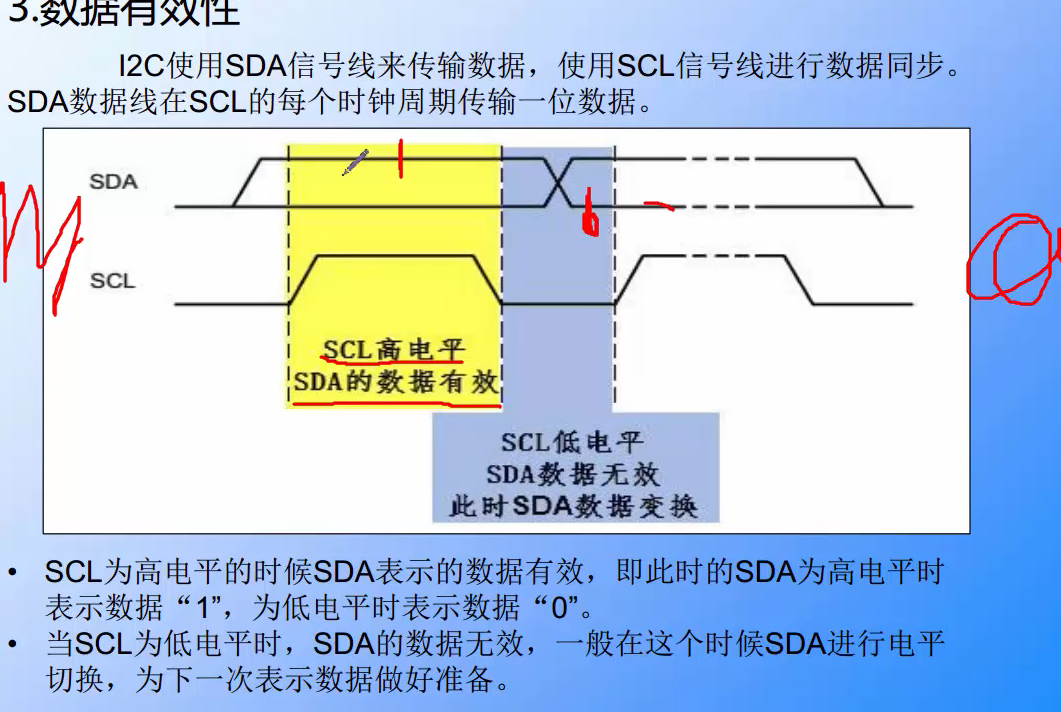
P24 I2C
24.1 physical layer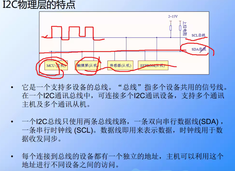
When the device is idle, the output high resistance state can prevent interference to other devices
When logic 1 is output, it is also in the high resistance state. If you want to, connect the host directly to the pull-up resistor and use the voltage of the pull-up resistor to generate a high level (as shown in the figure)
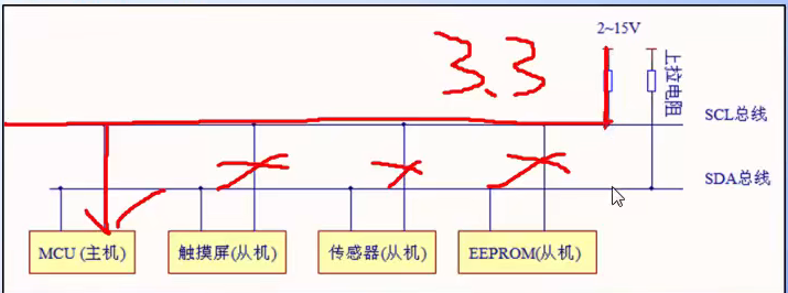
The slave pulls the bus to a low level by outputting a low level, indicating that the slave is occupying the bus, and other devices will not be used again.
Open drain output is not output voltage , control output Low level When the pin is grounded, the control output High level When the pin outputs neither high level nor low level, it is in high resistance state. If external Pull-up resistance , the voltage will be pulled to the power supply voltage of the pull-up resistor at the output high level. This method is suitable for connecting peripherals Voltage ratio When the voltage of single chip microcomputer is low.
24.2 protocol layer
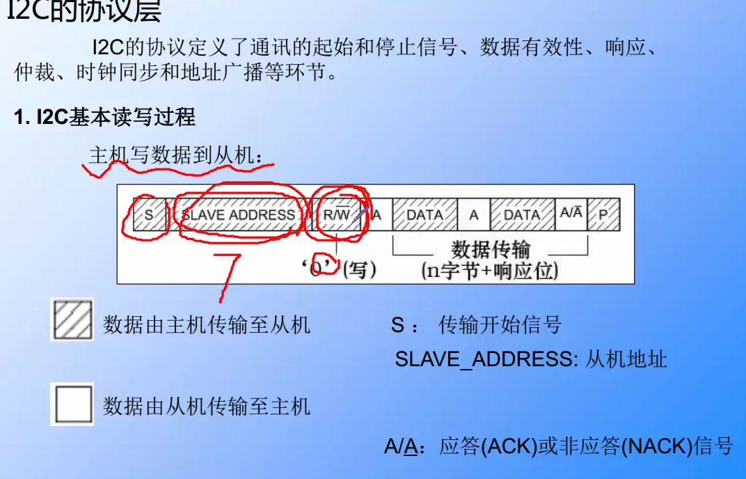
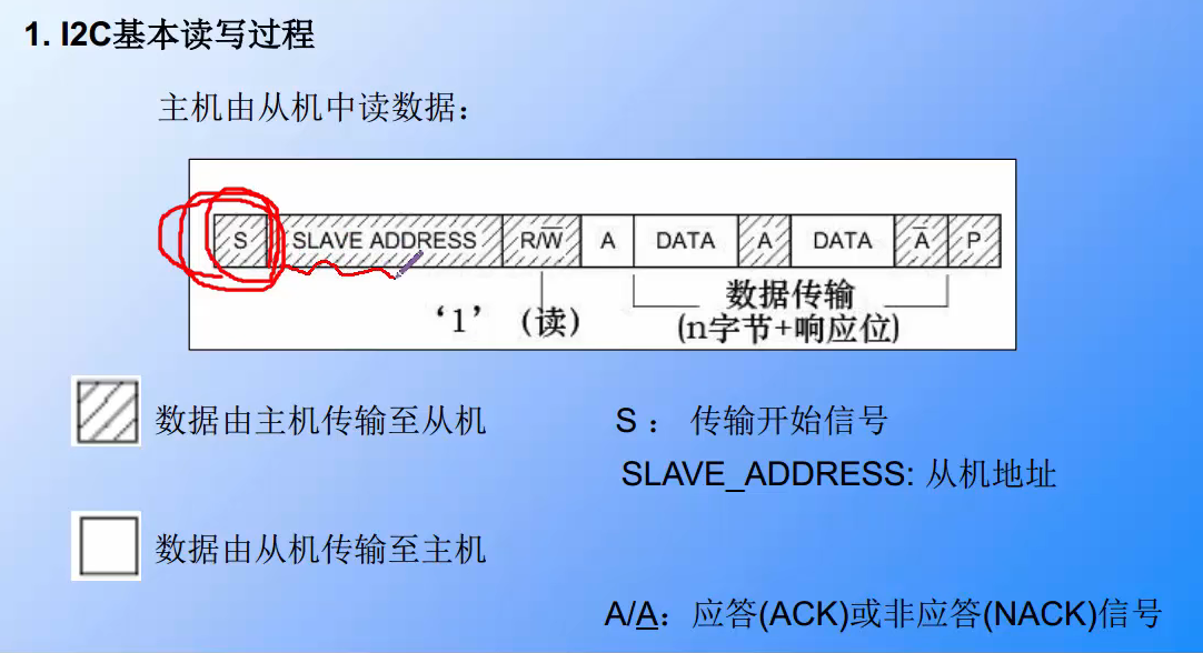
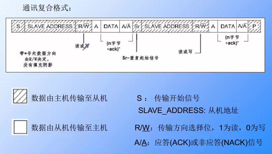
The communication composite format can read a bit in a register
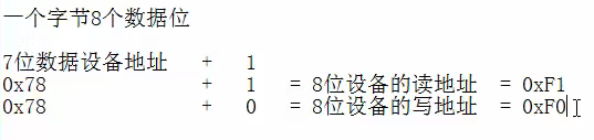
The 7-bit device address refers to the address of the slave, and the 8-bit device address refers to the slave address plus "read / write"
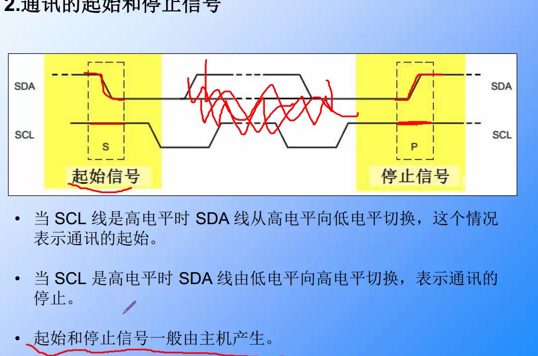
When the data transmission is released, the data transmission is stopped at the SDA control end. If the data transmission is at the SDA control end, the data transmission is stopped
PCLK1 refers to the clock of APB1
P25 SPI -- read / write serial FLASH
Even if only the data is read from the slave, the operation can only be performed when the host sends data to the slave, because the SCK clock will be turned on only when the host sends data
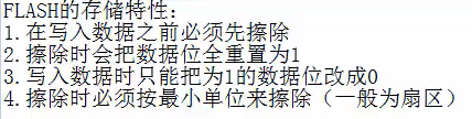
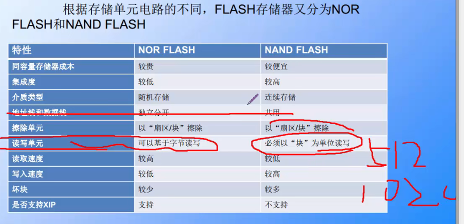
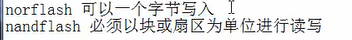
There is no size limit when writing norflash. You can write byte by byte without writing sector by sector
Or equal to "| =" is like adding, and equal to "& =" is equivalent to itself (but it can be used to take a byte of multiple bytes, such as 32-bit data 0xaabbccdd and 8-bit data 0xff for & operation to obtain the lowest 8-bit data, namely 0xdd)
To determine whether the data overflows (exceeding the maximum space of the stack), you can_ it. Hardfallut in C file_ Set a breakpoint at the handler function for debugging. If the program is stuck here, it indicates that it is indeed an error caused by overflow. The problem can be solved by defining the array outside the function, that is, as a global variable. The global variable uses not the stack space, but the free space of memory.