catalogue
-
- Which STM32 have CANFD peripherals
- Reference documents
- CAN-FD characteristics
- CAN-FD format
- CAN 2.0 VS CAN-FD
- STM32 FDCAN peripheral characteristics
- Bit time and sampling point
- Message RAM
- Filter settings
- Rx FIFO
- Rx Buffer VS Rx FIFO
- Tx Buffer, Tx FIFO, Tx Queue
- Operation mode
- Transceiver delay compensation TDC
- Clock calibration
- Low power mode
- Upgrade existing BxCAN to CANFD
- Use the next one
- WeChat official account
Which STM32 have CANFD peripherals
STM32G0, STM32G4, STM32H7, STM32L5,STM32MP1 series
Reference documents
- AN5348_ Application Manual of FDCAN peripheral on STM32 device: dm00625700-fdcan-peripheral-on-stm32-devices-stmicroelectronics.pdf
- STM32G4-FD-CAN
- AN5405_ FDCAN protocol used when loading programs for stm32h7 and STM32L5 series microcontrollers: dm00660346-fdcan-protocol-used-in-the-stm32-bootloader-stmicroelectronics.pdf
CAN-FD characteristics
The main functions of CAN-FD protocol are as follows:
- Compatible with CAN protocol, CAN-FD node can send / receive can messages according to ISO 11898-1 standard
- Error check improvement, up to 21 bit CRC check
- Message Priority
- Delay time guarantee
- Configuration flexibility
- Multicast reception with time synchronization
- System wide data consistency, with a maximum of 64 bytes per message
- multi-master
- Error detection and signaling
- The difference between temporary error and permanent error, node failure and automatic shutdown of defective nodes
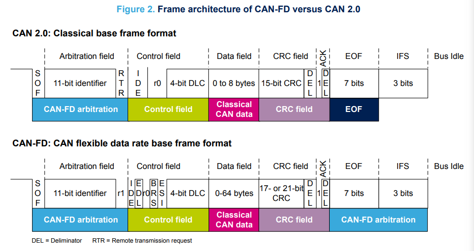
CAN-FD format
The data sent by CANFD is packaged into a message, which is divided into three segments:
- The first arbitration phase of the first arbitration segment is shown in the left blue part of the figure below
- Data segment data phase, the red part in the figure below
- The second arbitration phase, the blue part on the right in the figure below
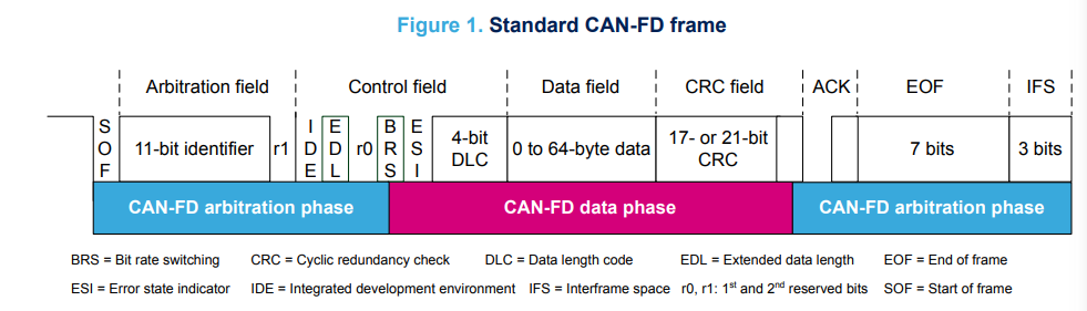
The above figure is only the CAN-FD format of the standard frame. The extended frame is added with an 18 Bit identifier after the IDE bit
First arbitration paragraph:
- 1-bit frame start SOF
- Arbitration field, arbitration domain, ID number and other bits, indicating the purpose of the message (providing or requesting data) and speed and format configuration (CAN or CAN-FD). The standard frame is 12 bit = 11 bit ID + 1-bit R1, and the extended frame is 32 bit = 11 bit base ID + 1-bit R1 + 1-bit ide + 18 Bit extended ID + 1-bit R0, where the IDE should be identifier extension, This bit is used to distinguish between standard frames and extended frames
The split point of arbitration segment and data segment is in BRS bit, BRS: Bit rate switching, which is used to indicate whether to change the rate, such as switching from 500K to 2M, or keeping 500K unchanged
Data segment:
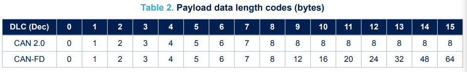
- The data length code (DLC) indicates the number of data bytes contained in the message. There are only 4 bits, 16 types in total, so there can only be 16 fixed bytes [0,8], 12, 16, 20, 24, 32, 48 and 64
- Data the user wants to send
- Cyclic redundancy sequence check (CRC) ensures the integrity of data transmission in the following ways: level 17 polynomial is used to CRC the payload within 16 bytes, and level 21 polynomial is used to verify the payload between 16 bytes and 64 bytes
- Dominant position
The second arbitration paragraph:
- Acknowledgement receiver (ACK) sent by other nodes on the bus (if at least one has successfully received the message)
- End of frame (EOF), no message is sent during IFS to separate the current frame from the next frame
Bring in some other CAN-FD diagrams to further understand:
In the following figure, RRs = remote request substitution in CAN, RRS is not used in CAN-fd, SRR = substitute remote request, IDE = identifier extension, FDF = flexible data rate format, d = dominant, r = recursive, R0 = reserved: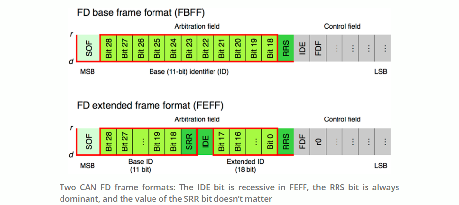
In the figure below, IDE (identifier extension), FDF (flexible data rate format), BRS (bit rate switch; acceptable, if alternate bit rate), ESI (error state indicator; acceptable, if error passive):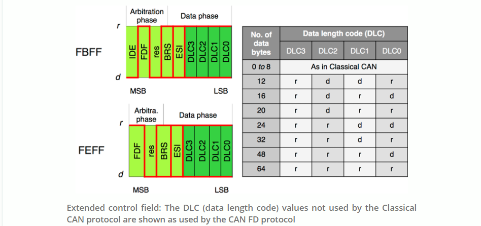
Two variants of FDCAN:
- Long Frame Mode (LFM) is a long frame mode with constant rate, and the length is increased from 8 bytes to 64 bytes
- Fast Frame Mode (FFM) fast frame mode, control domain, data domain and CRC domain are transmitted at a higher rate, STM32 is up to 8Mbit/s, and BRS bit is set
Long frame mode and fast frame mode are generally used together
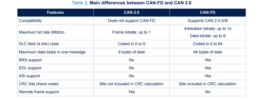
CAN 2.0 VS CAN-FD
Take the standard frame as an example:
RTR = Remote transmission request:
- In CAN 2.0, RTR is dominant (logic 0), indicating data frame, and recessive (logic 1), indicating remote frame
- CANFD only supports data frames, and RTR is always an explicit data frame, which can be understood as reserved
The IDE bit remains unchanged to distinguish between standard frames and extended frames
CANFD adds 3 bits to the control field:
- EDL, Extend data length, extended data length bit, recessive (logic 1) represents CANFD frame, and explicit (logic 0, R0) represents CAN2.0 frame
- BRS, Bit rate switching, bit rate switching, indicating whether to switch high-speed transmission, such as switching from 500K to 2M
- ESI, Error state indicator, indicates whether the node is in error active mode or error passive mode
DLC, Data Length Code, data length code, CAN 2.0 and CANFD are in the same position and the same 4-bit length, but the values after 8 have different meanings:
The CANFD payload is increased from the maximum 8 bytes of CAN 2.0 to the maximum 64 bytes, which improves the network bandwidth and reduces the demand for multi packet processing. Therefore, the message integrity is enhanced by adding more bits to the CRC field:
- The payload is 16 bytes or less, and the CRC is encoded in 17 bit
- The payload is 20 bytes or more, and the CRC is encoded in 21 bit
In addition, in order to ensure the robustness of CAN-FD frame, the filling bit mechanism supports CRC field
Can refer to CAN bus six BOSCH CAN bit filling (coding rules), zeroing coding (RZ) and non zeroing coding (NRZ) , bit filling is used after five consecutive bits of the same polarity. Six consecutive bits of the same polarity are considered errors. A side effect of the bit filling scheme is that a small number of bit errors in the received message may destroy the de filling process (the receiver needs to remove the filling bits), resulting in a large number of errors propagating in the de filling message. This reduces the level of protection provided by CRC against original errors. The shortcomings of the protocol have been solved in the CAN FD frame by using a combination of fixed padding bits and a counter recording the number of padding bits inserted.
The following figure gives a comparative summary, mainly the increase of data payload and the higher speed ensured by BRS, EDL and ESI bits available in CAN-FD:
STM32 FDCAN peripheral characteristics
characteristic:
- Parts A and B according to CAN 2.0 and ISO 11898-1:2015, - 4
- The accessible 10 KB RAM memory is 32-bit, 1 word = 4 bytes, and up to 2560 words CAN be allocated, which is shared by all CAN peripherals
- Improved receive filtering
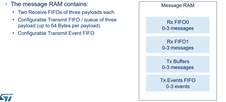
- Two configurable receive FIFO s
- Up to 64 dedicated receive buffers
- Separate signaling when receiving high priority messages
- Up to 32 dedicated send buffers
- Configurable transmit FIFO and transmit queue
- Configurable send event FIFO
- Clock calibration unit
- Transceiver delay compensation
A FDCAN peripheral block diagram:
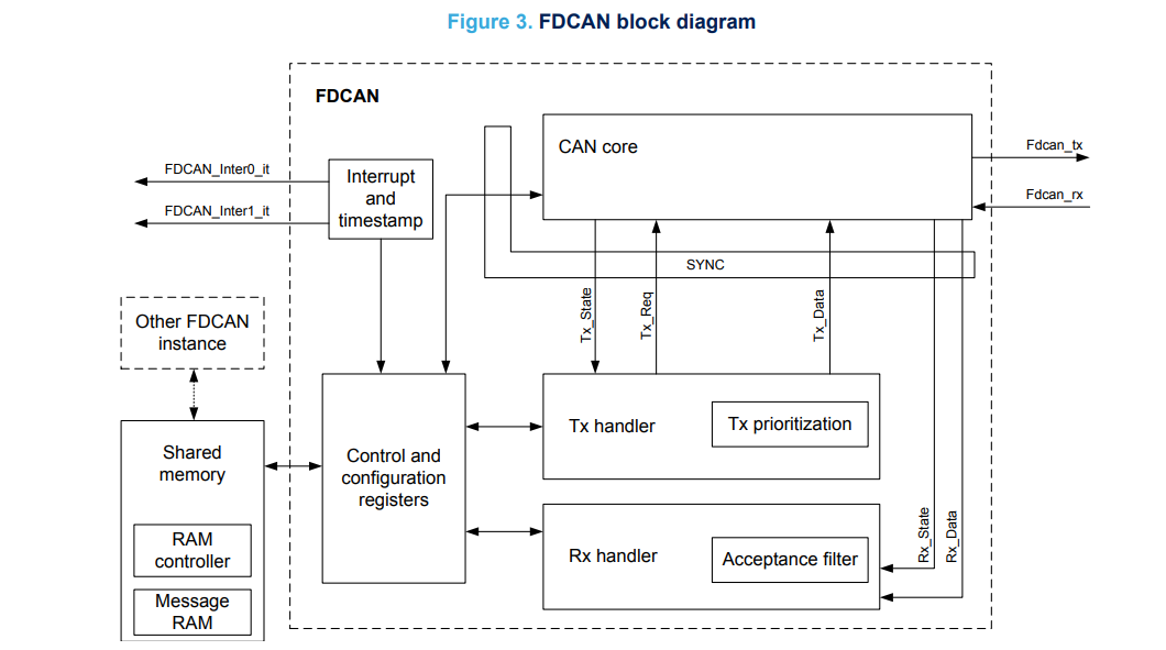
Note that Shared Memory is shared by all FDCAN peripherals
3-way FDCAN block diagram of STM32G4:
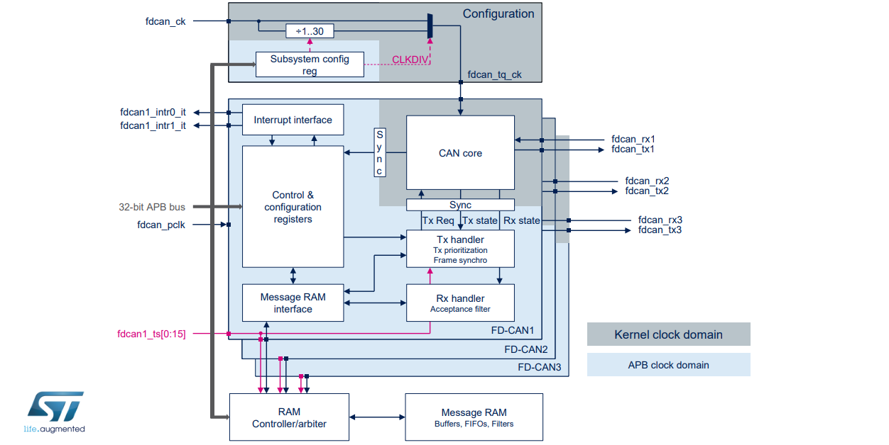
The arbitration segment bit rate is up to 1Mbit/s, and the data segment bit rate is up to 8Mbit/s
support:
- 2 maskable interrupts per controller
- power-down
- CAN error logging
- AUTOSAR and J1939
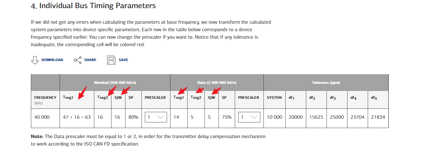
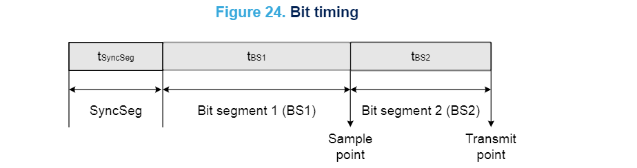
Bit time and sampling point
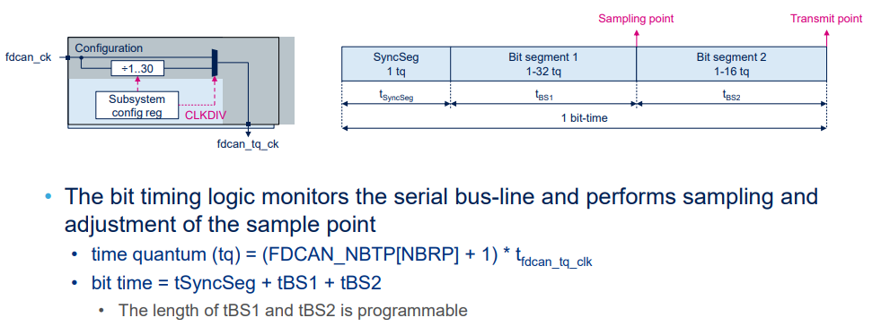
The sampling points of all nodes in the same network shall be consistent, generally 75% ~ 80%. Otherwise, when sending, the bus will enter error passive state or bus off
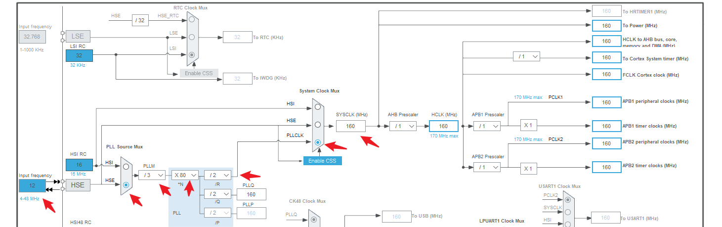
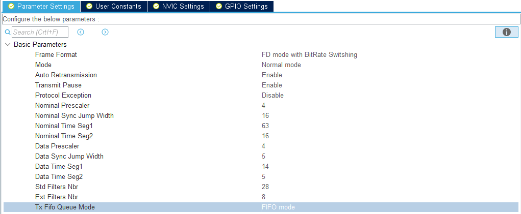
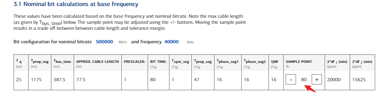
Generally, the master clock is set to 40MHz (which can be realized after frequency division), and then other parameters are set, such as STM32G4:
FDCAN in 500K@2M Configuration when:
Calculation formula reference:
    /*
     * Bit timing & sampling
     * Tq = (BRP+1)/Fcan if DIV8 = 0
     * Tq = 8*(BRP+1)/Fcan if DIV8 = 1
     * TSync = 1.Tq
     * TSeg1 = (TSEG1+1)*Tq                >= 3Tq
     * TSeg2 = (TSEG2+1)*Tq                >= 2Tq
     * Bit Time = TSync + TSeg1 + TSeg2    >= 8Tq
     *
     * Resynchronization:
     *
     * Tsjw = (SJW + 1)*Tq
     * TSeg1 >= Tsjw + Tprop
     * TSeg2 >= Tsjw
     */
123456789101112131415
Arbitration section:
- Clock = 160M / Nominal Prescaler = 160M / 4 = 40MHz
- 1 CAN bit = (1 + Tseg1 + Tseg2) TQ = 80 TQ (time quanta)
- Communication rate = 40M / (1 + Tseg1 + Tseg2) = 40M / (63 + 16 + 1) = 500Kbit/s
- Sampling point = (1 + Tseg1) / ((1 + Tseg1 + Tseg2)) = 64 / 80 = 0.8
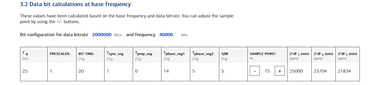
Data segment:
- Clock = 160M / Data Prescaler = 160M / 4 = 40MHz
- 1 CAN bit = (1 + DTseg1 + DTseg2) TQ = 20 TQ (time quanta)
- Communication rate = 40M / (1 + DTseg1 + DTseg2) = 40M / (14 + 5 + 1) = 2Mbit/s
- Sampling point = (1 + DTseg1) / ((1 + DTseg1 + DTseg2)) = 15 / 20 = 0.75
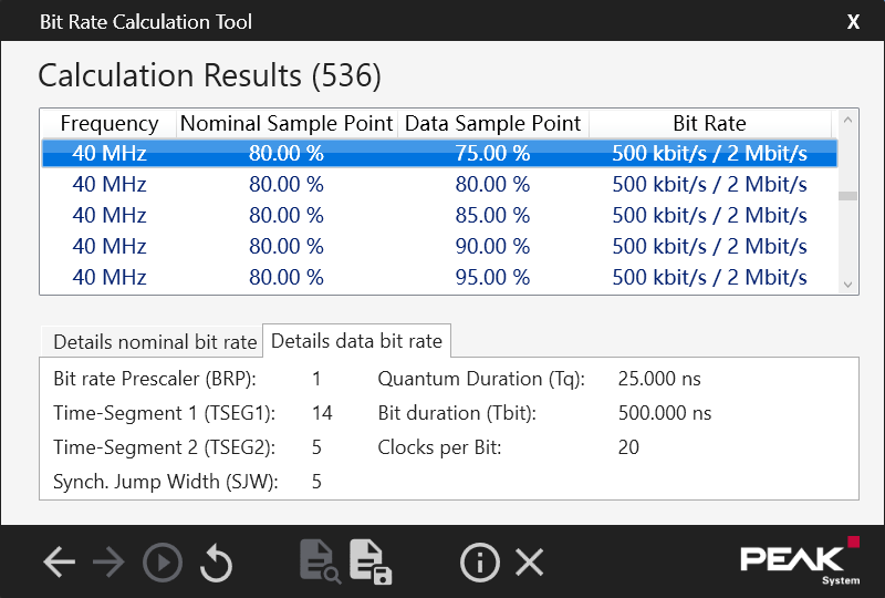
Can pass KVASER Bit Timing Calculator for CANFD This website calculates online
The clock source is 40M by default and does not change:
Bit rate setting 500K@2M :
The sampling point of arbitration section is changed to 80%:
The sampling point of the data segment is changed to 75%:
Finally, calculate the values of tseg1, tseg2 and SJW:
Bit Rate Calculation Tool for PEAK It's also very good to use
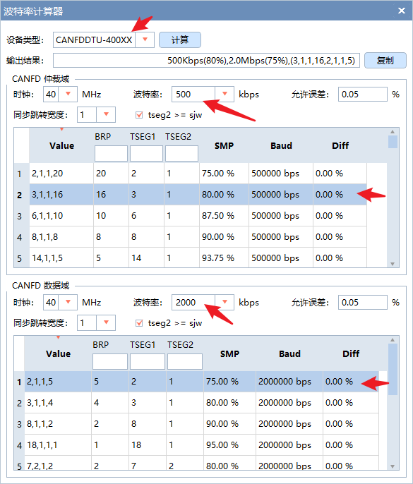
Of course, there are more than these configurations. baudcal.exe in Zhou Ligong's ZCANPRO software installation directory can also be counted as:
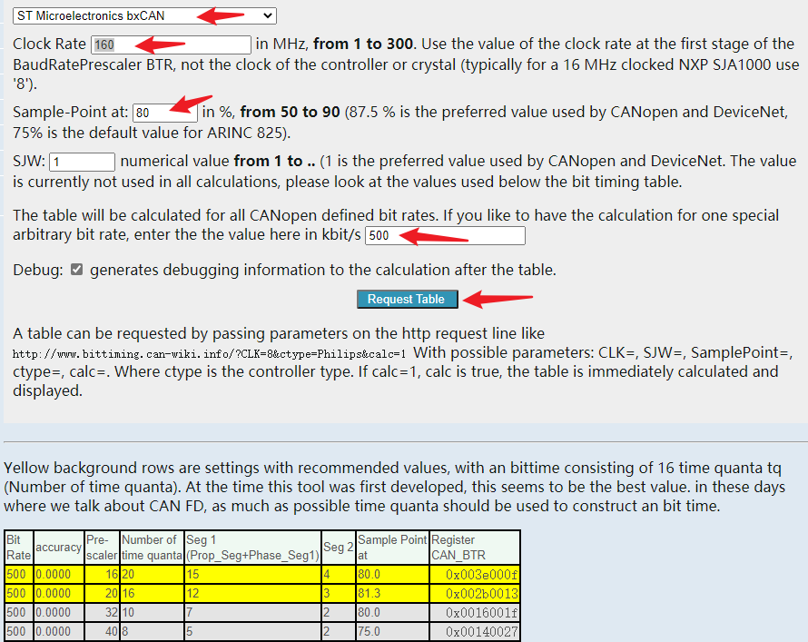
The calculation of stm32 arbitration segment can refer to this website CAN Bit Time Calaulation:
Or reference S32K series learning notes -- FlexCAN module introduction and routine establishment , follow some algorithms to calculate by yourself:
CAN The baud rate cycle is divided into 12-20 Time period
 The sampling point is usually selected at 75% of the baud rate cycle%-80% paragraph
 Remaining 20%-25% Will act Phase_Seg2 Value of
Phase_Seg1 The value of is the same as Phase_Seg2 The values are the same
Sync_Seg Is a time period
Resync Jumo Width(RJW+1)= Phase_Seg2(If Phase_Seg2<4,(RJW+1)=4)
123456
Message RAM
All sent and received messages are stored in the CAN message RAM. During the initialization of the CAN message RAM, the user must define the 11 bit filter, the 29 bit filter, the storage location of the received messages and the messages to be transmitted
The CAN message RAM is divided into four different parts:
- Filtering (11 bit filter, 29 bit filter)
- Receive (Rx FIFO 0, Rx FIFO 1, Rx Buffer)
- Send (Tx event FIFO, Tx Buffer)
- Trigger Memory
As shown in the figure below:
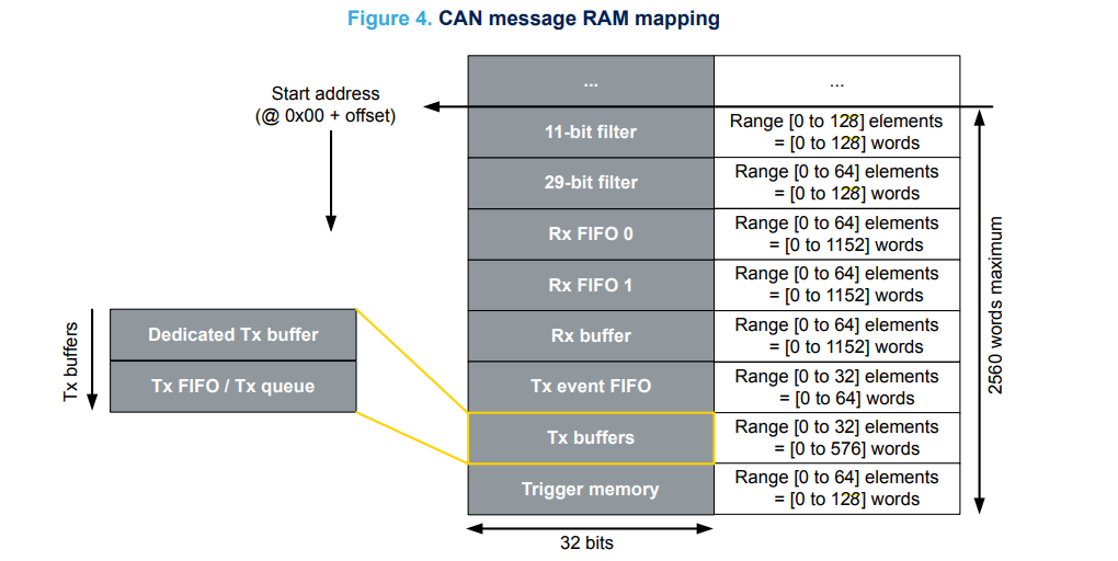
At first glance, it's not good, but this is only the maximum allocation of 10KB RAM for one CANFD. If multiple CANFD peripherals, such as the three-way CANFD of STM32G4, are used together, the resources allocated to each way will be poor
All parts of FDCAN peripherals CAN be configured by the user. The sum of all elements of all parts shall not exceed the total size of CAN message RAM. The RAM provides higher flexibility and performance by eliminating redundant parts and expanding enough memory for other parts.
Allocate the configured elements of each part in the CAN message RAM in a dynamic and continuous manner according to the sequence shown in the above figure; However, in order to avoid the risk of exceeding RAM and for reliability reasons, each segment is not assigned its own start and end addresses.
For the so-called dynamic allocation, it's very painstaking to dig out some points from 10KB memory for other peripherals. It's easy to bury a hole if you have to allocate it by yourself
Receiving and sending messages means storing "elements" at the ram level. This "element" contains only identifier, DLC, control bits (ESI, XTD, RTR, BRS, FDF), data fields and specific transmit / receive bit fields for control. The remaining bits of the CAN message are automatically processed by the hardware and will not be saved in RAM.
The specific bit fields used to control reception are filter index, accepted mismatched frames and Rx timestamp.
The specific bit fields used for transmission are message marker and event FIFO control bits
The number of word s allocated to each element of Tx buffer, Tx FIFO, Tx queue or Rx buffer is calculated as follows:
- Header information (two reserved 32-bit-words, equivalent to 8 bytes) to allocate identifier, DLC field, control bit and specific send / receive bit field
- Data (enough 32-bit-words) contains the number of bytes per data field
The calculation formula is: element size (in words) = header information (2 words) + Data (Data field / 4). When the Data field is 0 ~ 8, the Data takes 2 words, as shown in the following table:
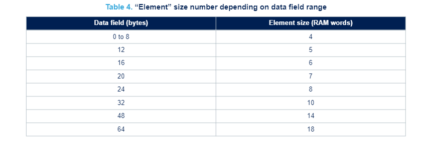
It is often said that the MTU should be this thing. For example, the Ethernet MTU value is set to 1500, the MTU of CAN2.0 is 16, and the MTU of CANFD is 72. The maximum 72 bytes of CANFD = > 18 words = > 1 T / R elements. At this time, the effective utilization rate is 64 / 72 = 88.88%
element is summarized as follows:
- 11 bit filter is a standard frame filter. Because the filter ID is set to 0~0x7FF, there are two filters in total. Generally, the one in mask mode is set to CAN_ID, one set as mask, occupying 2 * 2 = 4 bytes, 1 standard frame filter element = 4 bytes = 1 word
- 29 bit filter, extended frame filter, because the filter ID is set to 0 ~ 0x1ffffff, there are two in total, usually one is set to can in mask mode_ ID, one set as mask, occupying 2 * 4 = 8 bytes, 1 extended frame filter element = 8 bytes = 2 words
- Sending and receiving not only need to receive valid data (up to 64 bytes), but also include things in the data link layer (BRS, etc.). It is possible to receive standard CAN, CANFD, standard frame and extended frame. According to the maximum, the CANFD MTU is fixed at 72, so 1 Rx element = 72 bytes = 18 words, 64 * 18 = 1152
The following figure is an example of 10KB RAM allocated to 2-way FDCAN:
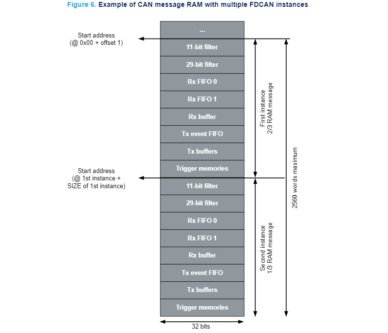
We can see that distribution is still very free
If you really hate these things, you can just ignore them. The initialization part of the code generated by stm32pubemx will automatically call the function of allocating RAM, and intercept the relevant code automatically generated by STM32G474 using the 3-channel CANFD part, as follows:
#define PERIPH_BASE           (0x40000000UL) /*!< Peripheral base address */
#define APB1PERIPH_BASE        PERIPH_BASE
#define SRAMCAN_BASE          (APB1PERIPH_BASE + 0xA400UL)

#define SRAMCAN_FLS_NBR                  (28U)         /* Max. Filter List Standard Number      */
#define SRAMCAN_FLE_NBR                  ( 8U)         /* Max. Filter List Extended Number      */
#define SRAMCAN_RF0_NBR                  ( 3U)         /* RX FIFO 0 Elements Number             */
#define SRAMCAN_RF1_NBR                  ( 3U)         /* RX FIFO 1 Elements Number             */
#define SRAMCAN_TEF_NBR                  ( 3U)         /* TX Event FIFO Elements Number         */
#define SRAMCAN_TFQ_NBR                  ( 3U)         /* TX FIFO/Queue Elements Number         */

#define SRAMCAN_FLS_SIZE            ( 1U * 4U)         /* Filter Standard Element Size in bytes */
#define SRAMCAN_FLE_SIZE            ( 2U * 4U)         /* Filter Extended Element Size in bytes */
#define SRAMCAN_RF0_SIZE            (18U * 4U)         /* RX FIFO 0 Elements Size in bytes      */
#define SRAMCAN_RF1_SIZE            (18U * 4U)         /* RX FIFO 1 Elements Size in bytes      */
#define SRAMCAN_TEF_SIZE            ( 2U * 4U)         /* TX Event FIFO Elements Size in bytes  */
#define SRAMCAN_TFQ_SIZE            (18U * 4U)         /* TX FIFO/Queue Elements Size in bytes  */

#define SRAMCAN_FLSSA ((uint32_t)0)                                                      /* Filter List Standard Start
                                                                                            Address                  */
#define SRAMCAN_FLESA ((uint32_t)(SRAMCAN_FLSSA + (SRAMCAN_FLS_NBR * SRAMCAN_FLS_SIZE))) /* Filter List Extended Start
                                                                                            Address                  */
#define SRAMCAN_RF0SA ((uint32_t)(SRAMCAN_FLESA + (SRAMCAN_FLE_NBR * SRAMCAN_FLE_SIZE))) /* Rx FIFO 0 Start Address  */
#define SRAMCAN_RF1SA ((uint32_t)(SRAMCAN_RF0SA + (SRAMCAN_RF0_NBR * SRAMCAN_RF0_SIZE))) /* Rx FIFO 1 Start Address  */
#define SRAMCAN_TEFSA ((uint32_t)(SRAMCAN_RF1SA + (SRAMCAN_RF1_NBR * SRAMCAN_RF1_SIZE))) /* Tx Event FIFO Start
                                                                                            Address */
#define SRAMCAN_TFQSA ((uint32_t)(SRAMCAN_TEFSA + (SRAMCAN_TEF_NBR * SRAMCAN_TEF_SIZE))) /* Tx FIFO/Queue Start
                                                                                            Address                  */
#define SRAMCAN_SIZE  ((uint32_t)(SRAMCAN_TFQSA + (SRAMCAN_TFQ_NBR * SRAMCAN_TFQ_SIZE))) /* Message RAM size         */

/**
  * @brief  Calculate each RAM block start address and size
  * @param  hfdcan pointer to an FDCAN_HandleTypeDef structure that contains
  *         the configuration information for the specified FDCAN.
  * @retval none
 */
static void FDCAN_CalcultateRamBlockAddresses(FDCAN_HandleTypeDef *hfdcan)
{
  uint32_t RAMcounter;
  uint32_t SramCanInstanceBase = SRAMCAN_BASE;
#if defined(FDCAN2)

  if (hfdcan->Instance == FDCAN2)
  {
    SramCanInstanceBase += SRAMCAN_SIZE;
  }
#endif /* FDCAN2 */
#if defined(FDCAN3)
  if (hfdcan->Instance == FDCAN3)
  {
    SramCanInstanceBase += SRAMCAN_SIZE * 2U;
  }
#endif /* FDCAN3 */

  /* Standard filter list start address */
  hfdcan->msgRam.StandardFilterSA = SramCanInstanceBase + SRAMCAN_FLSSA;

  /* Standard filter elements number */
  MODIFY_REG(hfdcan->Instance->RXGFC, FDCAN_RXGFC_LSS, (hfdcan->Init.StdFiltersNbr << FDCAN_RXGFC_LSS_Pos));

  /* Extended filter list start address */
  hfdcan->msgRam.ExtendedFilterSA = SramCanInstanceBase + SRAMCAN_FLESA;

  /* Extended filter elements number */
  MODIFY_REG(hfdcan->Instance->RXGFC, FDCAN_RXGFC_LSE, (hfdcan->Init.ExtFiltersNbr << FDCAN_RXGFC_LSE_Pos));

  /* Rx FIFO 0 start address */
  hfdcan->msgRam.RxFIFO0SA = SramCanInstanceBase + SRAMCAN_RF0SA;

  /* Rx FIFO 1 start address */
  hfdcan->msgRam.RxFIFO1SA = SramCanInstanceBase + SRAMCAN_RF1SA;

  /* Tx event FIFO start address */
  hfdcan->msgRam.TxEventFIFOSA = SramCanInstanceBase + SRAMCAN_TEFSA;

  /* Tx FIFO/queue start address */
  hfdcan->msgRam.TxFIFOQSA = SramCanInstanceBase + SRAMCAN_TFQSA;

  /* Flush the allocated Message RAM area */
  for (RAMcounter = SramCanInstanceBase; RAMcounter < (SramCanInstanceBase + SRAMCAN_SIZE); RAMcounter += 4U)
  {
    *(uint32_t *)(RAMcounter) = 0x00000000U;
  }
}

HAL_StatusTypeDef HAL_FDCAN_Init(FDCAN_HandleTypeDef *hfdcan)
  ...
  FDCAN_CalcultateRamBlockAddresses(hfdcan);
  ...
}
123456789101112131415161718192021222324252627282930313233343536373839404142434445464748495051525354555657585960616263646566676869707172737475767778798081828384858687888990
Convert (please correct if there is any error):
//The base address of the 11 bit filter is relatively offset. One CANFD channel is defined above, with a maximum of 28 standard frame filters
SRAMCAN_FLSSA = 0;
//The base address of the 29 bit fliter is relatively offset. One CANFD channel is defined above, with a maximum of 8 extended frame filters
SRAMCAN_FLESA = SRAMCAN_FLSSA + (SRAMCAN_FLS_NBR * SRAMCAN_FLS_SIZE) = 0 + 28 * 4 = 112;
//The base address of Rx FIFO 0 is relatively offset, and the depth of Rx FIFO 0 is 3. At most 3 CANFD frames can be thrown in. Poor, weak and helpless
SRAMCAN_RF0SA = SRAMCAN_FLESA + (SRAMCAN_FLE_NBR * SRAMCAN_FLE_SIZE) = 112 + 8 * 2 * 4 = 176;
//The base address of Rx FIFO 1 is relatively offset, and the depth of Rx FIFO 1 is also 3
SRAMCAN_RF1SA = SRAMCAN_RF0SA + (SRAMCAN_RF0_NBR * SRAMCAN_RF0_SIZE) = 176 + 3 * 18 * 4 = 392;
//Tx event FIFO base address is relatively offset, and 3 TX events can be stored
SRAMCAN_TEFSA = SRAMCAN_RF1SA + (SRAMCAN_RF1_NBR * SRAMCAN_RF1_SIZE) = 392 + 3 * 18 * 4 = 608;
//The base address of Tx buffers is relatively offset, and Tx buffers is 3 frames CANFD
SRAMCAN_TFQSA = SRAMCAN_TEFSA + (SRAMCAN_TEF_NBR * SRAMCAN_TEF_SIZE) = 608 + 3 * 2 * 4  = 632;
// Message RAM Size
SRAMCAN_SIZE  = SRAMCAN_TFQSA + (SRAMCAN_TFQ_NBR * SRAMCAN_TFQ_SIZE) = 632 + 3 * 18 * 4 = 848 = 0x350;

FDCAN1 Base address = SRAMCAN_BASE = 0x40000000 + 0xA400 = 0x4000 A400;
FDCAN2 Base address = SRAMCAN_BASE +  SRAMCAN_SIZE = 0x4000 A400 + 0x350 = 0x4000 A750;
FDCAN3 Base address = SRAMCAN_BASE +  SRAMCAN_SIZE * 2 = 0x4000 A400 + 0x350 * 2 = 0x4000 AAA0;
123456789101112131415161718
In the above code, there are three CANFD peripherals in STM32G474, of which each CANFD peripherals:
- Up to 28 standard frame filters (the maximum value that can be set in Cube software)
- Up to 8 extended frame filters (maximum value set in Cube software)
- Rx FIFO 0 can cache 3 frames of CANFD
- Rx FIFO 1 can cache 3 frames of CANFD
- Tx buffer can cache 3 frames of CANFD
- Three CANFD peripherals share a space of 848 * 3 = 2544 bytes, which does not exceed the limit of 10 Kbytes = 10240 / 4 =2560words
Filter settings
All CANFD peripherals of STM32 can be set with 128x 11 bit filter + 64x 29 bit filter at most at the same time, but the specific models are different. For example, STM32G4 claims that each channel has 28 entries: 28x 11 bit filter entries + 28x 29 bit filter entries, but the Cube is configured with 28x 11 bit filter entries + 8x 29 bit filter entries at most, Try manually changing the macro definition sramcan in the generated code_ FLE_ Value of NBR
These filters can be allocated to Rx FIFO 0/1 or a dedicated Rx buffer. When FDCAN performs acceptance filtering, it always starts with filter element 0 and traverses the filter list to find matching elements. Acceptance filtering stops at the first matching element of the message, and subsequent filtering elements are annotated. Therefore, the order of configured filter elements has a significant impact on the performance of the filtering process. The user chooses to enable or disable each filter element and can configure each element to accept or reject filtering. Each filter element can be configured to:
- Range filter: this filter matches all messages whose identifiers are within the range defined by the two ID s.
- Filter for one or two dedicated ID S: can be configured to match one or two specific identifiers.
- Classic bit mask filter: matches the identifier group by masking the bits of the received identifier. The first ID configured is used as the message ID filter and the second ID is used as the filter mask. Each zero bit on the filter masks the corresponding bit position of the configured ID filter. Note: if all bits are equal to 1, it will match only if the received message ID and message ID filter are the same. If all mask bits are equal to 0, all message IDS match.
When a high priority message is received, the FDCAN can notify the user. This notification can be used to monitor the status of incoming high priority messages and enable quick access to these elements. FDCAN detects a high priority message with the help of a message filter. The filter element provides the following settings related to high priority messages:
- Set the priority and store it in FIFO 0/1 if the filter matches: if this message matches the filter, FDCAN notifies the high priority message to arrive and stores it in Rx FIFO 0/1
- If the filter matches, set priority: if this message filter matches, FDCAN notifies the arrival of a high priority message, but does not store the element.
If a code for full reception is set:
void fdcan2_filter_config(void)
{
    sFilterConfig2.IdType = FDCAN_STANDARD_ID;
    sFilterConfig2.FilterIndex = 0;
    sFilterConfig2.FilterType = FDCAN_FILTER_MASK;
    sFilterConfig2.FilterConfig = FDCAN_FILTER_TO_RXFIFO0;
    sFilterConfig2.FilterID1 = 0;
    sFilterConfig2.FilterID2 = 0;
    if (HAL_FDCAN_ConfigFilter(&hfdcan2, &sFilterConfig2) != HAL_OK)
    {
        Error_Handler();
    }

    sFilterConfig2.IdType = FDCAN_EXTENDED_ID;
    sFilterConfig2.FilterIndex = 0;
    sFilterConfig2.FilterType = FDCAN_FILTER_MASK;
    sFilterConfig2.FilterConfig = FDCAN_FILTER_TO_RXFIFO0;
    sFilterConfig2.FilterID1 = 0;
    sFilterConfig2.FilterID2 = 0;
    if (HAL_FDCAN_ConfigFilter(&hfdcan2, &sFilterConfig2) != HAL_OK)
    {
        Error_Handler();
    }

    /* Configure global filter on both FDCAN instances:
    Filter all remote frames with STD and EXT ID
    Reject non matching frames with STD ID and EXT ID */
    if (HAL_FDCAN_ConfigGlobalFilter(&hfdcan2, FDCAN_REJECT, FDCAN_REJECT, FDCAN_FILTER_REMOTE, FDCAN_FILTER_REMOTE) != HAL_OK)
    {
        Error_Handler();
    }

    /* Activate Rx FIFO 0 new message notification on both FDCAN instances */
    if (HAL_FDCAN_ActivateNotification(&hfdcan2, FDCAN_IT_RX_FIFO0_NEW_MESSAGE, 0) != HAL_OK)
    {
        Error_Handler();
    }

    if (HAL_FDCAN_ActivateNotification(&hfdcan2, FDCAN_IT_BUS_OFF, 0) != HAL_OK)
    {
        Error_Handler();
    }

    HAL_FDCAN_Start(&hfdcan2);
}
123456789101112131415161718192021222324252627282930313233343536373839404142434445
Rx FIFO
The starting address of Rx FIFO is the address of the first word of the first RX FIFO element. The received elements filtered by matching will be stored in the appropriate RX FIFO according to the matched filter elements. If the RX FIFO is full, the newly arrived elements can be processed according to two different modes:
- Block mode: This is the default operation mode. New elements are discarded and prompted
- Overwrite mode: the new element accepted in Rx FIFO will overwrite the oldest element in Rx FIFO, and the put and get indexes of elements in FIFO will be increased by 1
The relevant codes are as follows:
#define FDCAN_RX_FIFO_BLOCKING  ((uint32_t)0x00000000U) /*!< Rx FIFO blocking mode  */
#define FDCAN_RX_FIFO_OVERWRITE ((uint32_t)0x00000001U) /*!< Rx FIFO overwrite mode */

#define IS_FDCAN_RX_FIFO_MODE(MODE) (((MODE) == FDCAN_RX_FIFO_BLOCKING ) || \
                                     ((MODE) == FDCAN_RX_FIFO_OVERWRITE))

HAL_StatusTypeDef HAL_FDCAN_ConfigRxFifoOverwrite(FDCAN_HandleTypeDef *hfdcan, uint32_t RxFifo, uint32_t OperationMode)
{
  /* Check function parameters */
  assert_param(IS_FDCAN_RX_FIFO(RxFifo));
  assert_param(IS_FDCAN_RX_FIFO_MODE(OperationMode));
  ...
}
12345678910111213
To read elements from Rx FIFO, the CPU must perform the following steps:
- Read register FDCAN_RXF1S to understand the status of Rx FIFO
- Calculate the address of the oldest element in RAM according to the following formula: oldest element address = CAN_message_RAM_base_address + FDCAN_RXF1C.F1SA (start address) + FDCAN_RXF1S.F1GI (get index) x Rx FIFO_element_size.
- Read the element from the calculated address. After the CPU reads an element or a series of elements from Rx FIFO, it must confirm the reading. After confirmation, the FDCAN can reuse the corresponding Rx FIFO buffer for the new element. In order to acknowledge one or more elements, the CPU must write the buffer index of the last element read from the Rx FIFO to the FDCAN_RXF1A register. Therefore, FDCAN updates the FIFO fill level and gets the index
Hal used in RxFIFO interrupt function_ FDCAN_ The getrxmessage function does this for us
Rx Buffer VS Rx FIFO
Tx Buffer, Tx FIFO, Tx Queue
The Tx Fifo Queue Mode option in the Cube is used to configure whether it is FIFO Mode or Queue Mode
The sending function is HAL_FDCAN_AddMessageToTxFifoQ, Add a message to the Tx FIFO/Queue and activate the corresponding transmission request.
FDCAN supports mixed configuration: dedicated Tx buffer + Tx FIFO or dedicated Tx buffer + Tx queue
Operation mode
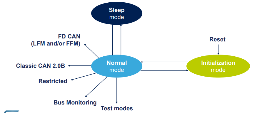
The following operation modes can be configured directly with the Mode option in the Cube:
- Normal mode
- Test mode, which is only used for production testing, self-test and calibration units
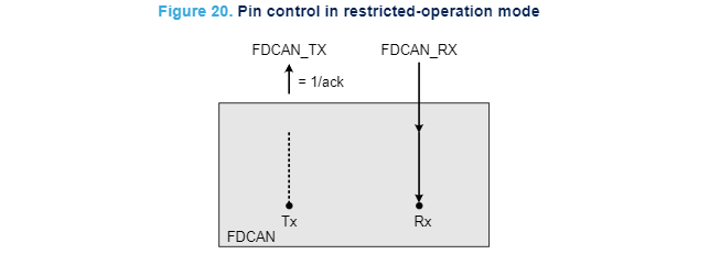
- Restricted operation mode, which can receive data frames / remote frames, confirm valid frames, and do not support sending (data / remote frames, active error frames, overload frames)
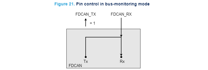
- Bus monitoring mode, which does not affect bus transmission, traffic analysis, can receive valid data frames / remote frames, and does not support transmission start / valid frame confirmation
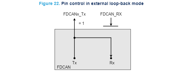
- External loop back mode, which is used for hardware self-test. FDCAN regards the messages sent by itself as received messages. If they are stored in Rx FIFO through reception filtering, FDCAN will ignore the confirmation error (implicit bit sampling in the confirmation slot) in order to be independent of external stimulation. The FDCAN performs internal feedback from its "send" output to its "receive" input.
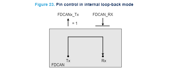
- Internal loop back mode, which is used for hardware self-test. Fdcan CAN be connected to fdcan without affecting_ TX and FDCAN_RXpins are tested with the CAN system running. FDCAN_RX pin is disconnected from fdcan and FDCAN_TX pin is in recessive state
Transceiver delay compensation TDC
There is such a code before CAN sends data:
     /* Configure and enable Tx Delay Compensation, required for BRS mode.
        TdcOffset default recommended value: DataTimeSeg1 * DataPrescaler
        TdcFilter default recommended value: 0 */
    HAL_FDCAN_ConfigTxDelayCompensation(&hfdcan1, 80, 0);
    HAL_FDCAN_EnableTxDelayCompensation(&hfdcan1);
12345
TDC, Transceiver delay compensation
At the sampling point, all transmitters check whether the previously transmitted bits are correctly sampled. This mechanism is needed to check for problems and detect other node error frames. Since the transmitter sees that its transmission bit is delayed due to the transceiver loop delay, the delay sets a lower limit for TSEG1, as shown in the figure below (the time period before the sampling point), which is also the upper limit of the data bit rate. This is why the transceiver delay compensation mechanism (TDC) is introduced
In order to compensate for this loop delay when checking bit errors, an auxiliary sampling point (SSP) is defined instead of operating at the sampling point, but checking the transmitted bits at the SSP. The results of this check are stored until the next sampling point is reached.
In the data phase, an SSP is generated for each transmitted bit. For the SSP position, the asymmetry and ringing of the transceiver should be considered, but since the transceiver monitors its own bit stream, there is no clock tolerance.
By writing 1 to FDCAN_ The TDC bit in dbtp enables transceiver delay compensation. Before the start of the data phase (at the falling edge of FDF bit to res), the measurement is started within each transmitted FDCAN frame. When in the "receive" input pin of the transmitter, FDCAN_ When this edge is seen on Rx, the measurement will stop. The resolution of the measurement is 1 mtq (minimum time quantum)
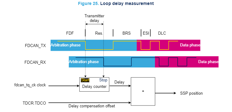
Delay compensation is always disabled during the arbitration phase. SSP location is defined as slave FDCAN_TX pin to fdcan_ The sum of the measured delay of Rx pin plus the transmitter delay compensation offset configured through TDCO [6:0] field
The transmitter delay compensation offset is used to adjust the position of the SSP inside the receive bit. Store the value of the transmitted bit until its SSP is reached, and then compare it with the actually received bit value
Clock calibration
FDCAN supports the function of clock calibration unit (CCU). This function allows the user to calibrate the FDCAN receiver (equipment) through the FDCAN transmitter (host). For example, when the FDCAN device communicates with the latest bit rate of the host, this function allows the user to add a new instance in the bus, and the existence of the bit rate is unknown. This is also useful when the FDCAN receiver does not have an accurate quartz (which may lead to a timing error).
CCU only operates when FDCAN bit rate is between 125 Kbit/s and 1 Mbit/s
Low power mode
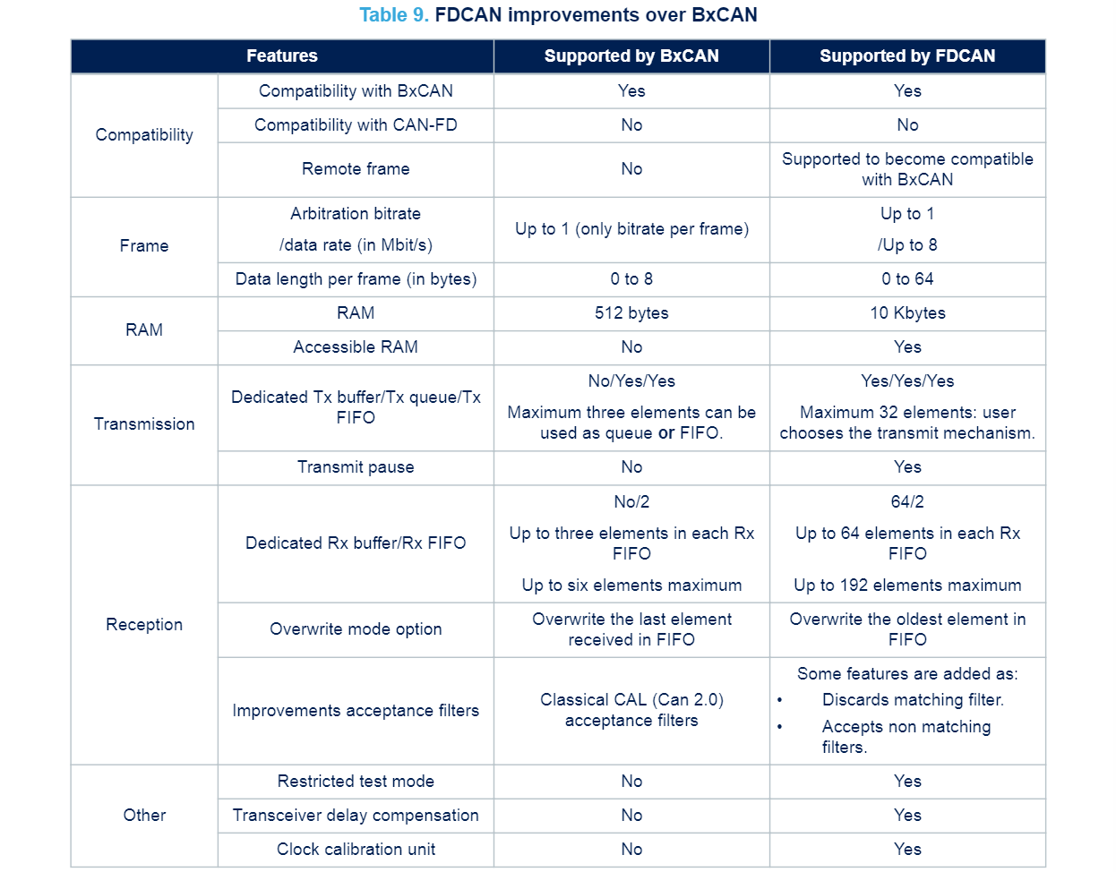
Upgrade existing BxCAN to CANFD
The following table helps users simplify the process of upgrading CAN 2.0 protocol in STM32 equipment to CAN-FD protocol: