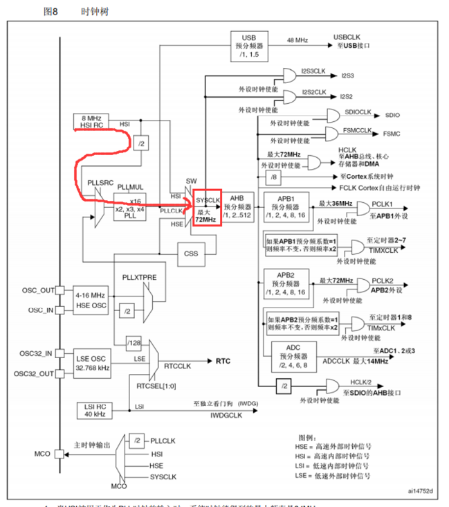
Overall design of STM32 clock
- Clock source: pure internal (inaccurate), internal and external (the oscillation circuit generated by the clock is internal, but the crystal oscillator is external), pure external (a clock is directly connected from the outside).
- There are several independent clocks inside the single chip microcomputer.
- PLL clock: phase locked loop circuit. The function is frequency doubling.
- There are two sets of independent clocks inside: HSx (high-speed clock source) and LSx (low-speed clock source).
- Pure internal: HSI, LSI.
- Internal and external; HSE,LSE.
- Pure external: OSC_IN,OSC32_IN (less used)
- SYSCLK in the red box is the system clock, which is the clock shared with the CPU (the CPU dominant frequency is the number of SYSCLK); The following part is to configure the clock of each module.
- After power on reset, the internal clock (red line path) is used by default (the internal clock is inaccurate)
STM32 clock register
- All clocks of STM32 are off by default when powered on (i.e. registers are 0 by default).
- In the following register diagram, the following r and w mean readable and writable (r: readable, set by hardware. w: writable) (rw: both readable and writable)
Clock control register (RCC_CR)
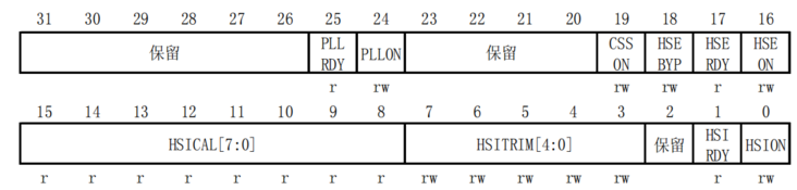
- PLLRDY: PLL clock ready flag. After PLL is locked, it is set to one by hardware. (PLL frequency doubling is not completed in an instant and takes a certain time) (0: PLL is not locked. 1: PLL is locked)
- PLLON: PLL is enabled, which is set to one and cleared by the software. When the PLL clock is used or selected to be used as the system clock, this bit cannot be cleared. (0: PLL off. 1: PLL enabled)
- HSERDY: external high speed clock ready flag. The hardware setting indicates that the external 4-16MHz oscillator has been stabilized. After the HSEON bit is cleared, this bit requires six external 4-25MHz oscillator cycles to be cleared. (0: not ready. 1: ready)
- HSEON: external high-speed clock enable. Set one and reset by software. (0: HSE oscillator off. 1: HSE oscillator on)
- HSIRDY: internal high speed clock ready flag. The hardware setting indicates that the internal 8MHz oscillator has been stabilized. After the HSION bit is cleared, this bit needs 6 internal 8MHz oscillator cycles to be cleared. (0: internal 8MHz oscillator is not ready, 1: internal 8MHz oscillator is ready)
- HSION: internal high speed clock enable. Set one and reset by software. (0: internal 8MHz oscillator off. 1: internal 8MHz oscillator on)
Clock configuration register (RCC_CFGR)
Note that it corresponds to the clock tree in the figure above.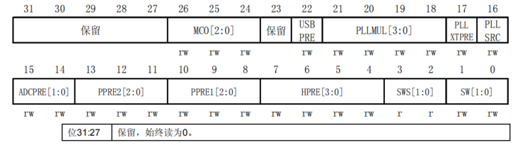
- USBPRE: USB prescaler. A 48MHz USB clock is generated by setting one or clearing zero by the software. In RCC_ Before enabling USB clock in apb1enr register, it must be ensured that this bit is valid. If the USB clock is enabled, this bit cannot be cleared. (0: PLL clock is divided by 1.5 times as USB clock. 1: PLL clock is directly used as USB clock)
- PLLMUL: PLL frequency doubling coefficient. The PLL frequency doubling coefficient is determined by software settings. It can only be written when PLL is off (Note: the output frequency of PLL cannot exceed 72MHz)
- PLLXTPRE: HSE frequency divider as PLL input. (set the software to one and clear to select whether to divide the frequency of HSE)
- PLLSRC: select PLL input clock source. (0: select HSI as PLL input clock after 2 frequency division. 1: select HSE clock as PLL input clock)
- ADCPRE: ADC prescaler. Set by software.
- PPRE2: high speed APB prescaler setting (APB2). The pre frequency division coefficient is set by the software.
- PPRE1: low speed APB prescaler setting (APB1). The pre frequency division coefficient is set by the software.
- HPRE: AHB prescaler. The pre frequency division coefficient is set by the software.
- Sw: system clock switching (SW position in the real-time clock tree). (00: HSI) (01: HSE) (10: PLL) (11: not available)
Clock interrupt register (RCC_CIR)
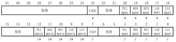
- PLLRDYC: clear PLL ready interrupt (1: clear PLL ready interrupt flag bit PLLRDYF)
- HSERDYC: clear HSE readiness interrupt (1: clear HSE readiness interrupt flag HSERDYF)
- HSIRDYC: clear HSI ready interrupt (1: clear HSI ready interrupt flag bit HSIRDYF)
- LSERDYC: clear LSE ready interrupt (1: clear LSE ready interrupt flag bit LSERDYF)
- LSIRDYC: clear LSI ready interrupt (1: clear LSI ready interrupt flag bit LSIRDYF)
- PLLRDYIE: PLL ready interrupt enable (1: HSE ready interrupt enable)
- HSIRDYIE: HSI ready interrupt enable (1: HSI ready interrupt enable)
- LSERDYIE: LSE ready interrupt enable (1: LSE ready interrupt enable)
- LSIRDYIE: LSI ready interrupt enable (1: LSI ready interrupt enable)
- PLLRDYF: PLL ready interrupt flag (when PLL is ready and PLLRDYIE bit is set to one, set to one by hardware)
- HSERDYF: HSE ready interrupt flag (when the external low-speed clock is ready and HSERDYIE bit is set to one, the hardware is set to one)
- HSIRDYF: HSI ready interrupt flag
- LSERDYF: LSE ready interrupt flag
- LSIRDYF: LSI ready interrupt flag
Code example
// Register macro definition
// The base address of RCC register is 0x40021000
#define RCC_ Base 0x40021000 / / base address of RCC partial register
#define RCC_ CR        (RCC_BASE + 0x00)    // RCC_ Address of Cr
#define RCC_CFGR    (RCC_BASE + 0x04)

#define FLASH_ACR    0x40022000

// Using C language to access the macro definition of register
#define rRCC_CR        (*((volatile unsigned int *)RCC_CR))
#define rRCC_CFGR    (*((volatile unsigned int *)RCC_CFGR))
#define rFLASH_ACR    (*((volatile unsigned int *)FLASH_ACR))

// Function function: switch the clock source to HSE and enable PLL, and set the main frequency to 72MHz
void Set_SysClockTo72M(void)
{
    unsigned int rccCrHserdy = 0;
    unsigned int rccCrPllrdy = 0;
    unsigned int rccCfrSwsPll = 0;
    unsigned int faultTime = 0;


    rRCC_CR = 0x00000083;        //Reset the clock to the initial power on state (HSI reset)

    //Turn on the external clock
    rRCC_CR &= ~(1<<16);      // Close HSEON
    rRCC_CR |= (1<<16);            // Open HSEON and let HSE work

    do
    {
        rccCrHserdy = rRCC_CR & (1<<17);    //Check whether the 17th bit is 1 (check whether the external high-speed clock is ready)
        faultTime++;//Timeout count
    }
    while ((faultTime<0x0FFFFFFF) && (rccCrHserdy==0));

    //The external clock is turned on successfully
    if ((rRCC_CR & (1<<17)) != 0)
    {
        rFLASH_ACR |= 0x10;
        rFLASH_ACR &= (~0x03);
        rFLASH_ACR |= (0x02);

        // Here, HSE is ready. Now go to match PLL and wait for him to be ready

        //Reset configuration register RCC_CFGR (APB and AHB do not divide frequency, and clock switching is not available)
        rRCC_CFGR &= (~((0x0f<<4) | (0x07<<8) | (0x07<<11)));
        // AHB and APB2 are not frequency divided, and APB1 is frequency divided by 2, so in the end: both AHB and APB2 are 72M, and APB1 is 36M
        rRCC_CFGR |= ((0x00<<4) | (0x04<<8) | (0x00<<11));


        rRCC_CFGR &= (~((1<<16) | (1<<17)));       // Clear bit17 and bit16
        rRCC_CFGR |= ((1<<16) | (0<<17));        // Select HSE as PLL input, and HSE does not divide frequency

        // Set the PLL frequency doubling coefficient to 9
        rRCC_CFGR &= (~(0x0f<<18));               // Reset bit18-21
        rRCC_CFGR |= (0x07<<18);                // 9 octave


        // Turn on the PLL switch
        rRCC_CR |= (1<<24);

        // The do while loop waits for the PLL clock to stabilize
        faultTime = 0;
        do
        {
            rccCrPllrdy = rRCC_CR & (1<<25);    //Check whether the 25th bit is 1
            faultTime++;//Detection time
        }
        while ((faultTime<0x0FFFFFFF) && (rccCrPllrdy==0));


        if ((rRCC_CR & (1<<25)) == (1<<25))
        {
          // This shows that the PLL clock has been stabilized and can be used. Now you can cut it

            // Switch PLL output to SYSCLK
            rRCC_CFGR &= (~(0x03<<0));
            rRCC_CFGR |= (0x02<<0);

            faultTime = 0;
            do
            {
                rccCfrSwsPll = rRCC_CFGR & (0x03<<2);    //Check whether the 25th bit is 1
                faultTime++;//Detection time
            }
            while ((faultTime<0x0FFFFFFF) && (rccCfrSwsPll!=(0x02<<2)));

               if ((rRCC_CFGR & (0x03<<2))== (0x02<<2))
            {
                // At this point, our clock has been set and can be over

            }
            else
            {
                // This shows that PLL output as SYSCLK is not successful
                while (1);
            }

        }
        else
        {
            // This means that there is an error in PLL startup, and PLL cannot work stably
            while (1);
        }

    }
    else
    {
        // HSE configuration timeout indicates that HSE is unavailable, and there is a problem with general hardware, which should be checked
        while (1);
    }
}