preface
This paper briefly introduces different ways to realize water lamp, and compares the similarities and differences under different ways.
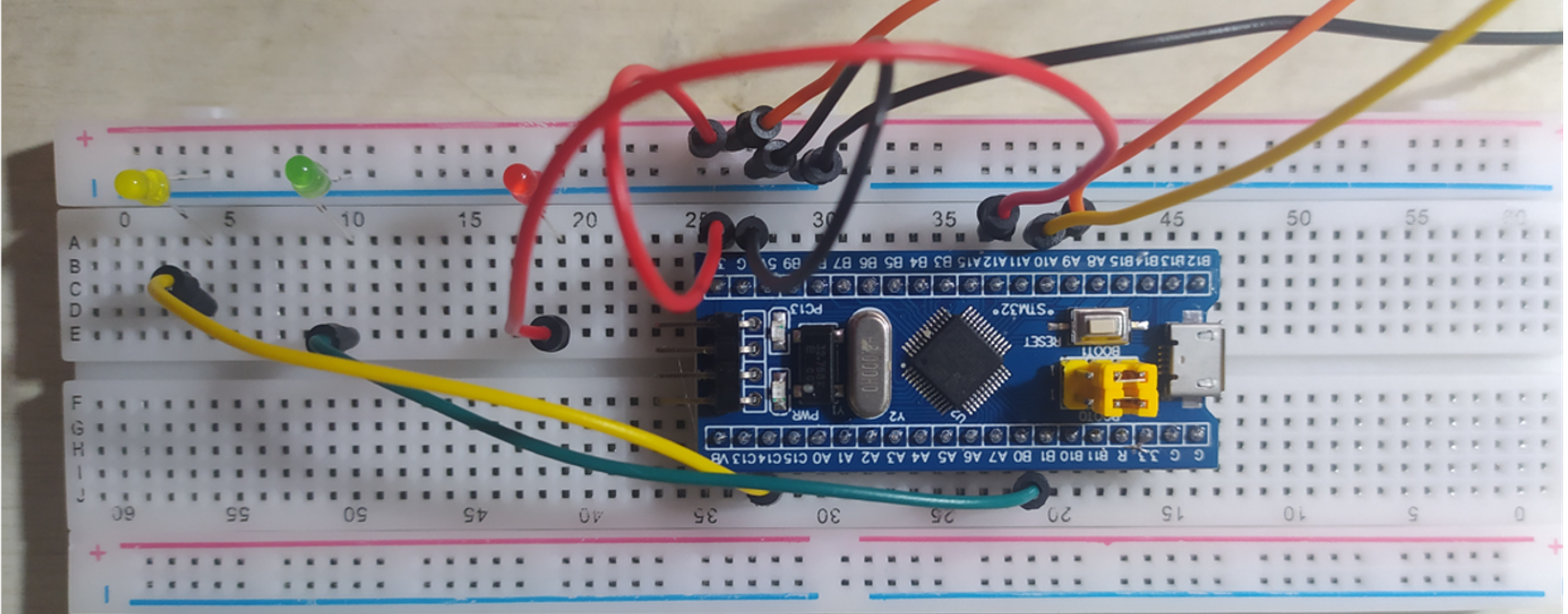
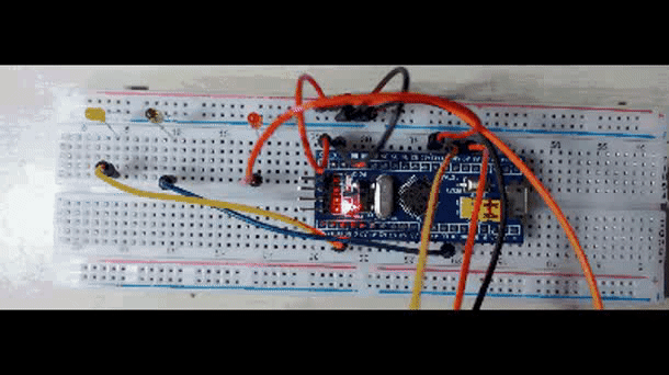
The circuit is built with STM32 minimum system core board (STM32F103C8T6) + panel board + 3 red, green and blue LEDs. The three ports of GPIOA, GPIOB and GPIOC are used to control the LED lights to flash in turn, with an interval of 1 second.
Here we use GPIOA_Pin_12,GPIOB_Pin_1,GPIOC_Pin_14 control red, green and blue LED lights respectively.
1, Firmware library water lamp
(1) New project
Because the ST firmware library is used, the configuration of this part is cumbersome. For details, please refer to some online configuration processes
Establishment of stm32f103c8t6 engineering template
The project document template and reference manual configured by me are also placed later for reference
(2) Configure GPIO ports
Three steps for initialization and setting of GPIO port
- Clock configuration
- Input / output mode setting
- Maximum rate setting
Let's follow this step to start configuring GPIOB_Pin_0 port
stm32 provides a firmware library encapsulated in c language. We can directly call the corresponding library functions for what functions we want to achieve.
- Configure clock
RCC_APB2PeriphClockCmd(RCC_APB2Periph_GPIOB, ENABLE); //Turn on the clock of the peripheral GPIOB
- GPIO initialization structure
The library function provides a structure to configure the input / output mode setting and maximum rate setting of GPIO port
as follows
typedef struct
{
  uint16_t GPIO_Pin;             /*!< Specifies the GPIO pins to be configured.
                                      This parameter can be any value of @ref GPIO_pins_define */

  GPIOSpeed_TypeDef GPIO_Speed;  /*!< Specifies the speed for the selected pins.
                                      This parameter can be a value of @ref GPIOSpeed_TypeDef */

  GPIOMode_TypeDef GPIO_Mode;    /*!< Specifies the operating mode for the selected pins.
                                      This parameter can be a value of @ref GPIOMode_TypeDef */
}GPIO_InitTypeDef;
- It is configured as universal push-pull output with an output speed of 2M
    GPIO_InitTypeDef   GPIO_InitStruct;

	GPIO_InitStruct.GPIO_Mode=GPIO_Mode_Out_PP;  			//The output mode is universal push-pull output
	GPIO_InitStruct.GPIO_Pin=GPIO_Pin_0 ;             //The selected port is GPIO_ Pin_ one
	GPIO_InitStruct.GPIO_Speed=GPIO_Speed_2MHz;				//The output speed is 2M

	GPIO_Init(GPIOB,&GPIO_InitStruct);
One GPIO_Pin_0 configuration completed.
Due to the high repeatability of this part of the code, you can write your own function to encapsulate the appeal process to achieve code simplicity.
Therefore, I put the relevant functions of water lamp in led.c and declare them in led.h.
(3) Improve the project and build the circuit
- Other functions
After the GPIO port is configured, we can control the led to turn on and off. However, if we need to achieve an accurate delay of 1s and the LED flashes, we need to add a delay function. There is no more introduction to this part of the system interrupt.
Software delay (no operation during cyclic operation) can also be used here. The disadvantage is that it can not achieve accurate delay and low operation efficiency.
- Build circuit
This time, we use c8t6 to control the red, green and yellow lights on the bread board to flash in turn. The circuit diagram is as follows.
2, Register flow lamp
(1) Register mapping
1. Learn to find register address
Take gpiob - > CRL register as an example, find the register address in stm32f103x Chinese reference manual
-
Find the starting address of the GPIOB port
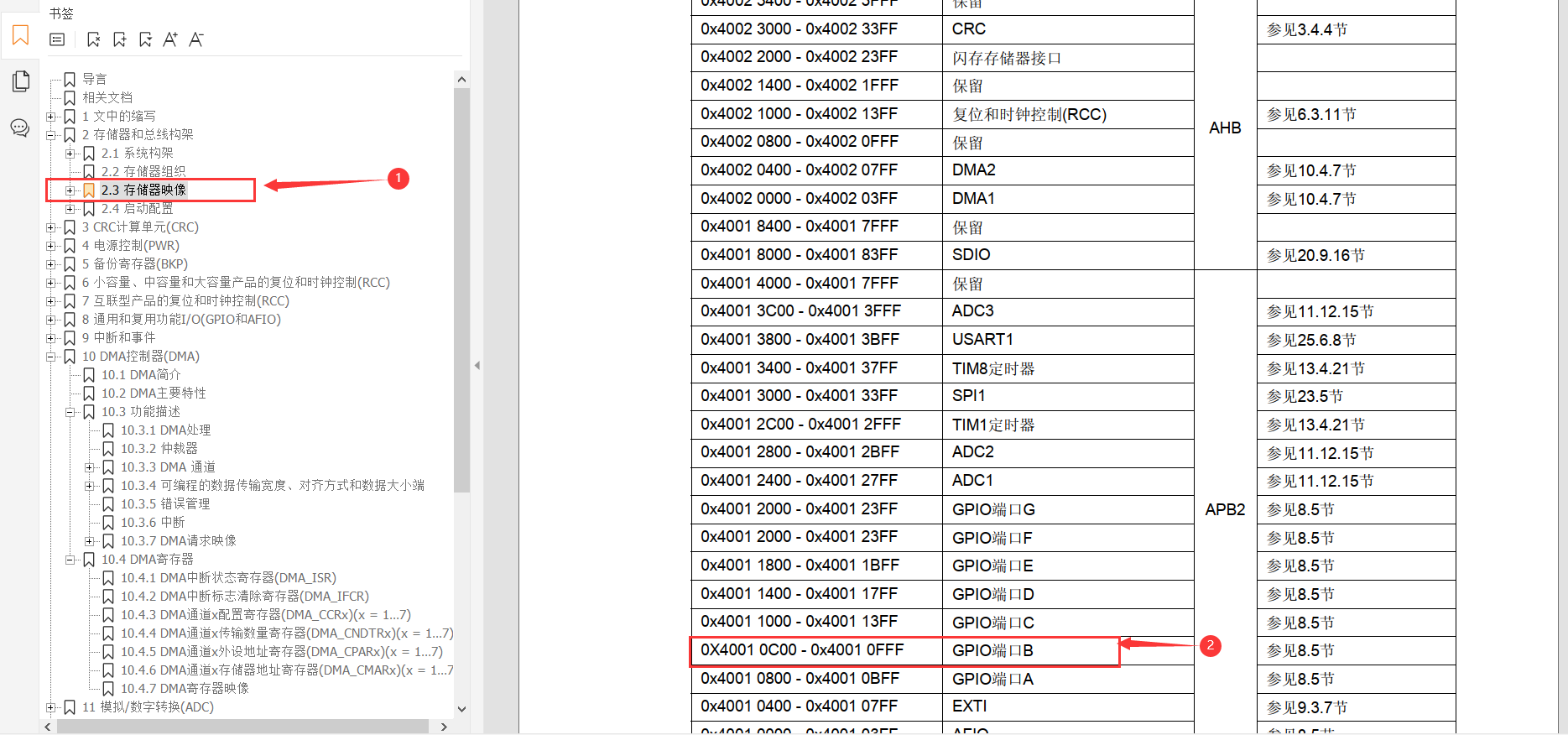
You can see that the starting address of GPIOB port is 0X4001 0C00 -
Locate the port configuration low register (GPIOx_CRL) in the GPIO register
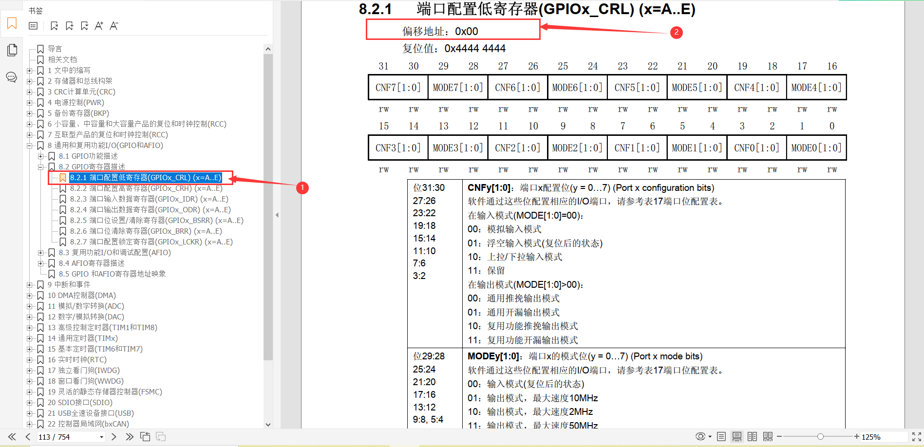
The offset address of the register is 0x00, so the address of GPIOB - > CRL is (starting address of GPIOB port + offset address) 0X4001 0C00+0x00=0X4001 0C00
2. Write other register addresses
Repeat the above steps to find the addresses of other required registers
/*RCC Peripheral base address*/
#define  RCC_BASE             (unsigned int)(0x40021000)
/*RCC The AHB1 clock enable register address is forcibly converted to a pointer*/
#define  RCC_APB2ENR		 *(unsigned int*)(RCC_BASE+0x18)

/*GPIOB Peripheral base address*/
#define  GPIOB_BASE           (unsigned int)(0X40010C00)

/* GPIOB Register address, cast to pointer */
#define GPIOB_CRL			*(unsigned int*)(GPIOB_BASE+0x00)
#define GPIOB_CRH			*(unsigned int*)(GPIOB_BASE+0x04)
#define GPIOB_IDR			*(unsigned int*)(GPIOB_BASE+0x08)
#define GPIOB_ODR			*(unsigned int*)(GPIOB_BASE+0x0C)
#define GPIOB_BSRR	        *(unsigned int*)(GPIOB_BASE+0x10)
#define GPIOB_BRR			*(unsigned int*)(GPIOB_BASE+0x14)
#define GPIOB_LCKR		    *(unsigned int*)(GPIOB_BASE+0x18)

/*GPIOC Peripheral base address*/
#define GPIOC_BASE           (unsigned int)(0x40011000)

/* GPIOC Register address, cast to pointer */
#define GPIOC_CRL			*(unsigned int*)(GPIOC_BASE+0x00)
#define GPIOC_CRH			*(unsigned int*)(GPIOC_BASE+0x04)
#define GPIOC_IDR			*(unsigned int*)(GPIOC_BASE+0x08)
#define GPIOC_ODR			*(unsigned int*)(GPIOC_BASE+0x0C)
#define GPIOC_BSRR	        *(unsigned int*)(GPIOC_BASE+0x10)
#define GPIOC_BRR			*(unsigned int*)(GPIOC_BASE+0x14)
#define GPIOC_LCKR		    *(unsigned int*)(GPIOC_BASE+0x18)


/*GPIOC Peripheral base address*/
#define GPIOD_BASE            (unsigned int)(0x40011400)

/* GPIOC Register address, cast to pointer */
#define GPIOD_CRL			*(unsigned int*)(GPIOD_BASE+0x00)
#define GPIOD_CRH			*(unsigned int*)(GPIOD_BASE+0x04)
#define GPIOD_IDR			*(unsigned int*)(GPIOD_BASE+0x08)
#define GPIOD_ODR			*(unsigned int*)(GPIOD_BASE+0x0C)
#define GPIOD_BSRR	        *(unsigned int*)(GPIOD_BASE+0x10)
#define GPIOD_BRR			*(unsigned int*)(GPIOD_BASE+0x14)
#define GPIOD_LCKR		    *(unsigned int*)(GPIOD_BASE+0x18)
The above includes all the registers involved in this experiment. The macro definition is used here to make the code more readable. The macro of the register name is defined as the address corresponding to the register, otherwise it has been operating against the address. Later, I don't know which register to operate.
(2) Function of register
Since register programming is involved, it is important for us to understand the role of relevant registers to be used.
To configure GPIOB_Pin_1 is the general push-pull output mode as an example
- APB2 peripheral clock enable register (RCC_APB2ENR)
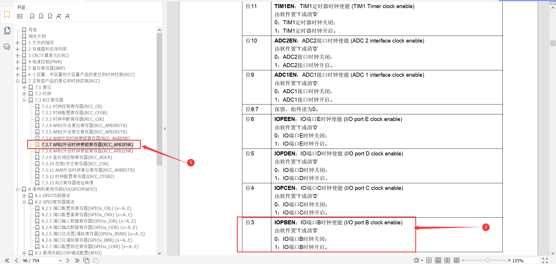
There are many peripherals in STM32. In order to reduce power consumption, each peripheral corresponds to a clock. These clocks are turned off when the chip is just powered on. If you want the peripherals to work, you must turn on the corresponding clock.
The function of this register is to control the switches of all peripheral clocks attached to APB2 bus. For each peripheral, we must turn on the corresponding clock. Here we can see RCC_ Bit 3 of the apb2enr register controls the clock on and off of the GPIOB.
-Turn on the clock of GPIOB peripheral
RCC_APB2ENR |= (1<<3); //Shift 1 left 3 bits to 0x10, and RCC_APB2ENR performs or operation
- Port configuration low register (GPIOx_CRL)
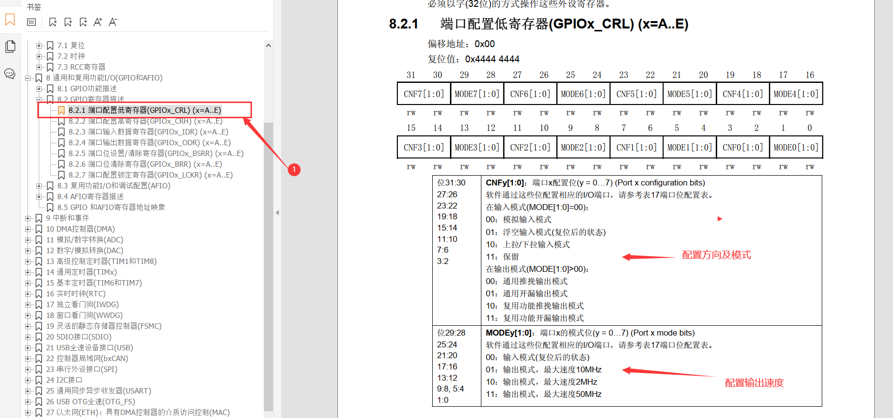
GPIOx_CRL contains pins 0-7 (control GPIO low 8 bits), and each pin occupies 4 register bits. The MODE bit is used to configure the output speed, and the CNF bit is used to configure various input and output modes.
We configure GPIOB_Pin_1 is universal push-pull output, and the output speed is 2M
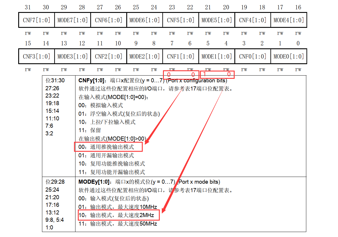
    GPIOB_CRL &= ~( 0x0F<< (4*1));// 0x0F shifts left by 4 bits, reverses, and then connects with GPIOB_CRL performs and operation to change the data of 4-7 bits to 0
	GPIOB_CRL |= (2<<4*0);   //2 shift 0 bit to the left and 0x02, set the second position to 1, configure PB1 as general push-pull output, and the speed is 2M
- Port output data register (GPIOx_ODR)
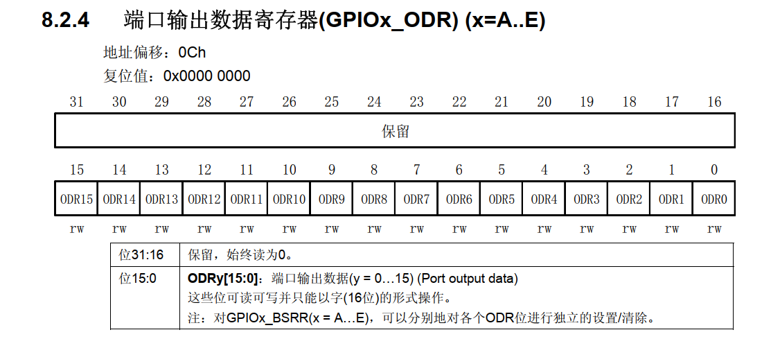
The function of this register is very simple. It controls the output data to 0 or 1.
Therefore, it is also very simple for us to control the LED delay flashing, that is, to control the ODR register to output 1 first, the LED light is on, delay for a period of time, control the ODR register to output 0 first, the LED light is off, and keep cycling, so as to realize the effect of running water lamp.
Control GPIOB_Pin_1 output is 1
GPIOB_ODR |= (1<<1); //1 shifts left by 1 bit and becomes 0x10, which is consistent with gpiob_ The ODR performs an or operation to change its second bit to 1
Control GPIOB_Pin_1 output is 0
GPIOB_ODR &= ~(1<<1); 1 Shift left by 1 bit and reverse,And GPIOB_ODR Performs an and operation to change its second bit to 0
(3) Register programming
- The total code is as follows
void delay(unsigned int i);

int main(void)
{
	// Turn on the clock of GPIOA, GPIOB and GPIOC ports
	RCC_APB2ENR |= (7<<2);

	//Clear the port bit of control PA12
	GPIOA_CRH &= ~( 0x0F<< (4*4));
	// PA12 is configured as universal push-pull output with a speed of 2M
	GPIOA_CRH |= (2<<4*4);


	//Clear the port bit of control PB1
	GPIOB_CRL &= ~( 0x0F<< (4*1));
	// PB1 is configured as universal push-pull output with a speed of 2M
	GPIOB_CRL |= (2<<4*1);


	//Clear the port bit of control PC14
	GPIOC_CRH &= ~( 0x0F<< (4*6));
	// PC14 is configured as universal push-pull output with a speed of 2M
	GPIOC_CRH |= (2<<4*6);

	while(1)
	{
		GPIOB_ODR |= (1<<1);
		delay(100);                 //Red flashing
	  GPIOB_ODR &= ~(1<<1);
	  delay(100);

		GPIOA_ODR |= (1<<12);
		delay(100);					//The yellow light flashes
	  GPIOA_ODR &= ~(1<<12);
	  delay(100);

		GPIOC_ODR |= (1<<14);
		delay(100);					//The green light flashes
	  GPIOC_ODR &= ~(1<<14);
	   delay(100);
	}

}


void delay(unsigned int i)
{
	unsigned char j;               //Simple delay function
	unsigned char k;
	for(;i>0;i--)
		for(j =500; j>0; j--)
	       for(k =200; k>0; k--);
}
Note: 4 * 0 is used in this code because it is used for GPIO_CRL(GPIO_CRL controls one pin every four bits). After changing 0 in 4 * 0 to 1, it is convenient to operate the subsequent pins. This writing method is for the convenience of subsequent operations.
When writing your own code, don't ignore the register address defined above.
3, Assembly language water lamp
-
When building a pure assembly project file and configuring the project file environment, do not select 'startup' and 'core' (because the reference program has its own functions such as startup file, which will lead to conflict after selection)
-
The code is as follows
RCC_APB2ENR EQU 0x40021018

GPIOA_CRH EQU   0x40010804
GPIOA_ODR EQU   0x4001080C

GPIOB_CRL EQU   0x40010C00    ;Register mapping
GPIOB_ODR EQU   0x40010C0C

GPIOC_CRH EQU   0x40011004
GPIOC_ODR EQU   0x4001100C


Stack_Size      EQU     0x00000400

                AREA    STACK, NOINIT, READWRITE, ALIGN=3
Stack_Mem       SPACE   Stack_Size
__initial_sp

                AREA    RESET, DATA, READONLY

__Vectors       DCD     __initial_sp
                DCD     Reset_Handler


                AREA    |.text|, CODE, READONLY

                THUMB
                REQUIRE8
                PRESERVE8

                ENTRY
Reset_Handler


MainLoop		BL LED2_Init
                BL LED2_ON
                BL Delay             ;LED2 The lamp flashes
                BL LED2_OFF
                BL Delay

				BL LED1_Init
				BL LED1_ON
                BL Delay             ;LED1 The lamp flashes
                BL LED1_OFF
                BL Delay

                BL LED3_Init
				BL LED3_ON
                BL Delay            ;LED3 The lamp flashes
                BL LED3_OFF
                BL Delay

                B MainLoop


LED1_Init
                PUSH {R0,R1, LR}

                LDR R0,=RCC_APB2ENR
                ORR R0,R0,#0x08         ; Turn on the clock of port GPIOB
                LDR R1,=RCC_APB2ENR
                STR R0,[R1]


                LDR R0,=GPIOB_CRL
                ORR R0,R0,#0X00000020   ;GPIOB_Pin_1 is configured as a universal push-pull output
                LDR R1,=GPIOB_CRL
                STR R0,[R1]

                LDR R0,=GPIOB_ODR
                BIC R0,R0,#0X00000002
                LDR R1,=GPIOB_ODR          ;GPIO_Pin_1 The output is 0
                STR R0,[R1]

                POP {R0,R1,PC}


LED1_OFF
                PUSH {R0,R1, LR}

                LDR R0,=GPIOB_ODR
                BIC R0,R0,#0X00000002    ;GPIO_Pin_1 output is 0, LED1 is off
			    LDR R1,=GPIOB_ODR
                STR R0,[R1]

                POP {R0,R1,PC}

LED1_ON
                PUSH {R0,R1, LR}

                 LDR R0,=GPIOB_ODR
                ORR R0,R0,#0X00000002    ;GPIO_Pin_1 output is 1, LED1 is on
                 LDR R1,=GPIOB_ODR
                STR R0,[R1]
                POP {R0,R1,PC}


LED2_Init
                PUSH {R0,R1, LR}

                LDR R0,=RCC_APB2ENR
                ORR R0,R0,#0x04 		   ; Turn on the clock of GPIOA
                LDR R1,=RCC_APB2ENR
                STR R0,[R1]

                LDR R0,=GPIOA_CRH
                ORR R0,R0,#0X00020000   ;GPIOA_Pin_12 is configured as a universal push-pull output
                LDR R1,=GPIOA_CRH
                STR R0,[R1]

                LDR R0,=GPIOA_ODR
                BIC R0,R0,#0X00001000
                LDR R1,=GPIOA_ODR            ;GPIOA_Pin_12 The output is 0
                STR R0,[R1]

                POP {R0,R1,PC}

LED2_OFF
                PUSH {R0,R1, LR}

               LDR R0,=GPIOA_ODR
               BIC R0,R0,#0X00001000        ;GPIOA_Pin_12 output is 0, LED2 is off
			    LDR R1,=GPIOA_ODR
                STR R0,[R1]

                POP {R0,R1,PC}

LED2_ON
                PUSH {R0,R1, LR}

                LDR R0,=GPIOA_ODR
                ORR R0,R0,#0X00001000     ;GPIOA_Pin_12 output is 1, LED2 is on
				 LDR R1,=GPIOA_ODR
                STR R0,[R1]

				 POP {R0,R1,PC}


LED3_Init
                PUSH {R0,R1, LR}

                LDR R0,=RCC_APB2ENR
                ORR R0,R0,#0x10 		    ; Turn on the clock of GPIOC
                LDR R1,=RCC_APB2ENR
                STR R0,[R1]

                LDR R0,=GPIOC_CRH
                ORR R0,R0,#0X02000000   ;GPIOC_Pin_14 is configured as a universal push-pull output
                LDR R1,=GPIOC_CRH
                STR R0,[R1]

                LDR R0,=GPIOC_ODR
                BIC R0,R0,#0X00004000   ;GPIOC_Pin_14 output is 0
                LDR R1,=GPIOC_ODR
                STR R0,[R1]

                POP {R0,R1,PC}

LED3_OFF
                PUSH {R0,R1, LR}

                LDR R0,=GPIOC_ODR
                BIC R0,R0,#0X00004000  ;GPIOC_Pin_14 output is 0, LED3 goes out
			    LDR R1,=GPIOC_ODR
                STR R0,[R1]

                POP {R0,R1,PC}

LED3_ON
                PUSH {R0,R1, LR}

                 LDR R0,=GPIOC_ODR
                ORR R0,R0,#0X00004000   ;GPIOC_Pin_14 output is 1, LED3 is on
                 LDR R1,=GPIOC_ODR
                STR R0,[R1]

                POP {R0,R1,PC}

Delay
                PUSH {R0,R1, LR}

                MOVS R0,#0
                MOVS R1,#0
                MOVS R2,#0

DelayLoop0
                ADDS R0,R0,#1

                CMP R0,#300
                BCC DelayLoop0

                MOVS R0,#0
                ADDS R1,R1,#1
                CMP R1,#300
                BCC DelayLoop0

                MOVS R0,#0
                MOVS R1,#0
                ADDS R2,R2,#1
                CMP R2,#15
                BCC DelayLoop0

                POP {R0,R1,PC}

                END
- About stm32 startup file
Stack_Size      EQU     0x00000400

                AREA    STACK, NOINIT, READWRITE, ALIGN=3
Stack_Mem       SPACE   Stack_Size
__initial_sp

                AREA    RESET, DATA, READONLY

__Vectors       DCD     __initial_sp
                DCD     Reset_Handler


                AREA    |.text|, CODE, READONLY

                THUMB
                REQUIRE8
                PRESERVE8

                ENTRY
Reset_Handler
We just said that we should not select the 'startup' startup file when creating a new project, because we have defined some functions about the startup ` 'startup file here. If the startup startup file is included, it will cause conflicts.
Brief introduction to 'startup' startup file
The startup file is written by assembly and is the first program to be executed after the system is powered on and reset. The main work is as follows:
- Initialize stack pointer SP=_initial_sp
- Initialize PC pointer = Reset_Handler
- Initialize interrupt vector table
- Configure system clock
- Call C library function_ Main initializes the user stack, and finally calls the main function to the world of C
- LED port initialization
LED1_Init
                PUSH {R0,R1, LR}

                LDR R0,=RCC_APB2ENR
                ORR R0,R0,#0x08       ; Turn on the clock of port GPIOB
                LDR R1,=RCC_APB2ENR
                STR R0,[R1]


                LDR R0,=GPIOB_CRL
                ORR R0,R0,#0X00000020   ;GPIOB_Pin_1 is configured as universal push-pull output, and the output speed is 2M
                LDR R1,=GPIOB_CRL
                STR R0,[R1]

                LDR R0,=GPIOB_ODR
                BIC R0,R0,#0X00000002   ; Configure GPIOB_Pin_1. The output is low level and the LED is off
                LDR R1,=GPIOB_ODR
                STR R0,[R1]

                POP {R0,R1,PC}
- Software delay
Delay
                PUSH {R0,R1, LR}

                MOVS R0,#0
                MOVS R1,#0
                MOVS R2,#0

DelayLoop0
                ADDS R0,R0,#1

                CMP R0,#300
                BCC DelayLoop0

                MOVS R0,#0
                ADDS R1,R1,#1
                CMP R1,#300
                BCC DelayLoop0

                MOVS R0,#0
                MOVS R1,#0
                ADDS R2,R2,#1
                CMP R2,#15
                BCC DelayLoop0

                POP {R0,R1,PC}
This part adopts software delay. The specific principle is that R0, R1 and R2 are initialized to 0, R0 plus 1. When R0 is greater than 300, R1 plus 1, then R0 becomes 0, R0 continues to add 1, and cycle. When R1 is greater than 300, R2 plus 1, R0 and R1 become 0. Continue this operation.
This delay function lasts about 300 * 300 * 15 = 1350000 instruction cycles.
- Summary
Some parts of the assembly code of this instance are repeated, resulting in some redundancy of the code. In addition, in fact, the lighting method I use is essentially operating registers, but I use assembly language. You can refer to the above register lighting program to compare the difference between the two.
For the convenience of comparison, I try to keep the naming of variables in the assembler the same as that in the register.
4, Actual effect
The above three methods are to control GPIOA_Pin_12 ,GPIOB_Pin_1,GPIOC_ Pin_ The final implementation results of port 14 are as follows.
summary
From c language firmware library to register to assembly language, this experiment involves more and more low-level, and has a deeper understanding of some functions of stm32 register.
In register operation, pointer and macro definitions are used for shift left, shift right, XOR, bitwise and, bitwise OR, as well as the structure of c language. It can be regarded as learning for practical use.
The deficiency of the experiment is that the precise delay is not used when using assembly language, but the second is to use the software delay with low accuracy. The reason is still unfamiliar.
I hope you will not hesitate to point out the inadequacies mentioned above.
reference resources
STM32 from address to register
STM32 register introduction, address search, and direct operation register
Reference books
STM32 Library Development Guide - wildfire based developer development board
STM32F10X reference manual
Data link
Link: https://pan.baidu.com/s/1w5iVrx-Ob_C5z5MljxZkww
Extraction code: i4wl