preface
Clock system is an essential part of MCU. This paper will discuss the following problems:
- What is a clock?
- How to understand the STM32 clock structure?
- Why does MCU have multiple clock sources?
- How does STM32 configure the clock?
catalogue
4, Clock configuration analysis
3.1. 1. Analysis of HSE status and normal conditions
3.1. 2 set the prescaler factor of AHB, APB1 and APB2
3.1. 3. Select the clock source of PLL
3.1. 4 turn on the PLL clock and wait for it to be ready (wait when it is turned on)
3.1. 5. Select PLL as the system clock source (the same is true by default)
5.1 clock configuration process
5.2 learn the clock flow of an MCU
1, Clock introduction
First of all, we have to clarify several concepts:
- Clock: the heart of single chip microcomputer. The operation of all peripherals requires clock energy.
- Clock cycle: also known as oscillation cycle, it can be simply understood as the time required to transmit a 0 or 1
- Instruction cycle: the time required to execute an instruction (such as MOV A, #34H). The instruction cycle length may be different for different types of instructions.
- Machine cycle: the time period during which an action is performed. For example, to execute an instruction, two actions are required: "fetch instruction and decode" and "execute operand".
The relationship diagram of the above three cycles is as follows: (the figure is reproduced)
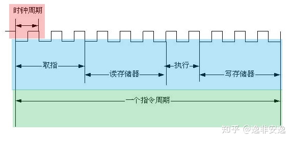
(the blue part includes four machine cycles)
Because the clock signal is also a kind of electrical signal, it also plays the role of energy supply, and the time interval due to level change is certain, We can even use the clock to count time (PS: the statement of "clock energy supply" here is wrong, and the clock can not play the role of energy supply, but I think it is not a big problem for beginners to understand this sensibility. Only remember that the clock does not provide energy)
2, STM32 clock tree
With the above perceptual understanding, let's take a look at the clock tree of STM32F10X:
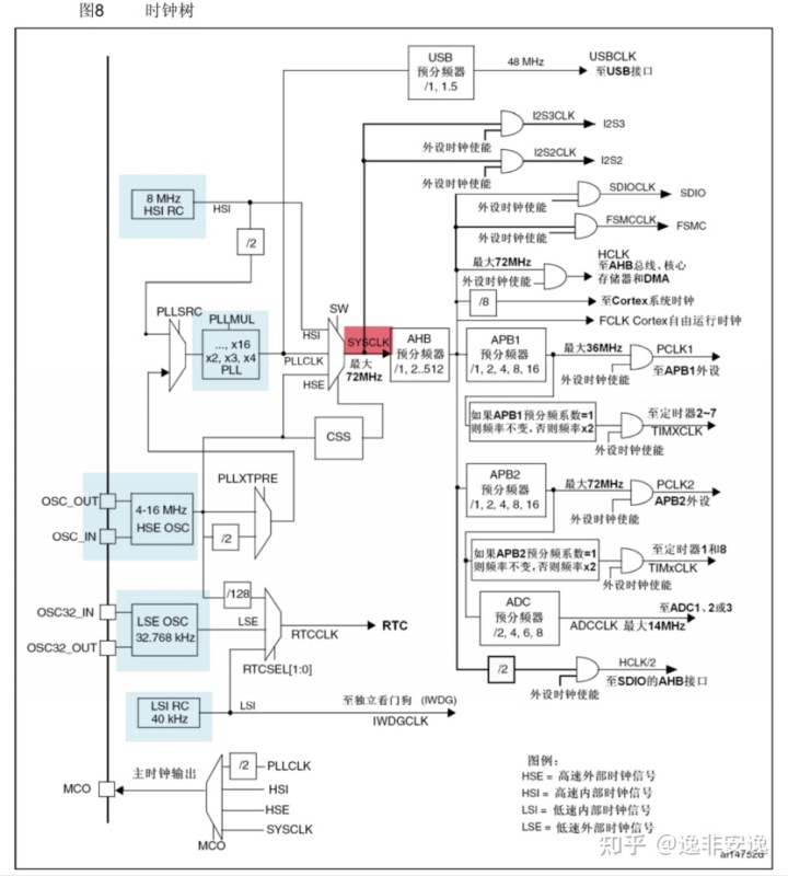
2.1 STM32F10X clock source
The blue part of the figure above shows the five clock sources of STM32, which are:
- HSI: High Speed Internal clock, generated by the internal RC oscillator of the chip, with a frequency of 8MHZ
- HSE: High Speed External clock, which can be connected with 4-16MHZ crystal oscillator as clock source
- LSE: low speed external clock, external 32.768KHZ clock source
- LSI: low speed internal clock, generated by the RC oscillator inside the chip, with a frequency of 40KHZ
- PLL: PLL frequency doubling output. It can achieve frequency doubling output 2-16 times of the input clock
PS: PLL is also listed as the clock source here by referring to the statements such as punctual atoms and wildfire data. Personally, I think the actual clock source can only be counted as four strictly, because PLL itself only plays the role of frequency doubling and cannot generate clock frequency itself. Of course, these are artificially defined, which will not affect the use and understanding of the knowledge point, and help to understand the knowledge.
2.2 system clock
After knowing the clock sources, we can find that the clock tree is actually the well-known AHB, APB1 and APB2 buses
The clock source and these peripherals are connected together through the system clock SYSCLK in the red part. Therefore, the system clock SYSCLK is very important!!!
It can be seen that the system clock has three input sources:
- HSI: 8MHZ
- PLLCLK: 8-128MHZ (external crystal oscillator is generally 8MHZ)
- HSE: 4-16MHZ
The maximum frequency that SYSCLK can accept is 72MHZ, which is also the frequency at which all peripherals can operate normally.
It can be seen that if you want to reach this number, you can only get it through PLL frequency doubling (you can also use it to overclock)
By the way, SYSCLK selects something that is also connected with CSS. You can know CSS (clock security system) by checking the data manual
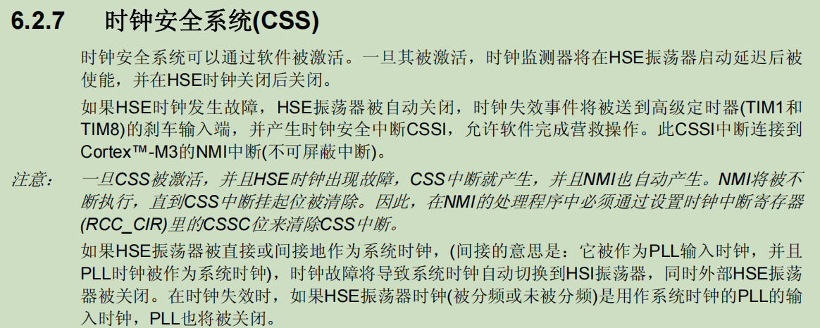
As you can see, this thing is simply an alarm. Help you check whether there is any problem with HSE. If so, first switch to the internal clock source HSI, and then prompt relevant information.
After analysis, we can have a relatively clear understanding of the STM32 clock tree: the clock source, then configure the bus clock (AHB, APB1, APB2), and finally mount the clock of the peripheral on the specific bus on the bus clock
The following points are added:
- Low speed internal and external clock applications (LSI and LSE)
The low-speed clock LSI and LSE can also be seen from the clock tree diagram. Both of them can be used as the clock source of RTC (real-time clock), and the frequency division of HSE can also be used. In addition, LSI can be used as an independent watchdog clock
- MCO clock output: it is used to observe the clock signal and adjust the oscilloscope. In short, it can measure the frequency of the clock source and directly watch the waveform
3, Some thoughts on clock
3.1 clock frequency
From the discussion of 2.1 and 2.2, we can find that the clock frequency of the system clock is 72MHZ. However, the actual input system clock frequency can reach 128MHZ at most and 8MHZ at least, which means that we can do some "illegal operations" without following the provisions of the data manual
The answers I found on the Internet are:
- When the frequency is high, the system stability will be affected. Specifically, during communication, the peripherals may not receive accurate signals and the power consumption will increase
- The frequency is too low to meet the frequency requirements of the equipment, and the equipment may not be started
3.2 multiple clock sources
You may have such a question when you first contact the clock. Why do you need so many clock sources, including internal clock sources and external clock sources? All peripherals are managed by the system clock. Isn't it enough to use only one clock?
Based on the above questions, through reading the materials and online answers, two obvious conclusions are obtained:
- Multiple clock sources can play an emergency role when a single clock source fails
- A peripheral has multiple clock sources, and the clock source of corresponding frequency can be selected as required
4, Clock configuration analysis
After understanding the STM32 clock tree, it is the problem of clock configuration.
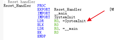
In fact, when we create the project import startup file, the startup file has called the SystemInit function to initialize the system clock before the main function is called. (here are the five functions of the startup file: setting the stack pointer, setting the PC pointer, initializing the interrupt vector table, configuring the system clock, calling the C library function _main, and finally going to the C world).
Then why do I need to do configuration analysis? Just use it directly?
Regardless of other chips, let's just look at the library functions provided by stm32's firmware library (the screenshot of system_stm32f10x.c below):
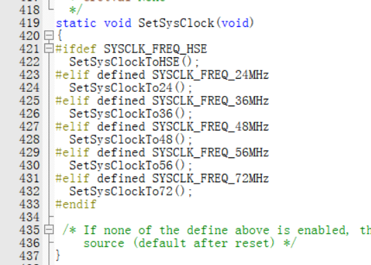
People's ST official only provides system clock settings of 24MHz, 36MHz, 48MHz, 56MHz and 72MHz.
If the project needs clocks beyond these five frequencies, you still have to do it yourself. For the above reasons, the analysis of clock configuration is just needed.
Then, let's look at the diagram of the clock tree and sort out the context of the system clock.
Input source:
- HSI is output directly, and the frequency is only 8MHz.
- HSE direct output, range 4-16MHz, generally 8MHz.
- PLL: PLL frequency doubling output, and the frequency doubling range is 2-16 times. And the PLL itself has two input sources:
- HSI dichotomy output to PLL. The system clock in this way can be up to 64MHz.
- HSE is output directly to PLL.
Output source:
- Direct output.
- It is output to AHB bus and can be divided by 1 ~ 512 through prescaler.
- After pre frequency division of AHB bus, it passes through low-speed peripheral bus APB1 and high-speed bus APB2.
Considering the problem of power consumption, the peripheral will turn on the clock only when it is used, so SYSCLK only needs to initialize the bus clock.
For this reason, the process of system clock configuration can be summarized as follows:
1. Select and turn on the clock source (if PLL is used as the system clock source, you also need to select the frequency doubling coefficient)
2. Select the prescaler coefficients of APB1, APB2 and AHB
I think there must be someone here like me. When I first learned, I had such doubts. Why did you jump from the left to the right of the clock tree all at once? It's almost illogical (cnm), but it's not
If AHB is turned on first and APB1 and APB2 are not set, disorder will occur
The following takes the library function {SetSysClockTo72() as an example to learn the configuration process with the data manual. First paste the source code:
* @brief Sets System clock frequency to 72MHz and configure HCLK, PCLK2
* and PCLK1 prescalers.
* @note This function should be used only after reset.
* @param None
* @retval None
*/
static void SetSysClockTo72(void)
{
__IO uint32_t StartUpCounter = 0, HSEStatus = 0;
/* SYSCLK, HCLK, PCLK2 and PCLK1 configuration ---------------------------*/
/* Enable HSE */
RCC->CR |= ((uint32_t)RCC_CR_HSEON);
/* Wait till HSE is ready and if Time out is reached exit */
do
{
HSEStatus = RCC->CR & RCC_CR_HSERDY;
StartUpCounter++;
} while((HSEStatus == 0) && (StartUpCounter != HSE_STARTUP_TIMEOUT));
if ((RCC->CR & RCC_CR_HSERDY) != RESET)
{
HSEStatus = (uint32_t)0x01;
}
else
{
HSEStatus = (uint32_t)0x00;
}
if (HSEStatus == (uint32_t)0x01)
{
/* Enable Prefetch Buffer */
FLASH->ACR |= FLASH_ACR_PRFTBE;
/* Flash 2 wait state */
FLASH->ACR &= (uint32_t)((uint32_t)~FLASH_ACR_LATENCY);
FLASH->ACR |= (uint32_t)FLASH_ACR_LATENCY_2;
/* HCLK = SYSCLK */
RCC->CFGR |= (uint32_t)RCC_CFGR_HPRE_DIV1;
/* PCLK2 = HCLK */
RCC->CFGR |= (uint32_t)RCC_CFGR_PPRE2_DIV1;
/* PCLK1 = HCLK */
RCC->CFGR |= (uint32_t)RCC_CFGR_PPRE1_DIV2;
#ifdef STM32F10X_CL
/* Configure PLLs ------------------------------------------------------*/
/* PLL2 configuration: PLL2CLK = (HSE / 5) * 8 = 40 MHz */
/* PREDIV1 configuration: PREDIV1CLK = PLL2 / 5 = 8 MHz */
RCC->CFGR2 &= (uint32_t)~(RCC_CFGR2_PREDIV2 | RCC_CFGR2_PLL2MUL |
RCC_CFGR2_PREDIV1 | RCC_CFGR2_PREDIV1SRC);
RCC->CFGR2 |= (uint32_t)(RCC_CFGR2_PREDIV2_DIV5 | RCC_CFGR2_PLL2MUL8 |
RCC_CFGR2_PREDIV1SRC_PLL2 | RCC_CFGR2_PREDIV1_DIV5);
/* Enable PLL2 */
RCC->CR |= RCC_CR_PLL2ON;
/* Wait till PLL2 is ready */
while((RCC->CR & RCC_CR_PLL2RDY) == 0)
{
}
/* PLL configuration: PLLCLK = PREDIV1 * 9 = 72 MHz */
RCC->CFGR &= (uint32_t)~(RCC_CFGR_PLLXTPRE | RCC_CFGR_PLLSRC | RCC_CFGR_PLLMULL);
RCC->CFGR |= (uint32_t)(RCC_CFGR_PLLXTPRE_PREDIV1 | RCC_CFGR_PLLSRC_PREDIV1 |
RCC_CFGR_PLLMULL9);
#else
/* PLL configuration: PLLCLK = HSE * 9 = 72 MHz */
RCC->CFGR &= (uint32_t)((uint32_t)~(RCC_CFGR_PLLSRC | RCC_CFGR_PLLXTPRE |
RCC_CFGR_PLLMULL));
RCC->CFGR |= (uint32_t)(RCC_CFGR_PLLSRC_HSE | RCC_CFGR_PLLMULL9);
#endif /* STM32F10X_CL */
/* Enable PLL */
RCC->CR |= RCC_CR_PLLON;
/* Wait till PLL is ready */
while((RCC->CR & RCC_CR_PLLRDY) == 0)
{
}
/* Select PLL as system clock source */
RCC->CFGR &= (uint32_t)((uint32_t)~(RCC_CFGR_SW));
RCC->CFGR |= (uint32_t)RCC_CFGR_SW_PLL;
/* Wait till PLL is used as system clock source */
while ((RCC->CFGR & (uint32_t)RCC_CFGR_SWS) != (uint32_t)0x08)
{
}
}
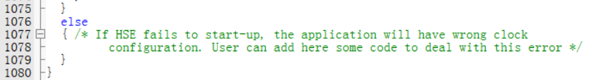
else
{ /* If HSE fails to start-up, the application will have wrong clock
configuration. User can add here some code to deal with this error */
}
}
#endif
At first glance, it looks very long and there are many registers, but it doesn't matter. First write down the registers that appear:
- RCC->CR
- RCC->CFGR
- RCC->CFGR2
- FLASH->ACR
Then what? Of course Search manual What are these registers for! Since it is still a new stage of Xiaomeng, you only need to understand the general function of each register above and study it in combination with the source code. There is no need to go into the manual for the time being.
Combined with the above understanding, let's analyze the source code paragraph by paragraph: (patiently look at the functions of each bit of the register in the reference manual)
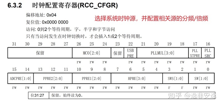
1. Start HSE clock
* SYSCLK, HCLK, PCLK2 and PCLK1 configuration ---------------------------*/
  /* Enable HSE */
  RCC->CR |= ((uint32_t)RCC_CR_HSEON);//HSEON -> HSE_ON
2. Wait until HSE is ready (there must be a part of time buffer stability due to clock oscillation and other reasons)
/* Wait till HSE is ready and if Time out is reached exit */
  do
  {
    HSEStatus = RCC->CR & RCC_CR_HSERDY;
    StartUpCounter++;
  } while((HSEStatus == 0) && (StartUpCounter != HSE_STARTUP_TIMEOUT));

  if ((RCC->CR & RCC_CR_HSERDY) != RESET)
  {
    HSEStatus = (uint32_t)0x01;
  }
  else
  {
    HSEStatus = (uint32_t)0x00;
  }
3. If the HSE status is normal, it will continue, and if it is abnormal, it will be handled immediately
If the status is abnormal, jump to the following through the conditional statement, and the user can define the exception handling by himself
3.1. 1. Analysis of HSE status and normal conditions
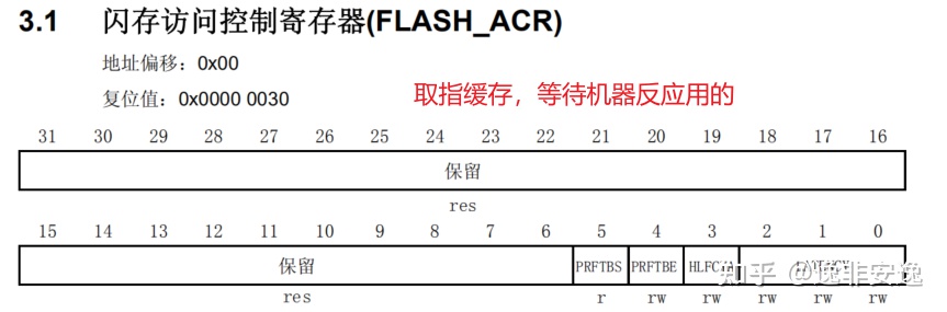
/* Enable Prefetch Buffer */
FLASH->ACR |= FLASH_ACR_PRFTBE;
/* Flash 2 wait state */
FLASH->ACR &= (uint32_t)((uint32_t)~FLASH_ACR_LATENCY);
FLASH->ACR |= (uint32_t)FLASH_ACR_LATENCY_2;
This involves the knowledge of FLASH programming. I think the explanation given by punctual atom is that the reaction speed of CPU is faster than that of FLASH, so you need to wait for two states. Wait for several States to see your clock configuration. You can see the FLASH programming manual, which explains (48-72MHZ is two state time)
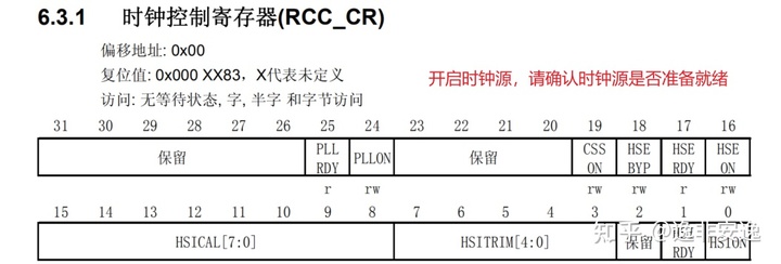
3.1. 2 set the prescaler factor of AHB, APB1 and APB2
/* HCLK = SYSCLK */
    RCC->CFGR |= (uint32_t)RCC_CFGR_HPRE_DIV1;

    /* PCLK2 = HCLK */
    RCC->CFGR |= (uint32_t)RCC_CFGR_PPRE2_DIV1;

    /* PCLK1 = HCLK */
    RCC->CFGR |= (uint32_t)RCC_CFGR_PPRE1_DIV2;
3.1. 3. Select the clock source of PLL
In fact, there are twenty or thirty lines of code in the source code, but that is the configuration code of interconnected chips. Here f103 is the basic type, so I'll skip it for the time being.
/* PLL configuration: PLLCLK = HSE * 9 = 72 MHz */
RCC->CFGR &= (uint32_t)((uint32_t)~(RCC_CFGR_PLLSRC | RCC_CFGR_PLLXTPRE |
RCC_CFGR_PLLMULL));
/* HSE 72MHz system clock output with PLLMULL9 */
RCC->CFGR |= (uint32_t)(RCC_CFGR_PLLSRC_HSE | RCC_CFGR_PLLMULL9);
3.1. 4 turn on the PLL clock and wait for it to be ready (wait when it is turned on)
/* Enable PLL */
RCC->CR |= RCC_CR_PLLON;
/* Wait till PLL is ready */
while((RCC->CR & RCC_CR_PLLRDY) == 0)
{
}
3.1. 5. Select PLL as the system clock source (the same is true by default)
/* Select PLL as system clock source */
RCC->CFGR &= (uint32_t)((uint32_t)~(RCC_CFGR_SW));
RCC->CFGR |= (uint32_t)RCC_CFGR_SW_PLL;
/* Wait till PLL is used as system clock source */
while ((RCC->CFGR & (uint32_t)RCC_CFGR_SWS) != (uint32_t)0x08)
{
}
5, Summary
5.1 clock configuration process
- Turn on the clock and wait for ready
- Exit if the clock is abnormal (the user can handle relevant exceptions by himself)
- If it turns on normally, configure the pre frequency division coefficient of the relevant bus first
- Finally, select whether the system clock is PLL or HSI or HSE to let the peripherals get the clock
5.2 learn the clock flow of an MCU
- Looking at the clock tree -- analyzing the context of the clock
- Check the data manual and find the answers to the following questions:
- How to turn on the clock source?
- How to control the clock of related peripherals
- How to select the system clock source
Finally, the theory gives practice. Configure another clock by yourself or write a clock configuration function by yourself. Please refer to my writing method of clock configuration function based on firmware library function (the official configuration of ST is based on register programming)