1, Design ideas
This experiment uses GPIOB, GPIOC and GPIOD to control LED lights. GPIO is the abbreviation of general input and output port. In short, it is the STM32 controllable pin, STM32 chip
The GPIO pin of is connected with external devices to realize the functions of external communication, control and data acquisition.
1.GPIO mode
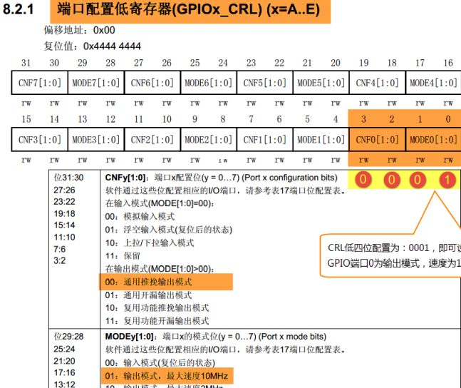
Configure the GPIO pin PB0 connected to the LED lamp to the output mode, that is, configure the GPIO port to configure the low register CRL, and configure PB0 to the general push-pull output
GPIOB_CRL &= 0xFF0FFFFF;// Clear the port bit of control PB0
GPIOB_CRL |= (1<<4*0);// Configure PB0 as universal push-pull output
In the code, we first clear the port bit of the control PB0 to 0, and then assign "0001 b" to it, so as to set the GPIOB0 pin to the output mode with a speed of 10M. "& = ~" and "| =" are used in the code to avoid affecting other bits in the register, because the register cannot be read and written by bit. If we directly assign a value to the CRL register: 1 GPIOB_CRL = 0x0000001;
At this time, the lower 4 bits of CRL are set to "0001" output mode, but there is a problem with other GPIO pins, because the MODER bits of other pins have been set to input mode.
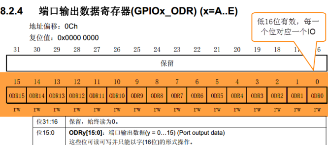
2. Control pin output level
In the output mode, write parameters to the port bit set / clear register BSRR register, port bit clear register BRR and ODR register to control the level state of the pin. The operation of BSRR and BRR ultimately affects the ODR register, and then control the GPIO through the output of the ODR register.
GPIOB_ODR &= ~(1<<0);// PB0 output low level
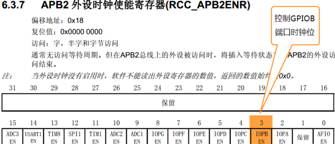
3. Turn on the peripheral clock
STM32 has many peripherals. In order to reduce power consumption, each peripheral corresponds to a clock. These clocks are turned off when the chip is just powered on. If you want the peripherals to work, you must turn on the corresponding clock. The clocks of all peripherals of STM32 are managed by a special peripheral, called RCC.
RCC_APB2ENR |= (1<<3);// Turn on GPIOB port clock
2, Programming implementation
1.c language
#include "stm32f10x.h"
#define RCC_APB2ENR		*((unsigned volatile int*)0x40021018)
#define GPIOA_CRL		*((unsigned volatile int*)0x40010800)
#define	GPIOA_ODR		*((unsigned volatile int*)0x4001080C)
#define GPIOB_CRL		*((unsigned volatile int*)0x40010C00)
#define	GPIOB_ODR		*((unsigned volatile int*)0x40010C0C)
#define GPIOC_CRH		*((unsigned volatile int*)0x40011004)
#define	GPIOC_ODR		*((unsigned volatile int*)0x4001100C)
 void Delay()
 {
   u32 i=0;
   for(;i<5000000;i++);
 }
 int main(void)
 {
	RCC_APB2ENR|=1<<2|1<<3|1<<4;
	GPIOA_CRL&=0xFFF0FFFF;
	GPIOA_CRL|=0x00020000;
	GPIOA_ODR&=~(1<<4);
	GPIOB_CRL&=0xFF0FFFFF;
	GPIOB_CRL|=0x00200000;
	GPIOB_ODR&=~(1<<5);
	GPIOC_CRH&=0xF0FFFFFF;
	GPIOC_CRH|=0x02000000;
	GPIOC_ODR&=~(1<<14);
	while(1){
		GPIOA_ODR|=1<<4;
	 	Delay();
		GPIOA_ODR&=~(1<<4);
		GPIOB_ODR|=1<<5;
	 	Delay();
		GPIOB_ODR&=~(1<<5);
		GPIOC_ODR|=1<<14;
	 	Delay();
		GPIOC_ODR&=~(1<<14);
		}
}
2. Assembly language
 AREA MYDATA, DATA

 AREA MYCODE, CODE
	ENTRY
	EXPORT led

led
    ldr r0, =0x40021018
    ldr r1, =0x0000001c
    str r1, [r0]

	ldr r0, =0x40010800
    ldr r1, [r0]
    bic r1, r1, #0x000f0000
    orr r1, r1, #0x00010000
    str r1, [r0]

    ldr r0, =0x40010c00
    ldr r1, [r0]
    bic r1, r1, #0x00f00000
    orr r1, r1, #0x00100000
    str r1, [r0]

	ldr r0, =0x40011004
    ldr r1, [r0]
    bic r1, r1, #0x0f000000
    orr r1, r1, #0x01000000
    str r1, [r0]

	ldr r0, =0x4001080c
    ldr r1, =0x00000010
    str r1, [r0]

	ldr r0, =5000000;
    ldr r1, =0

blink
    add r1, r1, #1
    cmp r1, r0
    blt blink

	ldr r1, =0x4001080c
    ldr r2, [r1]
    eor r2, r2, #0x00000010
    str r2, [r1]

	ldr r1, =0x40010c0c
    ldr r2, [r1]
    eor r2, r2, #0x00000020
    str r2, [r1]

	ldr r1, =0

blink1
	add r1, r1, #1
    cmp r1, r0
    blt blink1

	ldr r1, =0x40010c0c
    ldr r2, [r1]
    eor r2, r2, #0x00000020
    str r2, [r1]

	ldr r1, =0x4001100c
    ldr r2, [r1]
    eor r2, r2, #0x00004000
    str r2, [r1]

	ldr r1, =0

blink2
	add r1, r1, #1
    cmp r1, r0
    blt blink2

	ldr r1, =0x4001100c
    ldr r2, [r1]
    eor r2, r2, #0x00004000
    str r2, [r1]

	ldr r1, =0x4001080c
    ldr r2, [r1]
    eor r2, r2, #0x00000010
    str r2, [r1]

	ldr r1, =0
    b blink

	END
3. Realization
Waveform display:
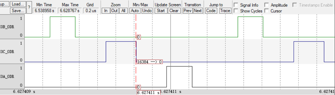
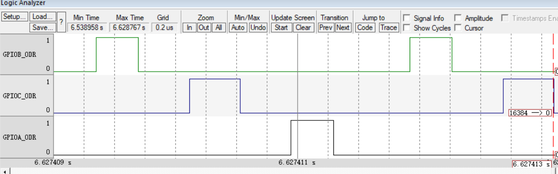
The interval difference is 0.000002s, which is exactly 1s after conversion
3, Summary
Learn and understand the principles of address mapping and register mapping of STM32F103 series chips; Understand the three steps of GPIO port initialization setting (clock configuration, input / output mode setting and maximum rate setting).