1, Experimental principle
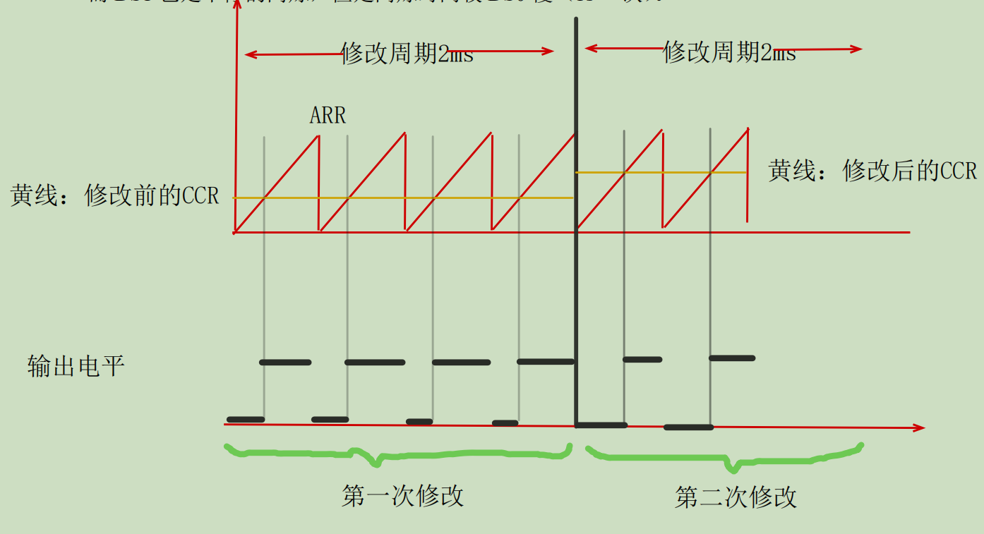
Analysis: the clock is 84Mhz, the frequency is 84, the ARR is set to 500, the clock obtained by the counter is 84M/84=1 Mhz, and the counting time is 0.5ms In the main function, the modification time I set is 2ms once. As shown in the figure, set PWM1 mode, and the output polarity low level is valid. That is, when the count value is less than the comparison value, the low level is output. Before modification, the value of CCR is relatively small and the time of outputting low level is short. In 2ms, the average voltage obtained is small and the brightness of LED is dark. Modify the value of CCR, so that the output time of low level is long, the average voltage of LED is high, and the light brightness becomes bright. And so on. Modify the value every 2ms, and the proportion of low level becomes higher and higher until it is equal to arr and reaches the brightest state. Then it decreases, and then the brightness gradually darkens, which goes back and forth to achieve the effect of breathing lamp.
2, Program configuration analysis
Step 1: enable the clock of timer 14 and the clock of GPIO port
RCC_APB1PeriphClockCmd(RCC_APB1Periph_TIM14,ENABLE);  	//Start timer TIM14 clock
RCC_AHB1PeriphClockCmd(RCC_AHB1Periph_GPIOF, ENABLE); 	//To enable the clock of GPIOF, the clock must be enabled to use an IO port
//Not as an ordinary pin, but as a pin of timer peripheral
GPIO_PinAFConfig(GPIOF,GPIO_PinSource9,GPIO_AF_TIM14); //GPIOF9 is multiplexed into timer 14
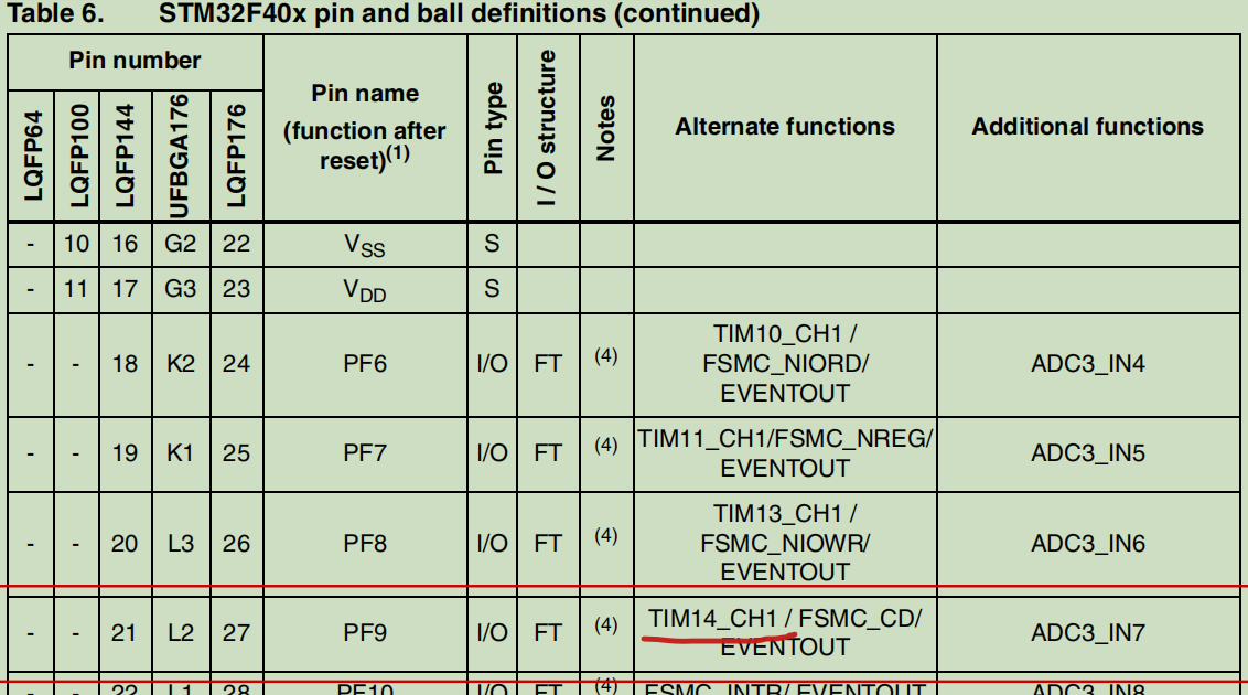
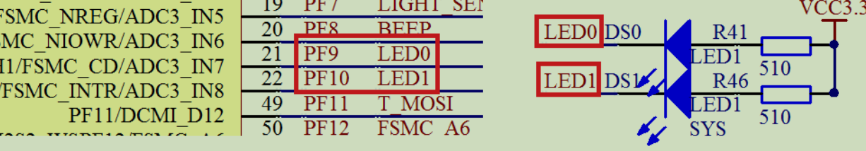
Analysis: first of all, the purpose of the experiment is to use PWM to control the brightness of LED. Here we choose the on-time F407 development board, and the pin corresponding to LED0 (red light) is PF9. It can be seen from the chip manual that PF9 can be used as the output of CH1 channel of timer 14. Therefore, timer 14 is selected here. Of course, we want to turn on the clock of GPIOF and timer 14.
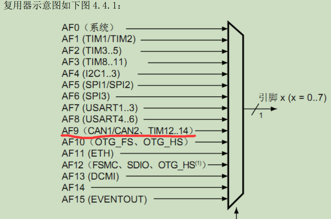
In addition, PF9 here is no longer used as an ordinary input / output I/O port, but as a built-in peripheral port of timer 14. Port multiplexing is naturally used, that is, GPIOF9 port is multiplexed into the port of timer 14.
Supplementary port reuse concept:
    //Initialize GPIOF9
	GPIO_InitStructure.GPIO_Pin = GPIO_Pin_9;           //GPIOF9
	GPIO_InitStructure.GPIO_Mode = GPIO_Mode_AF;        //Reuse function
	GPIO_InitStructure.GPIO_Speed = GPIO_Speed_100MHz;	//Speed 100MHz
	GPIO_InitStructure.GPIO_OType = GPIO_OType_PP;      //Push pull multiplex output
	GPIO_InitStructure.GPIO_PuPd = GPIO_PuPd_UP;        //Pull up
	GPIO_Init(GPIOF,&GPIO_InitStructure);               //Initialize PF9
Analysis: first select the initialization pin, here select PF9, then set it as multiplexing function and set the output speed of I/O port
Here, the key is to set the pull-up
    //Initialization timer
	TIM_TimeBaseStructure.TIM_Prescaler=psc;  //Timer frequency division
	TIM_TimeBaseStructure.TIM_CounterMode=TIM_CounterMode_Up; //Count up mode
	TIM_TimeBaseStructure.TIM_Period=arr;   //Automatic reload value
	TIM_TimeBaseStructure.TIM_ClockDivision=TIM_CKD_DIV1;//Clock division
	TIM_TimeBaseInit(TIM14,&TIM_TimeBaseStructure);//Initialization timer 14
Analysis: after turning on the clock of TIM14, we need to set the values of ARR and PSC registers to control the output PWM
	//Initialize TIM14 Channel1 PWM mode
	TIM_OCInitStructure.TIM_OCMode = TIM_OCMode_PWM1; //Select timer mode: TIM pulse width modulation mode 1
 	TIM_OCInitStructure.TIM_OutputState = TIM_OutputState_Enable; //Compare output enable CCER
	TIM_OCInitStructure.TIM_OCPolarity = TIM_OCPolarity_Low; //Output polarity: the polarity of TIM output is relatively low
	TIM_OC1Init(TIM14, &TIM_OCInitStructure);  //Initialize the peripheral TIM1 4OC1 according to the parameters specified by T
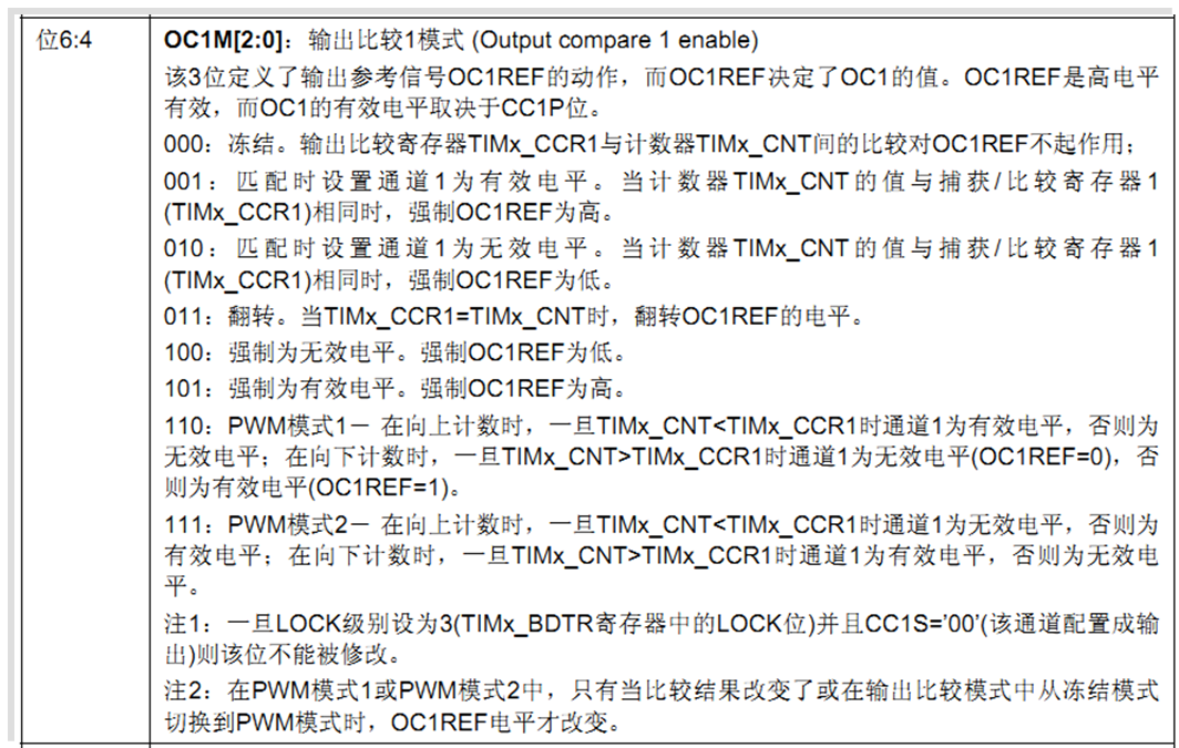
Analysis: setting tim14_ When we configure CCR1 to be low, we want DS0 to be on by default, because when we configure CCR1 to be low, we want DS0 to be on by default_ The correlation bit of ccmr1 controls TIM14_CH1 mode. In the library function, the PWM channel is set through the function TIM_OC1Init()~TIM_OC4Init(). The setting functions of different channels are different. Here we use channel 1, so the function used is TIM_OC1Init().
The first parameter: set whether the mode is PWM or output comparison. Here, when we are in PWM1 mode, when counting up
When the timer value is less than the set value of the comparator, the TIMX output pin outputs the effective potential at this time.
When the timer value is greater than or equal to the set value of the comparator, the TIMX output pin outputs an invalid potential at this time.
At this time, the level of the output is still uncertain, but whether the output is valid when it is lower or higher than the comparison value CCR1 is set.
Second parameter: CCER:CC1E bit: input / capture 1 output enable. 0: off, 1: on. To output PWM from IO port, this bit must be set to 1
The third parameter: whether the specific output is high level or low level, tim14 should be set_ CCER:CC1P bit in CCER register: input / capture 1 output polarity. 0: active at high level, 1: active at low level.
Initialize the structure according to the above parameters
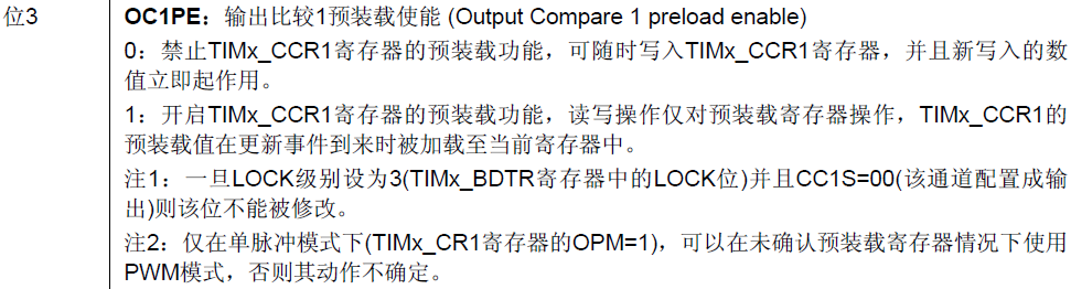
Step 5: enable the preload register of TIM14 on CCR1
TIM_OC1PreloadConfig(TIM14, TIM_OCPreload_Enable); //Enable TIM14 preload register on CCR1
Analysis: there are two capture / comparison registers of four channels, the preload register and shadow register of CCRx. There are two ways to transfer from the preload register of CCRx to the shadow register: one is to execute the new comparison value immediately after modification, and the other is to change the comparison value in the next cycle. This function is used to set how to update the comparison value CCR1
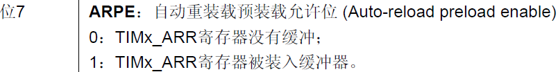
Step 6: ARPE enable
TIM_ARRPreloadConfig(TIM14,ENABLE);//ARPE enable
Analysis: the main function is to transfer the ARR preload register to the shadow register. This function determines how to modify the ARR, that is, the set count value TIM_ The arrreloadconfig function modifies the CR1 - > APRE bit according to timx_ Setting of APRE bit in CR1 register: when APRE=0, the contents of the preloaded register can be transferred to the shadow register at any time. At this time, the two are connected; When APRE=1, the contents of the preload register (ARR) are transferred to the shadow register only at each update event (UEV). See the following for details: http://t.csdn.cn/6U3Mh
Step 7: enable TIM14. After the configuration is ready, you have to turn on the switch, which is equivalent to the decoration of the home. Now you have to open the door to receive guests.
TIM_Cmd(TIM14, ENABLE); //Enable TIM14
---------------------------------------------------------------------------------------------------------------------------------
Complete code
---------------------------------------------------------------------------------------------------------------------------------
Initialization code:
void TIM14_PWM_Init(u32 arr,u32 psc)
{
	//In this part, you need to manually modify the IO port settings

	GPIO_InitTypeDef GPIO_InitStructure;
	TIM_TimeBaseInitTypeDef  TIM_TimeBaseStructure;
	TIM_OCInitTypeDef  TIM_OCInitStructure;

	RCC_APB1PeriphClockCmd(RCC_APB1Periph_TIM14,ENABLE);  	//Start timer TIM14 clock
	RCC_AHB1PeriphClockCmd(RCC_AHB1Periph_GPIOF, ENABLE); 	//To enable the clock of GPIOF, the clock must be enabled to use an IO port
	//Not as an ordinary pin, but as a pin of timer peripheral
	GPIO_PinAFConfig(GPIOF,GPIO_PinSource9,GPIO_AF_TIM14); //GPIOF9 is multiplexed into timer 14
	//Initialize GPIOF9
	GPIO_InitStructure.GPIO_Pin = GPIO_Pin_9;           //GPIOF9
	GPIO_InitStructure.GPIO_Mode = GPIO_Mode_AF;        //Reuse function
	GPIO_InitStructure.GPIO_Speed = GPIO_Speed_100MHz;	//Speed 100MHz
	GPIO_InitStructure.GPIO_OType = GPIO_OType_PP;      //Push pull multiplex output
	GPIO_InitStructure.GPIO_PuPd = GPIO_PuPd_UP;        //Pull up
	GPIO_Init(GPIOF,&GPIO_InitStructure);              //Initialize PF9
	//Initialization timer
	TIM_TimeBaseStructure.TIM_Prescaler=psc;  //Timer frequency division
	TIM_TimeBaseStructure.TIM_CounterMode=TIM_CounterMode_Up; //Count up mode
	TIM_TimeBaseStructure.TIM_Period=arr;   //Automatic reload value
	TIM_TimeBaseStructure.TIM_ClockDivision=TIM_CKD_DIV1;//Clock division
	TIM_TimeBaseInit(TIM14,&TIM_TimeBaseStructure);//Initialization timer 14

	//Initialize TIM14 Channel1 PWM mode
	TIM_OCInitStructure.TIM_OCMode = TIM_OCMode_PWM1;  //TIM14_CCRM1_OCM1[2:0] Select timer mode: Tim pulse width modulation mode 1
 	TIM_OCInitStructure.TIM_OutputState = TIM_OutputState_Enable; //TIM14_CC1E_ Compare output enable
	TIM_OCInitStructure.TIM_OCPolarity = TIM_OCPolarity_Low; //TIM14_CCER_CC1P output polarity: Tim output polarity is relatively low
	TIM_OC1Init(TIM14, &TIM_OCInitStructure);  //Initialize the peripheral TIM1 4OC1 according to the parameters specified by T

	TIM_OC1PreloadConfig(TIM14, TIM_OCPreload_Enable);  //TIM14_CCRM1_OC1P1 enables the preload register of tim14 on CCR1

     TIM_ARRPreloadConfig(TIM14,ENABLE);//ARPE enable -- TIMx_CR1_ARPE register

	TIM_Cmd(TIM14, ENABLE);  //Enable TIM14---TIMx_CR1_CEN register


}
Main function code:
int main(void)
{
	u16 led0pwmval=0;
	u8 dir=1;
	//NVIC_PriorityGroupConfig(NVIC_PriorityGroup_2);// Set system interrupt priority group 2
	delay_init(168);  //Initialization delay function
	//uart_init(115200);// The baud rate of initialization serial port is 115200
 	TIM14_PWM_Init(500-1,84-1);	//84M/84=1Mhz counting frequency, reloading value 500, so PWM frequency is 1M/500=2Khz
   while(1) //The comparison value is incremented from 0-300 to 300 and then decremented from 300-0
	{
 		delay_ms(2);	 //It's really not good without delay
		if(dir) led0pwmval++;//dir==1 led0pwmval increment
		else led0pwmval--;	//dir==0 led0pwmval decrement
 		if(led0pwmval>300)dir=0;//When led0pwmval reaches 300, the direction is decreasing
		if(led0pwmval==0)dir=1;	//When led0pwmval decreases to 0, the direction changes to increase

		TIM_SetCompare1(TIM14,led0pwmval);	//Modify the comparison value and duty cycle
	}
}