when the STM8 single chip microcomputer uses the ADC function to read the values of multiple channels, it can use the single mode. After sampling one channel, reinitialize the other channel, and then sample. After sampling, continue to reinitialize and switch to the next channel. But this sampling is too troublesome. STM8 single chip microcomputer provides a scanning mode, which can sample the values of multiple channels in sequence. After all the channels are sampled, the flag bit will be set, so that the values of multiple channels can be read out at one time.
The official documents are as follows:
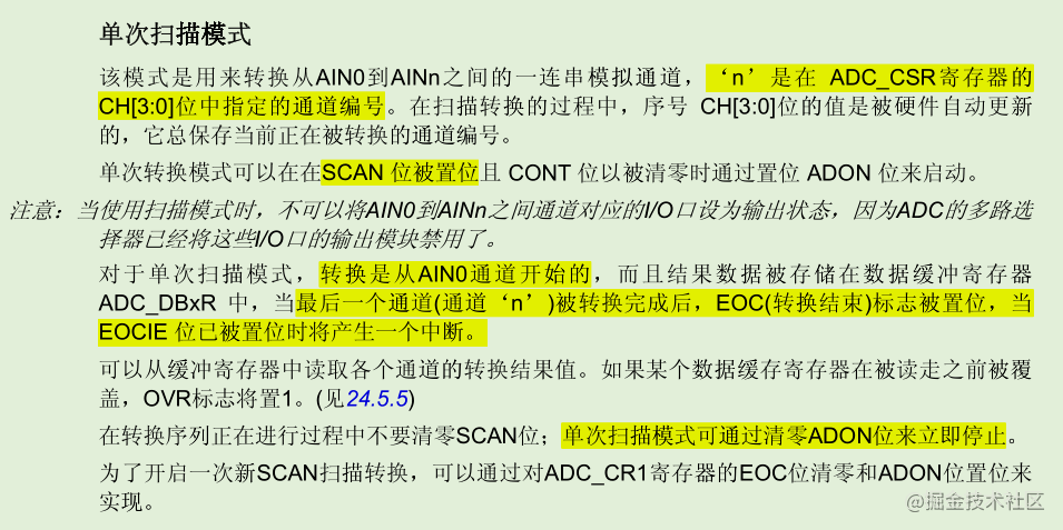
as can be seen from the document, the sampling starts from channel 0. For example, if you want to sample three channel values, the sampling channel number is 0-3. If you want to sample channels 3 and 4, you have to start from channel 0, that is, you have to scan from channel 0 to channel 4. Even if channels 0, 1 and 2 are not used, it will scan. This is not good.
ADC during single sampling_ The channel number in CSR register refers to the channel number to be sampled. The channel to be sampled is set to. In scanning mode, this channel number refers to the maximum channel number to be scanned. Scanning starts from channel 0. Pay attention when setting here.
the configuration of single scan mode is actually very simple, but there is one more setting to enable scanning than single scan mode. Next, the setting method of single scan mode is described directly through the register.
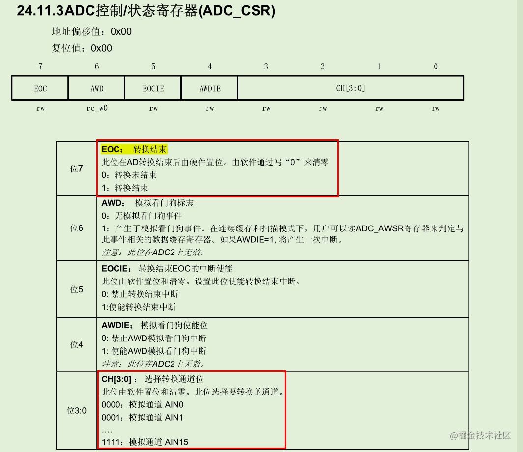
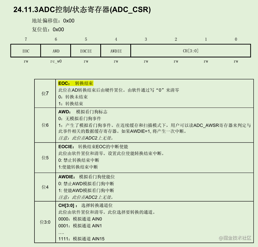
first look at ADC_CSR register. Only one channel conversion bit needs to be set in this register. This channel refers to the maximum channel scanned. In single mode, this channel refers to the channel value to be read, while in scan mode, this channel refers to the maximum number of scan channels. Scanning starts from channel 0. EOC bit is the end of conversion flag bit, which does not need to be set during initialization, but the channel judges this bit to read when reading data.
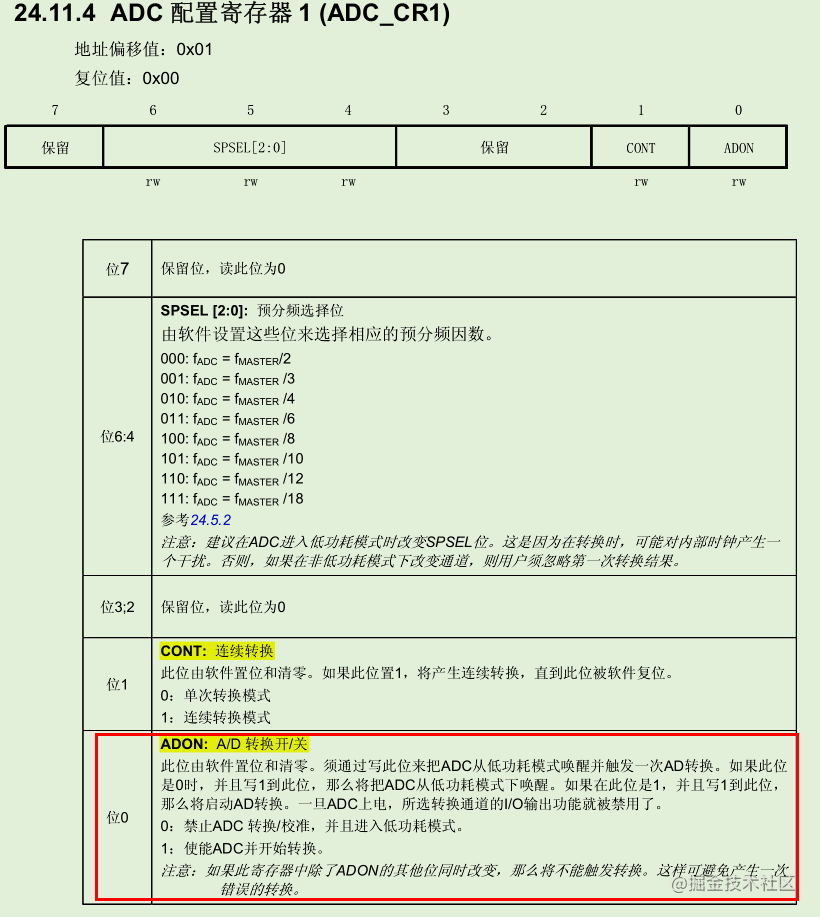
next, look at ADC_CR1 register, the only one to be set in this register is the ADON bit, which is used to control the conversion switch of ADC. When it is 1, the conversion function is started and when it is 0, the conversion function is closed. The default values of pre frequency division bit and single conversion mode are 0, which just meets our needs, that is, the default 2 frequency division and single conversion mode.
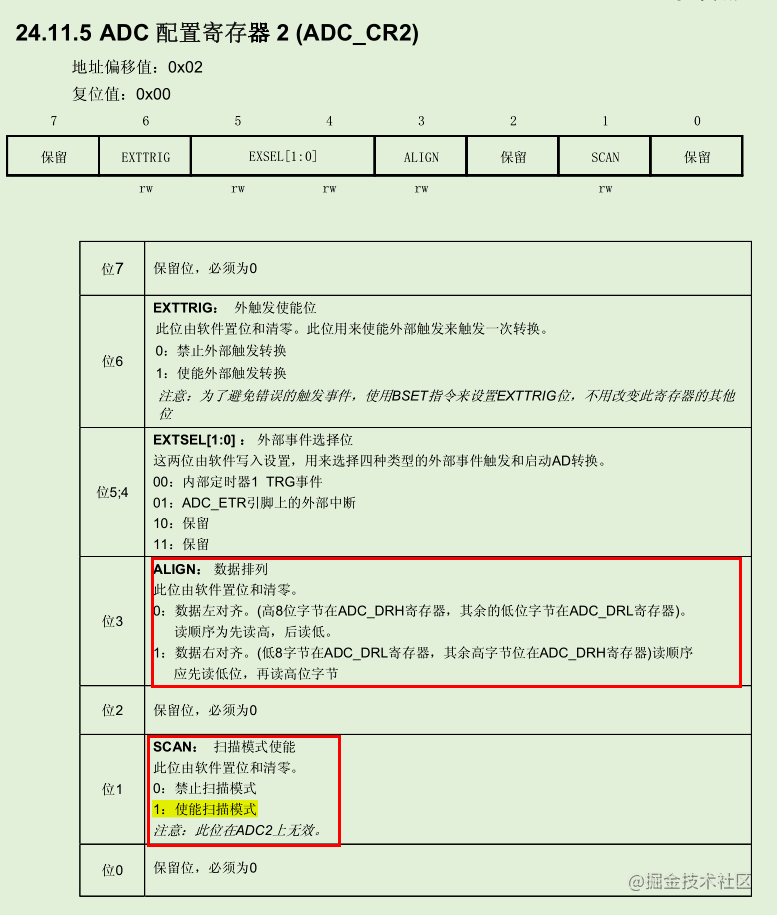
next, look at ADC_CR2 register. In fact, there is only one bit that must be set in this register, that is, to use the SCAN mode, you must set the SCAN bit to 1, and use the default value for other bits. If the data alignment uses left alignment, you don't need to set it. The right alignment of data is used here, so it is necessary to set the ALIGN bit to 1 Other bits default to 0
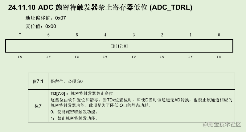
finally, this ADC_TDR register, used to prohibit Schmitt trigger, is mainly used to reduce the power consumption of MCU. Of course, this register can be set without setting. If you want to set which ADC channels are used, just set the corresponding channel position 1.
now you can start writing code:
#include "adc.h"
#include "main.h"
#include "led.h"

_Bool ADC_flag = 0;                     //ADC conversion success flag
u16 ADC_DB[10] = {0};
u16 adc_data[5] = {0};

//AD channel pin initialization
void ADC_GPIO_Init( void )
{
    PD_DDR &= ~( 1 << 2 );              //PD2 set as input
    PD_CR1 &= ~( 1 << 2 );              //PD2 is set as suspended input

    PD_DDR &= ~( 1 << 3 );              //PD3 set as input
    PD_CR1 &= ~( 1 << 3 );              //PD3 is set as suspended input

    PC_DDR &= ~( 1 << 4 );              //PC4 set as input
    PC_CR1 &= ~( 1 << 4 );              //PC4 is set as suspended input
}

//Set to single scan mode
//ch is the data of ADC channel continuously converting AIN0---AINch channel
void ADC_CH_Init( u8 ch )
{
    char l = 0;
    ADC_GPIO_Init();
    ADC_CR1 &= ~( 7 << 4 );   //Prescaler 2
    ADC_CR2 &= ~( 1 << 6 );   //Do not use external triggers
    //Disable the Schmitt trigger of ain2 and ain4 to reduce the static power consumption of IO. If the Schmitt mode is disabled, the serial port will not be able to send and receive data!
    ADC_TDRL |= ( 1 << 2 );
    ADC_TDRL |= ( 1 << 3 );
    ADC_TDRL |= ( 1 << 4 );

    ADC_CR1 &= ~( 1 << 1 );   //Single conversion
    ADC_CSR |= 0x04;          //Configure the one with the largest channel number
    ADC_CR2 |= ( 1 << 3 );    //Right align

    ADC_CR1 |= ( 1 << 0 );    //Turn on the ADC
    ADC_CR2 |= ( 1 << 1 );    // SCAN = 1 turns on scan mode

    //When the ADON bit is set for the first time, the ADC wakes up from the low power mode. In order to start the conversion, the ADC must be set with a write instruction a second time_ ADON bit of CR1 register.
    for( l = 0; l < 10; l++ );  //Delay to ensure that the power on of ADC module is completed for at least 7us
    ADC_CR1 |= ( 1 << 0 );      //Enable the ADC again at the lowest position 1 of the CR1 register and start the conversion
}

u16 ain2_val = 0,ain3_val = 0,ain4_val = 0;
//Read the sampling voltage value
u16 ReadVol_CHx( void )
{
    u16 voltage = 0;
    u16 temph = 0;
    u8 templ = 0;
    while( 1 )
    {
        LED = !LED;             //The program takes 15us to run for one circle
        while( ( ADC_CSR & 0x80 ) == 0 );      //Wait for the end of conversion. The waiting time is 4us
        ADC_CSR &= ~( 1 << 7 );               // The conversion end flag bit is cleared EOC

        //Read the value of AIN2
        templ = ADC_DB2RL;
        temph = ADC_DB2RH;
        temph = ( u16 )( templ | ( u16 )( temph << ( u16 )8 ) );
        ain2_val =  temph;

        //Read the value of AIN3
        templ = ADC_DB3RL;
        temph = ADC_DB3RH;
        temph = ( u16 )( templ | ( u16 )( temph << ( u16 )8 ) );
        ain3_val =  temph;

        //Read the value of AIN4
        templ = ADC_DB4RL;
        temph = ADC_DB4RH;
        temph = ( u16 )( templ | ( u16 )( temph << ( u16 )8 ) );
        ain4_val =  temph;

        ADC_CR1 |= 0x01;                        //Turn on a conversion
    }
    return voltage;
}
The initialization process is carried out according to the process analyzed above. It needs to be started twice when starting ADC conversion.
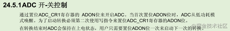
after the system is started, the ADC is in the low-power mode by default. The first time the ADON bit is set is to wake the ADC from the low-power mode, and then it needs to delay 1 conversion cycle to wait for the system conversion to be stable. Therefore, it is necessary to set ADON to 1 twice during initialization. Since the single trigger mode is used here, the ADC is turned off by default after each conversion. If you want to continue the conversion, you need to manually set the ADON bit to 1
you can also use interrupt to read data.
#include "adc.h"
#include "main.h"
#include "led.h"

_Bool ADC_flag = 0;                     //ADC conversion success flag

u16 ADC_DB[10] = {0};
u16 adc_data[5] = {0};

//AD channel pin initialization
void ADC_GPIO_Init( void )
{
    PD_DDR &= ~( 1 << 2 );              //PD2 set as input
    PD_CR1 &= ~( 1 << 2 );              //PD2 is set as suspended input

    PD_DDR &= ~( 1 << 3 );              //PD3 set as input
    PD_CR1 &= ~( 1 << 3 );              //PD3 is set as suspended input

    PC_DDR &= ~( 1 << 4 );              //PC4 set as input
    PC_CR1 &= ~( 1 << 4 );              //PC4 is set as suspended input
}

//Set to single scan mode
//ch is the data of ADC channel continuously converting AIN0---AINch channel
void ADC_CH_Init( u8 ch )
{
    char l = 0;
    ADC_GPIO_Init();

    ADC_CR1 &= ~( 7 << 4 );   //Prescaler 2
    ADC_CR2 &= ~( 1 << 6 );   //Do not use external triggers
    //Disable the Schmitt trigger of ain2 and ain4 to reduce the static power consumption of IO. If the Schmitt mode is disabled, the serial port will not be able to send and receive data!
    ADC_TDRL |= ( 1 << 2 );
    ADC_TDRL |= ( 1 << 4 );

    ADC_CR1 &= ~( 1 << 1 );   //Single conversion
    ADC_CSR |= 0x04;          //Configure the one with the largest channel number
    ADC_CR2 |= ( 1 << 3 );    //Right align

    ADC_CR1 |= ( 1 << 0 );    //Turn on the ADC
    ADC_CR2 |= ( 1 << 1 );    // SCAN = 1 turns on scan mode

    ADC_CSR |= ( 1 << 5 );    //EOCIE enable conversion end interrupt

    //When the ADON bit is set for the first time, the ADC wakes up from the low power mode. In order to start the conversion, the ADC must be set with a write instruction a second time_ ADON bit of CR1 register.
    for( l = 0; l < 10; l++ );  //Delay to ensure that the power on of ADC module is completed for at least 7us
    ADC_CR1 |= ( 1 << 0 );      //Enable the ADC again at the lowest position 1 of the CR1 register and start the conversion

}
u16 ain2_val = 0, ain3_val = 0, ain4_val = 0;
u16 temph = 0;
u8 templ = 0;
//Read the sampling voltage value
u16 ReadVol_CHx( void )
{
    u16 voltage = 0;
    if( ADC_flag == 1 )
    {
        ADC_flag = 0;
        //In single channel scanning mode, the conversion results are stored in ADC_DBxR register
        //Read the value of AIN2
        templ = ADC_DB2RL;
        temph = ADC_DB2RH;
        temph = ( u16 )( templ | ( u16 )( temph << ( u16 )8 ) );
        ain2_val =  temph;

        //Read the value of AIN3
        templ = ADC_DB3RL;
        temph = ADC_DB3RH;
        temph = ( u16 )( templ | ( u16 )( temph << ( u16 )8 ) );
        ain3_val =  temph;

        //Read the value of AIN4
        templ = ADC_DB4RL;
        temph = ADC_DB4RH;
        temph = ( u16 )( templ | ( u16 )( temph << ( u16 )8 ) );
        ain4_val =  temph;

        ADC_CR1 |= 0x01;                        //Turn on a conversion
    }
    return voltage;
}
//AD interrupt service function interrupt number 22
#Pragma vector = 24 / / for the interrupt number in IAR, add 2 to the interrupt number in STVD
__interrupt void ADC_Handle( void )
{
    ADC_CSR &= ~( 1 << 7 );               // The conversion end flag bit is cleared EOC
    ADC_flag = 1;                       // ADC interrupt flag set to 1
}
The start of the interrupt is to turn on the ADC_ The EOCIE bit of CSR register is set to 1, and then when all channel conversion is completed, an interrupt will be generated to read data in the interrupt.
it should be noted here that in the scanning mode, the sampled data results are not stored in the ADC_DR register, but stored in ADC_ In the dbxr register, the channels are stored in the corresponding ADC_ In the dbxr register, this register is divided into high-order and low-order. For example, the data of channel 2 is stored in the ADC_DB2RL and ADC_ In the db2rh register, you should also pay attention when reading data. If the data is left aligned, you must read the high 8 bits first, and then the low bits. If the data is right aligned, the lower 8 bits must be read first and the upper 8 bits must be read later.
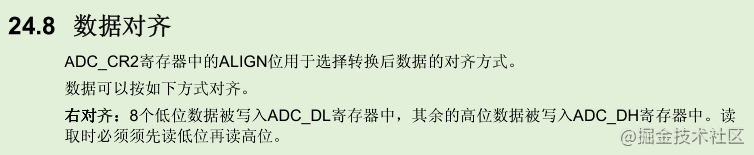
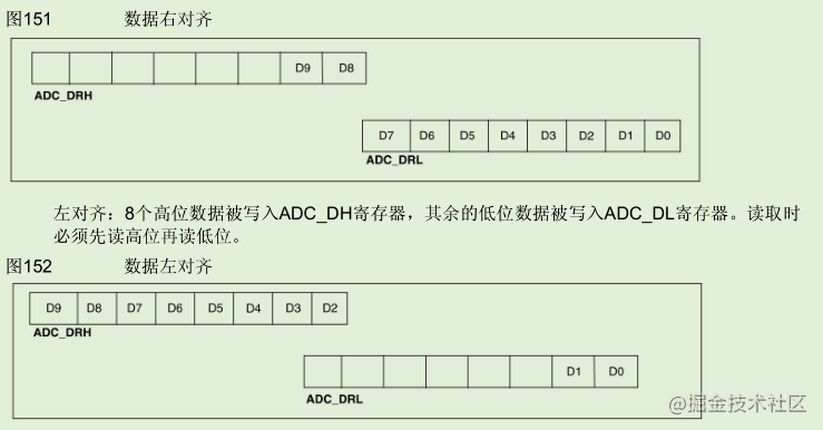
Data alignment is described in detail in the official manual, which should be paid attention to when using.