DDS
1 DDS
1.1 DDS core idea
1.1.1 phase amplitude table of sine wave:
It has a sufficiently fine phase step. N is the serial number of data, phase is the phase, Am is the calculated value of sine wave, and Data_10 is the hexadecimal representation of 10 bit digital quantity, which is described by a 10 bit DAC, in which the actual value corresponding to 512 is 0.
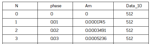
The sine wave amplitude increases from 0, but it is not represented by the DAC output until the 12th point.
The fixed clock MCLK is 36MHz, and the DAC traverses the table at the beat of MCLK. If the step is 1, then:
f
O
U
T
=
1
T
M
C
L
K
×
N
max
m
=
f
M
C
L
K
×
m
N
max
=
36
×
1
0
6
×
1
36000
=
1000
H
z
f_{O U T}=\frac{1}{T_{M C L K} \times \frac{N_{\max }}{m}}=\frac{f_{M C L K} \times m}{N_{\max }}=\frac{36 \times 10^{6} \times 1}{36000}=1000 \mathrm{~Hz}
fOUT=TMCLK×mNmax1=NmaxfMCLK×m=3600036×106×1=1000 Hz
This formula can be understood as follows: if the output sine wave traverses the whole table, it is even a cycle, and it takes 1 step to traverse
T
M
C
L
K
T_{M C L K}
TMCLK , seconds, need to go altogether
N
max
m
\frac{N_{\max }}{m}
mNmax # steps (total in the table)
N
max
N_{\max }
Nmax (two points), so that the period and frequency can be calculated.
The minimum resolution of DDS is:
Δ
f
O
U
T
=
f
M
C
L
K
×
Δ
m
N
max
=
36
×
1
0
6
×
1
36000
=
1000
H
z
\Delta f_{O U T}=\frac{f_{M C L K} \times \Delta m}{N_{\max }}=\frac{36 \times 10^{6} \times 1}{36000}=1000 \mathrm{~Hz}
ΔfOUT=NmaxfMCLK×Δm=3600036×106×1=1000 Hz
In addition, the total number of samples divided by m may not be an integer. Although the entire table cannot be completely scanned, the difference is actually very small and can be ignored.
1.1.2 kernel
It is composed of phase accumulator PA, phase amplitude meter and digital to analog converter DAC. Taking a 28 bit DAC as an example, it can count 0-
2
28
2^{28}
228. If the step length is m, the sine wave frequency is:
f
out
=
m
2
28
×
f
M
C
L
K
f_{\text {out }}=\frac{m}{2^{28}} \times f_{M C L K}
fout =228m×fMCLK
Its principle is consistent with the previous text.
The overall structure is shown in the figure:
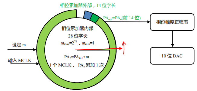
A high number of bits is generally not required outside the phase accumulator.
1.1.3 advantages and disadvantages
advantage:
- Very low frequency to very high frequency, very low frequency increment
- Fast frequency hopping
- Quadrature output, phase setting
- Sine wave, triangular wave and square wave output
Disadvantages:
- Low distortion
1.2 common chips
1.2.1 AD9833
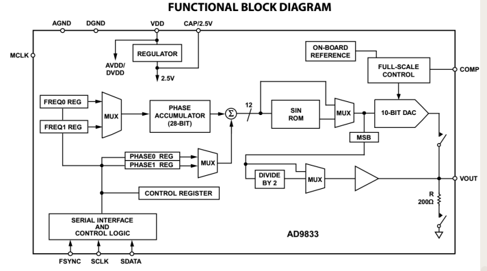
FREQ0 and FREQ1 are two frequency registers written through SPI, representing the phase step m. The two registers are designed to facilitate switching. Then there is a 28 bit phase accumulator to complete the incremental operation. The subsequent adder completes the access of phase offset, which represents the initial phase angle and exists in PHASE0 and PHASE1. The high 12 bits of the result (representing the phase) of the adder are provided to the lookup table as an address to read the content and output through the DAC.
1.3 peripheral circuit of DDS
DAC has two output modes, voltage output and complementary current output. The voltage output does not need too much processing. For example, the DAC of AD9833 is single ended current output type, which passes through the internal 200 Ω \Omega The resistance of Ω is converted into voltage output.
The current output form is generally complementary, with two pins. Take AD9850 as an example:
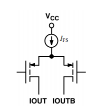
The output current of the two pins meets the following requirements:
I
O
U
T
+
I
O
U
T
B
=
I
F
S
I_{O U T}+I_{O U T B}=I_{F S}
IOUT+IOUTB=IFS
I
F
S
I_{F S}
IFS ^ is the full amplitude output current, which is controlled by
R
s
e
t
R_set
Rs # et decision. The output of the two pins can produce a differential signal with a difference of 180 °. The output is converted into voltage through resistance. Pay attention to the limit of output pin compliance voltage. The external circuit may be connected in parallel with the capacitor to play the role of low-pass filtering:
f
H
=
1
2
π
R
5
C
12
=
7.96
k
H
z
f_{H}=\frac{1}{2 \pi R_{5} C_{12}}=7.96 \mathrm{kHz}
fH=2πR5C121=7.96kHz
The sinusoidal signal should not exceed this frequency. For more effective low-pass filtering, elliptic filter can be used.
1.4 Vivado (FPGA) simulation
1.5 actual combat
1.5.1 AD9850
Structure:
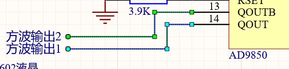
The AD9850 uses a 32-bit phase accumulator to truncate the signal into 14 bits and input it to the sinusoidal query table. The output of the query table is truncated into 10 bits and then input to the DAC, which outputs two complementary currents. The full-scale output current of DAC is adjusted by an external resistance RSET. The adjustment relationship is ISET=32(1.148V/RSET). The typical value of RSET is 3.9k Ω.
When the AD9850 is connected between the precision clock source and the written frequency and phase control word, it can generate an analog sine wave output with programmable frequency and phase. This sine wave can be directly used as a frequency signal source or converted into square wave output through an internal high-speed comparator. Under the clock of 125MHz, the 32-bit frequency control word can make the output frequency resolution of AD9850 reach 0.0291Hz; It has 5-bit phase control bits and allows the phase to be adjusted in increments of 180 °, 90 °, 45 °, 22.5 °, 11.25 ° or a combination of these values.
Control:
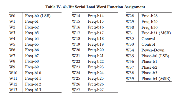
The AD9850 has a 40 bit control word, 32 bits for frequency control and 5 bits for phase control. 1 bit is used for Power down control, and 2 bits are used to select the working mode. These 40 bit control words can be input to AD9850 in parallel or serial mode. The control sequence diagram is as follows:
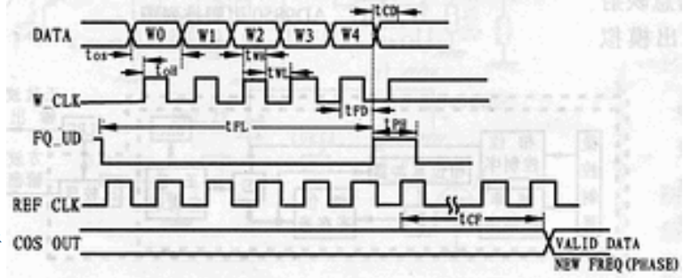
In the parallel loading mode, the data can be input to the register through the 8-bit bus. After repeating for 5 times, load the 40 bit data from the input register to the frequency / phase data register at the rising edge of FQ-UD (update the DDS output frequency and phase), and reset the address pointer to the first input register at the same time.
Load 8-bit data on the rising edge of W-CLK and point the pointer to the next input register. After five consecutive rising edges of W-CLK, the edge of W-CLK will no longer function until the reset signal or FQ-UD rising edge resets the address pointer to the first register.
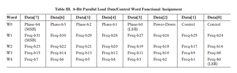
The following figure shows the meaning of each data:
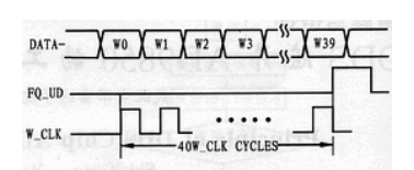
In the serial input mode, the rising edge of W-CLK moves one bit data of pin 25 in serial. After moving 40 bits, the output frequency and phase can be updated with an FQ-UD pulse. The following figure is the control sequence diagram of corresponding control word serial input:
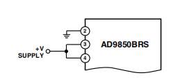
The RESET signal of AD9850 is active at high level, and the pulse width is not less than 5 reference clock cycles. The reference clock frequency of AD9850 is generally much higher than that of MCU, so the RESET end of AD9850 can be directly connected with the RESET end of MCU. The serial 3-pin and 4-pin need to be connected together:
The meanings of data representatives are as follows:
The two control bits used to select the working mode, whether parallel or serial, are best written as 00
singlechip:
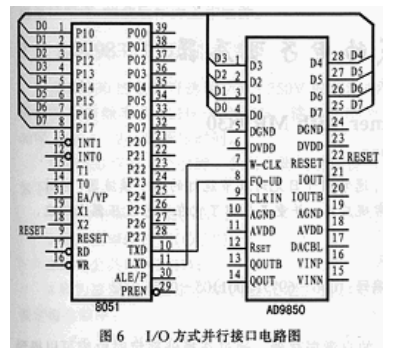
The parallel interface circuit of I/O mode is relatively simple, but it occupies relatively more resources of single chip microcomputer. The following figure is the circuit diagram of parallel interface of I/O mode. The data lines D0 ~ D7 of AD9850 are connected with P1 port, and FQ-UD and W-CLK are connected with P3 port respectively 0 (10 pin) and P3 1 (11 pin) is connected, and all timing relationships can be realized through software control.
Store DDS control words from high to low in 30H to 34H, and the assembly language is as follows:
MOV R0,#05H 		; Data 05 input R0
MOV R1,#30H  		; Data 30 input R1
DD: MOV P1,@R1 		;(30H)Incoming data on address P1,And the program location is DD
SETB P3.1 			;P3.1 Set 1
CLR P3.1 			;P3.1 Set 0
INC R1 				;R1 Data plus 1 points to the next address
DJNZ R0,DD 		;R0 Subtract 1 first. If it is not 0, it will be transferred to DD,The cycle is executed 5 times in total
SETB P3.0 			;P3.0 Set 1
CLR P3.0 			;P3.0 Set 0
END					;end
In the program, after sending a byte of data to P1 port, P3 1 (W-CLK) set high. At its rising edge, AD9850 receives the data on the data line connected to P1 port, and then sends P3 1 set low and prepare to send the next byte. After continuously sending 5 bytes, P3 0 (FQ-UD) is set high to enable AD9850 to change the frequency and phase output according to the input control word, and then set P3 0 is low, ready to send the next group. P3. Of single chip microcomputer 0,P3. Pin 1 is a serial port. When occupied, W-CLK and FQ-UD pins can also be connected with other I/O pins. At this time, it is necessary to modify the corresponding sending program.
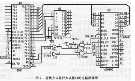
The parallel interface of bus mode occupies less MCU resources. In this mode, AD9850 only occupies a section of RAM address as an expansion chip, and only one address can be occupied when necessary. The following figure is the circuit schematic diagram of bus mode parallel interface.
Similarly, DDS control words are stored in 30H to 34H from high to low. The program list of sending control words is as follows:
MOV R0,#05H  		; Data 05 input R0
MOV R1,#30H  		; Data 30 input R1
MOV DPTR,#0700H  	; DRTR is a data pointer register, pointing to 0700h
DD: MOV A,@R1 		;(30H)Incoming data on address A,And the program location is DD
MOVX @DPTR,A		;A Incoming data DPTR Address to
INC R1 				;R1 Data plus 1 points to the next address
DJNZ R0,DD 		;R0 Subtract 1 first. If it is not 0, it will be transferred to DD,The cycle is executed 5 times in total
MOVX A,@DPTR 		;DPTR Data in the address pointed to
END					;end
The W-CLK and FQ-UD signals of AD9850 are effective on the rising edge. When the MOVX @DPTR and A command are used to transmit the control word to AD9850, the 74F138 decodes the low three bits of the high eight bit address (0700H is exactly the high eight bit address, the low three bits are the high level, and the rest are the low level), Its output is inverted (38 decoder output low effective) and combined with the inverted signal to obtain A rising edge, which is sent to the W-CLK pin of AD9850. This step is actually the key and the difference. During the execution of MOVX @DPTR and A command, WR pin becomes low level, inverts to high level, p0 outputs data, p2 outputs 8 bits higher than the address, and the output corresponding to 0700H also outputs high level after inverting through 38 decoder. After that, WCLK receives high level and controls AD9850 to receive signal. Once the program ends, WCLK receives A low level. At this time, the data sent to the bus will be received by AD9850.
After sending all the 40 bit control words for five consecutive times, use MOVA A, @ DPTR command to generate FQ-UD signal to make AD9850 change the output frequency and phase. At this time, the data read into the single chip microcomputer is actually meaningless. This step is similar to the previous one. This instruction makes the single chip microcomputer read the signal. The signal address is 0700H. Port P2 generates the high 8 bits of the signal address, and RD becomes low level. After the two phases are reversed, it becomes high level and is FQ_UD accepted; P0 accepts the signal, but the received signal is meaningless. Once the program is completed, FQ_UD received low level. The address of AD9850 in the figure is 0700H.
The above interface circuit and program are also applicable to AD9851 compatible with AD9850 pin to pin. It is worth noting that the definition of control word of AD9851 is slightly different from that of other bits in AD9850 control word, which should be paid attention to during programming.
1.5.2 schematic diagram
The schematic diagram is as follows:
The following takes AD9850 as the core and analyzes it part by part. The meaning of AD9850 pin has been given in the data manual:
D0-D7 is the 8-bit data receiving and receiving port of AD9850, which is connected to a group of IO ports of MCU:
Connect the digital power supply, digital ground, analog power supply and analog ground of AD9850 as required. The power supply is 5V:
RESET,WCLK,FQ_ The three pins of UD are led out to the row pin, which can be connected to the single chip microcomputer in the first clock mode mentioned above, and controlled by the single chip microcomputer:
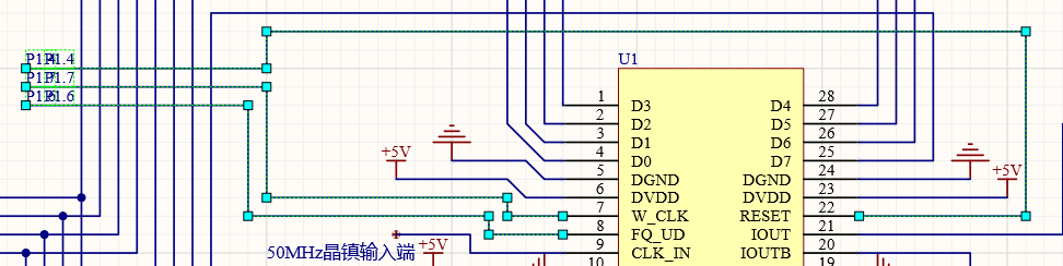
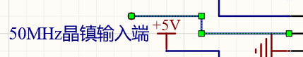
CLK_ The in pin is also led out to the row pin. It needs to be connected with a reference clock signal, and a 50MHz crystal oscillator can be connected externally (it will be turned off if it exceeds):
Two QOUT S are the outputs of the comparator, and the output is square wave. The two are complementary (AD9850 is complementary current output)
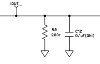
IOUT and IOUTB are complementary current outputs, and IOUT passes through 200
Ω
\Omega
The resistance of Ω is converted into voltage signal, and then the sinusoidal signal output is obtained through elliptic filter. VINP and VINN are the positive and negative input signals of the comparator. The former is directly connected to the sinusoidal output, and the latter is connected between R4 and R5 to obtain the average value of the output voltage.
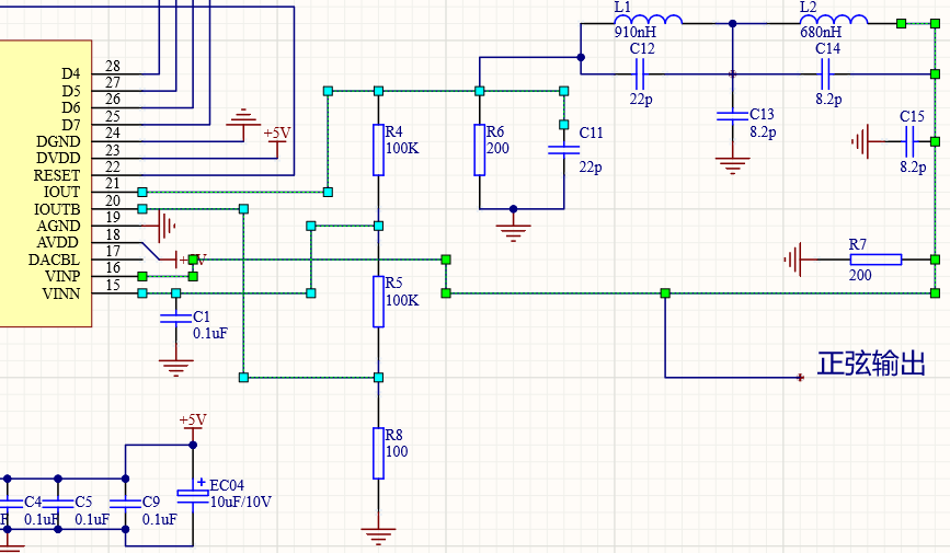
The rest will not be introduced in detail.
1.5.3 PCB and precautions
- The printed circuit board containing AD9850 shall be a multilayer board that allows dedicated power supply and ground plane
- Avoid running digital lines under equipment
- The power line to AD9850 should use the largest track possible
- Fast switching signals such as clocks shall be protected by the ground
- Avoid the intersection of digital and analog signal paths
- The analog (AVDD) and digital (DVDD) power supplies provided to the AD9850 are independent and have high-quality ceramic capacitors
1.5.4 single chip microcomputer program
/*
1 ,Step addition and subtraction of frequency output can be realized by pressing the key; Step frequency range: 0~10MHz;

2,There are six options for step values: 10Hz, 100Hz, 1000Hz, 10KHz, 100KHz and 1000KHz

3,1602 LCD screen is adopted, which can display the output frequency value in real time and the current step value. The unit of display frequency is Hz.
*/

//All basic functions are realized; two billion nine million forty-one thousand four hundred and seven
#include  <reg52. h> / / call header file (register definition inside MCU)
#define  uchar unsigned char
#define  uint unsigned int

/******This section defines the hardware I/O port********/

sbit  LCD_E  = P1^1;//Define the enable pin of 1602 LCD;
sbit  LCD_RW = P1^2;//Define the read-write pin of 1602 LCD;
sbit  LCD_RS = P1^3;//Define the gate pin of 1602 LCD;

sbit reset  = P1^4;  //Reset pin of ad9850;
sbit w_clk =  P1^7;  //Clock pin of ad9850;
sbit fqud  =  P1^6;  //Output update pin of ad9850;

#define  LCD_ Data P2 / / the port that transmits data to 1602 LCD. P2 port is used here;
#define  LCD_ Busy 0x80 / / used to detect the busy flag of LCD (delay is used in this program, not detected)
                                //LCD display content, defined to code segment;
unsigned  char code LcdBuf1[]= {"FRQ:        Hz"};
unsigned  char code LcdBuf2[]= {"Step:"};

double Con_Word_1 = 0x00;//A floating-point variable is defined to calculate the control word;
double Con_Word_2 = 0x00;//A floating-point variable is defined to calculate the control word;
long uint ConTrol_Word = 0x00;//Used to store the value of the control word;
long uint Frequency_Out;//Set frequency value;
uchar a,b,c,d,e,f,g,h; //In order to write the frequency value to 1602, first split the frequency value and store it in these eight variables;
sbit Light = P1^0; //Program status indicator, which has nothing to do with the single chip microcomputer's control of 9850, is only used when debugging the program!
//Define keys; 2X3 matrix keyboard;
sbit  P3_4 = P3^4;
sbit  P3_6 = P3^6;
sbit  P3_7 = P3^7;
sbit  P3_3 = P3^3;
sbit  P3_5 = P3^5;

uchar dat = 0;//Intermediate variables used in the process of keyboard subroutine processing;
uchar keyzhi = 0x00;//Key value; The return value of the keyboard scanning subroutine is stored in the variable;

//Function declaration
void  lcd_init(void);//1602 LCD initialization subroutine;
void  display_string(unsigned  char x,unsigned  char y,unsigned  char *s);
//Display character subroutine; x. y is the coordinate; x: The number of characters from the left: y: is it the first line or the second line;
 /**************************************************
** Function name: delay
** Entry parameter: h (unsigned int type)
** Exit parameters: None
** Function Description: short delay, using 11.0592 crystal, about 0.01MS
****************************************************/
void delay(long unsigned int h)
{
  while(h--);    //Delay subroutine
}


/**************************************************
** Function name: WriteDataLcd
** Entry parameter: wdata (unsigned char type)
** Exit: no parameters
** Function Description: write data to LCD
****************************************************/
void  WriteDataLcd(unsigned  char wdata)//Write data to 1602 LCD;
{

   LCD_RS=1;
   LCD_RW=0;
   LCD_E=0;
   LCD_E=1;
   LCD_DATA=wdata;
   delay(100);     //Short delay, instead of detecting busy state
   LCD_E=0;
}
/**************************************************
** Function name: WriteCommandLcd
** Entry parameter: wdata (unsigned char type)
** Exit parameters: None
** Function Description: write command to LCD
****************************************************/
void  WriteCommandLcd(unsigned char wdata)//Write a command to the 1602 LCD;
{

   LCD_RS=0;
   LCD_RW=0;
   LCD_E=0;
   LCD_E=1;
   LCD_DATA=wdata;
   delay(100);     //Short delay, instead of detecting busy state
   LCD_E=0;

}

//LCD initialization
void  lcd_init(void)
{
     LCD_DATA = 0;
	 delay(1000);
     WriteCommandLcd(0x38);
     delay(500);
     WriteCommandLcd(0x38); //Display mode settings
	 delay(500);
	 WriteCommandLcd(0x38); //Display mode settings
	 delay(500);
     WriteCommandLcd(0x01); //Turn off display
     WriteCommandLcd(0x38); //Display clear screen
     WriteCommandLcd(0x0c); //Display cursor movement settings
     WriteCommandLcd(0x06); //Display on and cursor movement settings
}
/**************************************************
** Function name: display_xy
** Entry parameters: x (unsigned char type), y (unsigned char type)
** Exit parameters: None
** Function Description: set the cursor position. x is the row number and y is the column number
****************************************************/
void  display_xy(unsigned  char x,unsigned  char y)
{

    if(y==0x01)
	{
     x = x + 0x40 + 0x80;
	}
	else
	{
    x = x+0x80;
	}
  WriteCommandLcd(x);
}
/*********************************************************************
** Function name: display_string
** Entry parameters: X (unsigned char), y (unsigned char), s (pointer)
** Exit parameters: None
** Function Description: display the string at the specific position, ending with / 0, x is the column number and y is the row number
**********************************************************************/
void  display_string(unsigned  char x,unsigned  char y,unsigned  char *s)
{
  display_xy(x,y);
  while(*s)
  {
   WriteDataLcd(*s);
   s++;
  }
}

Qu_Chu_Shu_Ma_Ge_Wei() //Take out each bit of data to be displayed;
 {
 		   a = Frequency_Out % 10;
 		   b = (Frequency_Out % 100)/10;
 		   c = (Frequency_Out % 1000)/100;
 		   d = (Frequency_Out % 10000)/1000;
		   e = (Frequency_Out % 100000)/10000;
		   f = (Frequency_Out % 1000000)/100000;
		   g = (Frequency_Out % 10000000)/1000000;
		   h = (Frequency_Out % 100000000)/10000000;
 }

display_data()	 //Display data subroutine
{
	Qu_Chu_Shu_Ma_Ge_Wei();//Take out each bit of data to be displayed;
	display_string(1,0,LcdBuf1);//Displays the first row, starting at position 2

	WriteCommandLcd(0x85);//If the value is displayed, use its real address, such as 0x83,
	WriteDataLcd(0x30+h); //If you want to display characters, temporarily use x and y coordinates
	WriteDataLcd(0x30+g);//The following are the data sent and displayed;
	WriteDataLcd(0x30+f);
	WriteDataLcd(0x30+e);
	WriteDataLcd(0x30+d);
	WriteDataLcd(0x30+c);
	WriteDataLcd(0x30+b);
	WriteDataLcd(0x30+a);
}

  20081207

scan_KEY(void)     //Key value processing subroutine
{
uchar key = 0;
key = P3;
key = key & 0xf8;

  switch(key)
       {
       case 0xb0:
          keyzhi = 3 ;break;
	   case 0xa8:
          keyzhi = 2 ;break;
	   case 0x98:
          keyzhi = 1 ;break;
	   case 0x70:
          keyzhi = 6 ;break;
	   case 0x68:
          keyzhi = 5 ;break;
       case 0x58:
          keyzhi = 4 ;break;
       default:
              keyzhi=0;
      }
      return(keyzhi);
}


keychuli()//Keyboard scanning subroutine
      {

		P3_3 = 0x01;P3_5 = 0x01;
		P3_4 = 0x01;P3_6 = 0x00;P3_7 = 0x00;

		delay(100);

	    if((P3_3&P3_4&P3_5) == 0x00)
		 {

		 if((P3_3&P3_4&P3_5) == 0x00)
		  {
		  P3_6 = 0x00;P3_7 = 0x01;
		  dat = scan_KEY();
		  if(dat == 0x00)
		  {
		  P3_6 = 0x01;P3_7 = 0x00;
		  dat = scan_KEY();
		  }
		  }
		  else
		  {
		  dat = 0x00;
		  goto down;//No key press
		   }
		 }

	down:return(dat);
    	}

Calculate_Control_Word(long uint Frequency_Out)
 {

  Con_Word_1 = Frequency_Out * 85;
  Con_Word_2 = Frequency_Out *0.88423027547;//50MHz calculation method
  //Firstly, the active crystal is 50MHz, then it is obtained by subtracting 1 to the 32nd power of 2 and dividing by 50MHz;

  Con_Word_2 = Con_Word_2 + 0.5;//The decimal part is rounded off;
  Con_Word_1 = Con_Word_1 + Con_Word_2;
                            //Calculate the control word in floating-point form according to the set frequency
  ConTrol_Word = Con_Word_1 / 1;//Convert control word to integer form

 }

  Send_Control_Word(long uint ConTrol_Word)//Send frequency control word to AD9850;

{
  long uint ConTrol_Word_Temporary ;
  uchar data_word ;
  w_clk = 0x00;	//According to the sequence diagram
  fqud = 0x00;  //According to the sequence diagram

  //data_word = 0x00; 	 // Set AD9851 phase, power down and other related control words
  data_word = 0x00;	 //Set AD9850 phase, power down and other related control words

  P2 = data_word;
  delay(200);
  w_clk=1;
  delay(200);
  w_clk=0;

  ConTrol_Word_Temporary = ConTrol_Word;
  ConTrol_Word = ConTrol_Word >> 24;
  data_word = ConTrol_Word % 256;//Take out W1, the highest byte in the frequency control word;

  P2 = data_word;
  delay(200);
  w_clk=1;
  delay(200);
  w_clk=0;
  ConTrol_Word = ConTrol_Word_Temporary;

  ConTrol_Word = ConTrol_Word >> 16;
  data_word = ConTrol_Word % 256;//Take out W2, the next highest byte in the frequency control word;

  P2 = data_word;
  delay(200);
  w_clk=1;
  delay(200);
  w_clk=0;
  ConTrol_Word = ConTrol_Word_Temporary;

  ConTrol_Word = ConTrol_Word >> 8;
  data_word = ConTrol_Word % 256;//Take out W3, the third byte in the frequency control word;

  P2 = data_word;
  delay(200);
  w_clk=1;
  delay(200);
  w_clk=0;
  ConTrol_Word = ConTrol_Word_Temporary;
  data_word = ConTrol_Word % 256;//Take out W4, the last byte in the frequency control word;

  P2 = data_word;
  delay(200);
  w_clk=1;
  delay(200);
  w_clk=0;	   //According to the sequence diagram
  fqud=1;	   //According to the sequence diagram
}

/************Main program**************/
main()
{
  unsigned char i = 0x00;
  uint Step_Bian_Liang = 0x00;//Step variable;
  long uint Step_Data = 10;//The default is 10Hz;
  long unsigned int Step_Data_Xian_Shi = 0x00;

  reset  =  1;	   //Reset AD9850;
  delay(1000);
  reset  =  0;	   //Put AD9850 into normal working state;

  lcd_init();	   //Initialization subroutine;

  Frequency_Out = 0;//The default frequency output value of startup is 0;
  Calculate_Control_Word(Frequency_Out);//Convert to the integer value to be sent into AD9850 according to the set frequency;
  Send_Control_Word(ConTrol_Word);      //Send frequency control word to AD9850;
  display_data();		//Display data;
  display_string(0,1,LcdBuf2);  //Display the second line, starting from position 0;

  WriteCommandLcd(0xc5);//Display data from the sixth in the second line;
  WriteDataLcd(0x30+(Step_Data/1000));//Send out display data;
  WriteDataLcd(0x30+(Step_Data/100)%10);//Send out display data;
  WriteDataLcd(0x30+(Step_Data/10)%10);//Send out display data;
  WriteDataLcd(0x30+(Step_Data%10));//Send out display data;
  display_string(9,1,"Hz");//Display Hz;

  while(1)
  {
	 keychuli();//Key processing subroutine

  if(dat == 0x01)//The key value is 1; Step plus
  {
  dat = 0x00;delay(5000);

  Frequency_Out = Frequency_Out + Step_Data;

  if(Frequency_Out > 10000000)
  {
  Frequency_Out = Frequency_Out - Step_Data;
  }
  Light =~Light;

  display_data();

  reset  =  1;	   //Reset AD9850;
  delay(100);
  reset  =  0;	   //Put AD9850 into normal working state;

  Calculate_Control_Word(Frequency_Out);//Convert to the integer value to be sent into AD9850 according to the set frequency;
  Send_Control_Word(ConTrol_Word);      //Send frequency control word to AD9850;
  }

    if(dat == 0x04)//The key value is 4; Step subtraction
  {
  dat = 0x00;delay(5000);

  if(Frequency_Out >= Step_Data)
  {
  Frequency_Out = Frequency_Out - Step_Data;
  }
  Light =~Light;

   display_data();

  reset  =  1;	   //Reset AD9850;
  delay(1000);
  reset  =  0;	   //Put AD9850 into normal working state;

  Calculate_Control_Word(Frequency_Out);//Convert to the integer value to be sent into AD9850 according to the set frequency;
  Send_Control_Word(ConTrol_Word);      //Send frequency control word to AD9850;

  }

  if(dat == 0x06)//Step selection; There are three options
  {
  dat = 0x00;delay(5000);Light =~Light;
 Step_Bian_Liang++;
 Step_Bian_Liang = Step_Bian_Liang%6;

   if(Step_Bian_Liang == 0x00)
 {
  Step_Data = 10;//Step 10; Change to 1
 }
   if(Step_Bian_Liang == 0x01)
 {
  Step_Data = 100;
 }
   if(Step_Bian_Liang == 0x02)
 {
  Step_Data = 1000;
 }
   if(Step_Bian_Liang == 0x03)
 {
  Step_Data = 10000;
 }
   if(Step_Bian_Liang == 0x04)
 {
  Step_Data = 100000;
 }
   if(Step_Bian_Liang == 0x05)
 {
  Step_Data = 1000000;
 }
  if(Step_Data<=1000)
   {
  WriteCommandLcd(0xc5);//Refer to similar sections above
  WriteDataLcd(0x30+(Step_Data/1000));
  WriteDataLcd(0x30+(Step_Data/100)%10);
  WriteDataLcd(0x30+(Step_Data/10)%10);
  WriteDataLcd(0x30+(Step_Data%10));
  display_string(9,1,"Hz ");
   }
   else
   {
   	Step_Data_Xian_Shi = Step_Data/1000;
    WriteCommandLcd(0xc5);//Refer to similar sections above
    WriteDataLcd(0x30+(Step_Data_Xian_Shi/1000));
    WriteDataLcd(0x30+(Step_Data_Xian_Shi/100)%10);
    WriteDataLcd(0x30+(Step_Data_Xian_Shi/10)%10);
    WriteDataLcd(0x30+(Step_Data_Xian_Shi%10));
    display_string(9,1,"kHz");
   }

  }

  }
}