I am xuetianyu, an FPGA enthusiast. My research direction is FPGA Architecture Exploration and digital IC design.
Focus on official account [integrated circuit design course], get more learning materials, and pull you into "IC design exchange group".
QQIC Design Communication Group No.: 866169462.
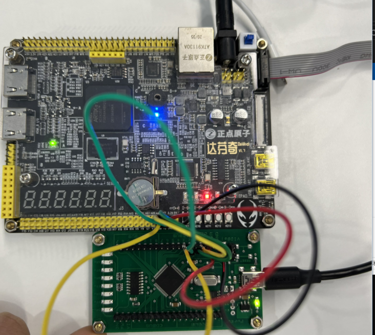
Development board used: punctual atom Da Vinci FPGA development board
Chip model: Xilinx Artix-7 35T
1, Download source code
tinyriscv official library link: https://gitee.com/liangkangnan/tinyriscv
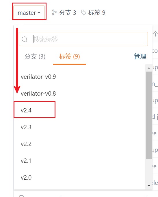
Here I choose master v2 4 version: https://gitee.com/liangkangnan/tinyriscv/tree/v2.4/
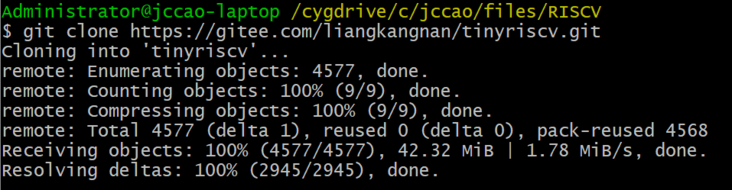
Clone locally with Git. (the terminal software used is Cygwin, installation tutorial: https://blog.csdn.net/qq_44447544/article/details/123246995?spm=1001.2014.3001.5501)
2, Create Vivado project
Open the tinyriscv folder and you can see many directories:
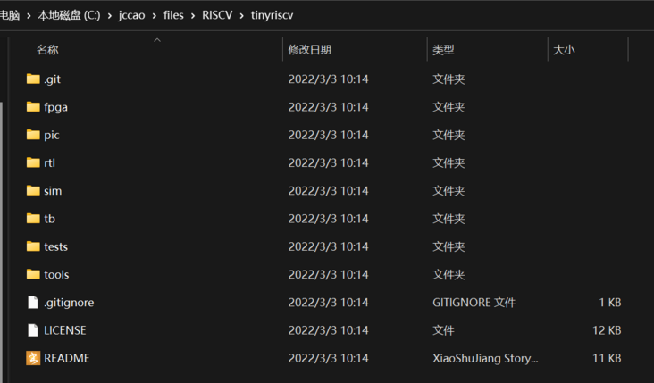
Here rtl is the source code of tinyriscv Verilog.
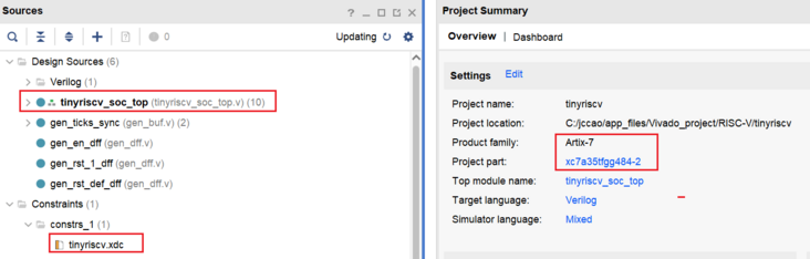
Create a project with Vivado and add the source code and constraints. See tinyriscv \ FPGA \ readme for specific steps MD file, written in great detail.
3, Modify constraint file
The so-called migration is actually to write the correct pin constraint file according to the board you use, and modify the source code according to your needs.
The basic steps are as follows:
- First modify the binding of the clock and reset pin in the constraint file
- Pin modification signal
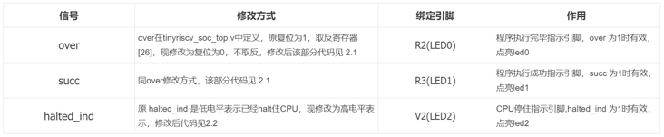
In the source code, over, succ, halted_ind is a status indication signal, which should be bound to the LED on the development board. The circuit connection mode of LED on different development boards is also different, some are on for high level and some are on for low level. In the tinyriscv source code, the low level is given, that is, when the status indication signal is valid, it is the low level, while the LED of Da Vinci development board is to light the high level, so it is necessary to modify the source code and remove it upside down.
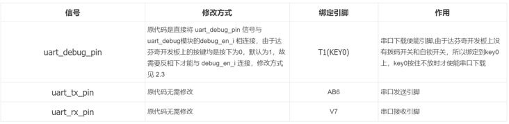
3. Modify the serial port tx and rx signal pin binding
Note: This is to bind any unused pin in the development board, not the existing serial port on the development board.
4. Modify the pin constraints used by GPIO peripherals

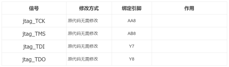
5. Modify the pin constraint used by JTAG
Note: This is to bind any unused pins in the development board, not the JTAG of FPGA. The JTAG of FPGA has been bound with the Flash on the development board and cannot be used. Like the pins bound by keys and led lights, they have been used and cannot be reused.
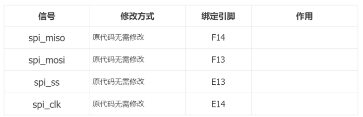
6. Modify the pin constraint used by SPI
7. Add clock constraint
Due to jtag_TCK signal is used as synchronous clock in the design, and there is no signal corresponding to crystal oscillator clock in the sensitive list. So add the following statement;
create_clock -name jtag_clk_pin -period 300 [get_ports {jtag_TCK}];
set_property CLOCK_DEDICATED_ROUTE FALSE [get_nets jtag_TCK]
Complete constraint file:
# Clock constraint 50MHz, duty cycle 50%
create_clock -add -name sys_clk_pin -period 20.00 -waveform {0 10} [get_ports {clk}];

# Clock pin
set_property -dict { PACKAGE_PIN R4 IOSTANDARD LVCMOS33 } [get_ports {clk}];

# Reset pin
set_property -dict { PACKAGE_PIN U2 IOSTANDARD LVCMOS33 } [get_ports {rst}];

# After the program is executed, the indicator pin is valid when over is 1, and led0 is lit
set_property -dict { PACKAGE_PIN R2 IOSTANDARD LVCMOS33 } [get_ports {over}];

# The program execution success indication pin is valid when succ is 1, and led1 is lit
set_property -dict { PACKAGE_PIN R3 IOSTANDARD LVCMOS33 } [get_ports {succ}];

# CPU stop indication pin, halted_ Effective when ind is 1, led2 is on
set_property -dict { PACKAGE_PIN V2 IOSTANDARD LVCMOS33 } [get_ports {halted_ind}];

# The serial port download enable pin is bound to key0 because there is no dial switch and self-locking switch. The serial port download can be enabled only when key0 is held down
set_property -dict { PACKAGE_PIN T1 IOSTANDARD LVCMOS33 } [get_ports {uart_debug_pin}];

# Serial port sending pin
set_property -dict { PACKAGE_PIN AB6 IOSTANDARD LVCMOS33 } [get_ports {uart_tx_pin}];

# Serial port receiving pin
set_property -dict { PACKAGE_PIN V7 IOSTANDARD LVCMOS33 } [get_ports {uart_rx_pin}];

# GPIO0 pin
set_property -dict { PACKAGE_PIN F16 IOSTANDARD LVCMOS33 } [get_ports {gpio[0]}];

# GPIO1 pin
set_property -dict { PACKAGE_PIN F15 IOSTANDARD LVCMOS33 } [get_ports {gpio[1]}];

# JTAG TCK pin PortA 0
set_property -dict { PACKAGE_PIN AA8 IOSTANDARD LVCMOS33 } [get_ports {jtag_TCK}];

create_clock -name jtag_clk_pin -period 300 [get_ports {jtag_TCK}];
set_property CLOCK_DEDICATED_ROUTE FALSE [get_nets jtag_TCK]


# JTAG TMS pin PortA 3
set_property -dict { PACKAGE_PIN AB8 IOSTANDARD LVCMOS33 } [get_ports jtag_TMS];

# JTAG TDI pin PortA 1
set_property -dict { PACKAGE_PIN Y7 IOSTANDARD LVCMOS33 } [get_ports {jtag_TDI}];

# JTAG TDO pin PortA 2
set_property -dict { PACKAGE_PIN Y8 IOSTANDARD LVCMOS33 } [get_ports jtag_TDO];

# SPI MISO pin
set_property -dict { PACKAGE_PIN F14 IOSTANDARD LVCMOS33 } [get_ports {spi_miso}];

# SPI MOSI pin
set_property -dict { PACKAGE_PIN F13 IOSTANDARD LVCMOS33 } [get_ports {spi_mosi}];

# SPI SS pin
set_property -dict { PACKAGE_PIN E13 IOSTANDARD LVCMOS33 } [get_ports {spi_ss}];

# SPI CLK pin
set_property -dict { PACKAGE_PIN E14 IOSTANDARD LVCMOS33 } [get_ports {spi_clk}];

#SPI related settings
set_property BITSTREAM.CONFIG.SPI_BUSWIDTH 4 [current_design]
set_property CONFIG_MODE SPIx4 [current_design]
set_property BITSTREAM.CONFIG.CONFIGRATE 50 [current_design]
set_property CFGBVS VCCO [current_design]
set_property CONFIG_VOLTAGE 3.3 [current_design]
set_property BITSTREAM.CONFIG.UNUSEDPIN PULLUP [current_design]
4, Comprehensive realization
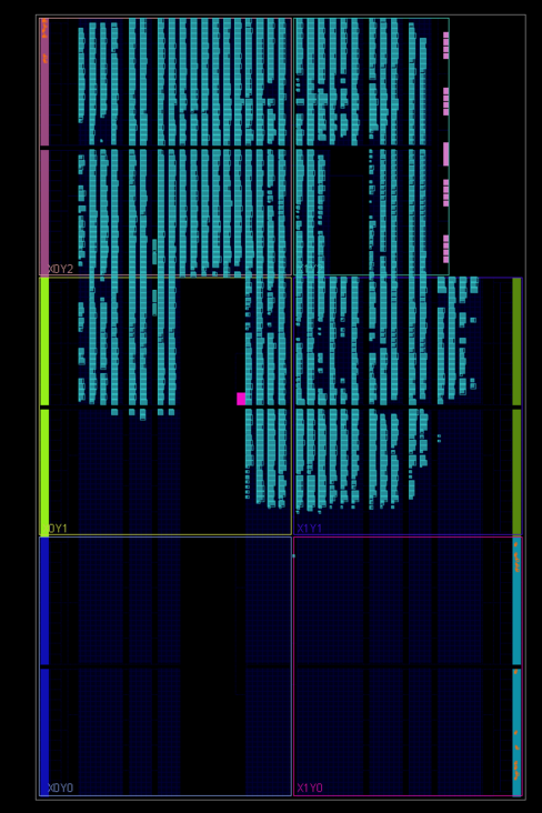
Layout:
Resource consumption;
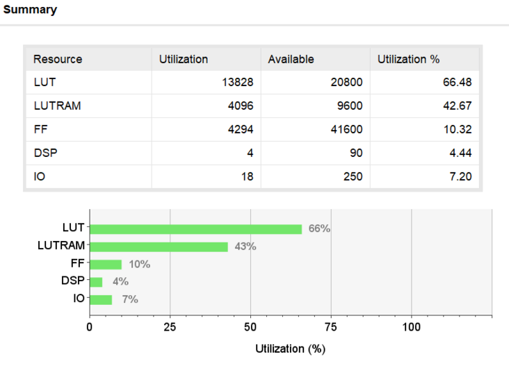
Therefore, tinyriscv can be successfully transplanted as long as the resources on the board are sufficient.
5, Through JTAG debug RISCV
Debugger chip: ftdi4232HL
Profile:
ft4232h.cfg:
adapter driver ftdi
# VID and PID
ftdi vid_pid 0x0403 0x6011
transport select jtag
# TCK frequency
adapter speed 100

# ftdi_layout_init [data] [direction]
# Specify the initial data and direction of FTDI GPIO, and 16bit data width.
# In parameter data, 1 indicates high level and 0 indicates low level, while in parameter direction, 1 indicates output and 0 indicates input (note that it is different from the conventional setting)
ftdi layout_init 0x0018 0x05fb

# ftdi_layout_signal name [-data|-ndata data_mask] [-input|-ninput input_mask] [-oe|-noe oe_mask] [-alias|-nalias name]
# Create a signal named name.
# [-data|-ndata data_mask]
# data_mask:pin mask ndata:invert -data:normal bit
# data_mask is the mask corresponding to the pin pin, - ndata indicates that the input data is reversed, - data is not reversed.

ftdi layout_signal nSRST -data 0x0010 -noe 0x0400
tinyriscv.cfg:
set _CHIPNAME riscv
jtag newtap $_CHIPNAME cpu -irlen 5 -expected-id 0x1e200a6f

set _TARGETNAME $_CHIPNAME.cpu
target create $_TARGETNAME riscv -chain-position $_TARGETNAME

riscv set_reset_timeout_sec 1

init
halt
Open cmd and execute the command: openocd - F ft4232h cfg -f tinyriscv. cfg
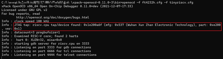
RISCV CPU detected successfully.
At present, we are learning the debug architecture of RISCV, and we will learn it later with the help of tinyriscv.
- For more technical articles and learning materials, please pay attention to my official account: integrated circuit design course.
- Unified across the platform: [snowy fish]