I. Introduction
Since November 2019, I have been learning to use HLS to realize CNN convolutional neural network and accelerate the algorithm of YOLO. But there is only the basis of image processing, no research on AI, and a little bit of HLS foundation in graduate school has long been forgotten. I hope that I can develop the habit of blogging according to the progress in the future, and record my learning and growth after work.
This post has realized the IP core of convolution operation and passed the verification of FPGA development board.
2, HLS part
For advanced comprehensive basic learning of HLS, refer to the official documents of Xilinx, ug871 vivado high level synthesis tutorial and ug902 vivado high level synthesis.
HLS realizes the convolution operation of one layer network. It uses 16bit quantization to convert the input characteristic graph and weight into 16bit fixed-point number for multiplication and addition operation. The floating-point quantification code is in the previous blog.
- TOP Function is defined as follows:
void CNN_FPGA(int *Input,int *Weight,int *Output)
Define the I / O interface as the AXI Master interface type:
#pragma HLS INTERFACE s_axilite register port=return bundle=CTRL_BUS

#pragma HLS INTERFACE s_axilite register port=Output bundle=CTRL_BUS
#pragma HLS INTERFACE m_axi depth=1024 port=Output offset=slave bundle=DATA_BUS1 num_read_outstanding=1 num_write_outstanding=1 max_read_burst_length=64 max_write_burst_length=64
#pragma HLS INTERFACE s_axilite register port=Weight bundle=CTRL_BUS
#pragma HLS INTERFACE m_axi depth=512 port=Weight offset=slave bundle=DATA_BUS2 num_read_outstanding=1 max_read_burst_length=128
#pragma HLS INTERFACE s_axilite register port=Input bundle=CTRL_BUS
#pragma HLS INTERFACE m_axi depth=1024 port=Input offset=slave bundle=DATA_BUS1 num_read_outstanding=1 num_write_outstanding=1 max_read_burst_length=64 max_write_burst_length=64
(1) . the interface protocol will map the pointer to the actual address in the DDR, read and write through the AXI Master bus. If the Axi Lite (ctrl bus) is not added, the offset address of all data is 0; after the Axi Lite bus is added, the actual offset address can be configured through the register corresponding to the offset position of the Axi Lite.
(2) . for return, the main function has no value to return, but as block level I / O protocol, Xilinx recommendations that you include the block level I / O protocol associated with the return port in the axi4 Lite interface. (ug902)
(3) About depth, I thought that depth would be mapped to FIFO or BRAM between AXI and FPGA for data storage. Later, I found that it was not. C / RTL co simulation was used to store pointer to transmit multiple read and write data at a time.
(4) . about num? Read? Outstanding: specifies how many read / write requests the AXI4 bus sets. It can be understood as the number of read-write channels.
#pragma HLS interface m_axi port=input offset=slave bundle=gmem0
depth=1024*1024*16/(512/8)
latency=100
num_read_outstanding=32
num_write_outstanding=32
max_read_burst_length=16
max_write_burst_length=16
To further improve bus efficiency, the options num_write_outstanding and num_read_outstanding ensure the design contains enough buffering to store up to 32 read and write accesses.
(4) block-level protocol
The generated IP interface protocols are AXI4 and AXI4 ﹣ Lite. You need to configure the registers in the corresponding AXI4 ﹣ Lite to determine the offset address of the data in the memory, and start the IP to work. A detailed description of each configuration register of the IP can be found in solution / impl / IP / drives. For example:
// CTRL_BUS
// 0x00 : Control signals
//        bit 0  - ap_start (Read/Write/COH)
//        bit 1  - ap_done (Read/COR)
//        bit 2  - ap_idle (Read)
//        bit 3  - ap_ready (Read)
//        bit 7  - auto_restart (Read/Write)
//        others - reserved
// 0x04 : Global Interrupt Enable Register
//        bit 0  - Global Interrupt Enable (Read/Write)
//        others - reserved
// 0x08 : IP Interrupt Enable Register (Read/Write)
//        bit 0  - Channel 0 (ap_done)
//        bit 1  - Channel 1 (ap_ready)
//        others - reserved
// 0x0c : IP Interrupt Status Register (Read/TOW)
//        bit 0  - Channel 0 (ap_done)
//        bit 1  - Channel 1 (ap_ready)
//        others - reserved
// 0x10 : Data signal of Input_r
//        bit 31~0 - Input_r[31:0] (Read/Write)
// 0x14 : reserved
// 0x18 : Data signal of Weight
//        bit 31~0 - Weight[31:0] (Read/Write)
// 0x1c : reserved
// 0x20 : Data signal of Output_r
//        bit 31~0 - Output_r[31:0] (Read/Write)
// 0x24 : reserved
// (SC = Self Clear, COR = Clear on Read, TOW = Toggle on Write, COH = Clear on Handshake)

#define XCNN_FPGA_CTRL_BUS_ADDR_AP_CTRL       0x00
#define XCNN_FPGA_CTRL_BUS_ADDR_GIE           0x04
#define XCNN_FPGA_CTRL_BUS_ADDR_IER           0x08
#define XCNN_FPGA_CTRL_BUS_ADDR_ISR           0x0c
#define XCNN_FPGA_CTRL_BUS_ADDR_INPUT_R_DATA  0x10
#define XCNN_FPGA_CTRL_BUS_BITS_INPUT_R_DATA  32
#define XCNN_FPGA_CTRL_BUS_ADDR_WEIGHT_DATA   0x18
#define XCNN_FPGA_CTRL_BUS_BITS_WEIGHT_DATA   32
#define XCNN_FPGA_CTRL_BUS_ADDR_OUTPUT_R_DATA 0x20
#define XCNN_FPGA_CTRL_BUS_BITS_OUTPUT_R_DATA 32
Among them, xcnn FPGA Ctrl bus addr AP Ctrl is the status register of the IP. You can view various status of the IP, and write 0x1 to the register, and the IP core starts to work normally.
- static definition array
Static defines arrays or other local variables, which are automatically initialized by the compiler even if they are declared unassigned. In HLS, arrays are often defined as static variables and mapped to RTL. After Reset, all arrays are initialized to 0. And the variables defined by static are saved in the global data area. Even if the function returns, its value can remain unchanged without being released.
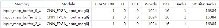
static short input_map_buffer[input_map_dimension][input_map_height][input_map_width];//8x32x32
#pragma HLS ARRAY_PARTITION variable=input_map_buffer complete dim=1
After the array is divided, only the first dimension is retained, and the second and third dimensions are completely divided.
3. memcpy function
The declaration of memcpy function in HLS is as follows:
void * __cdecl memcpy(void * __restrict__ _Dst,const void * __restrict__ _Src,size_t _Size)
Use in this design:
static int input_map_buffer_temp[input_map_length_int];
memcpy(input_map_buffer_temp,(int *)input,input_map_NUM*sizeof(int));
It should be noted that the data copied to the input ﹣ map ﹣ buffer ﹣ temp must not exceed the length of the array. The overflow data in C will not affect the data; however, in RTL, the overflow data will be re copy from the 0 address of Bram, resulting in incorrect results. Due to the different processing of this instruction by C and RTL, the project will pass the Test Bench perfectly in HLS C Simulation, but the results are quite different when the IP is generated and the board test is performed.
3, Vivado hardware connection
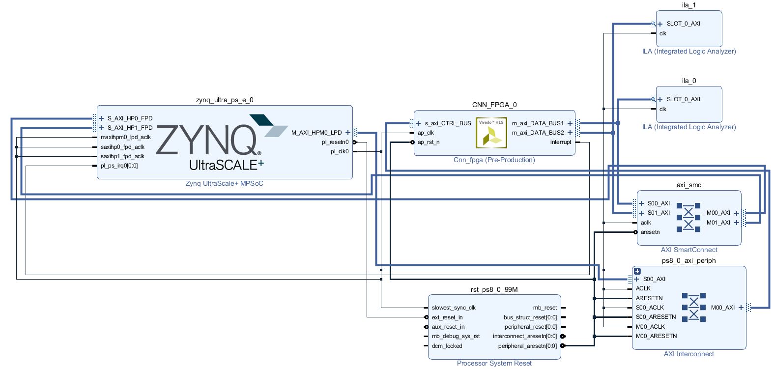
The hardware address is: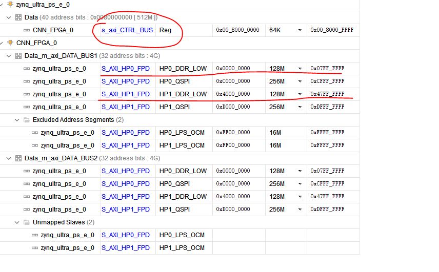
Where, the initial address of axi4 Lite corresponds to s Axi Ctrl bus; m Axi data bus1 corresponds to s Axi hp0 FPD; m Axi data bus2 corresponds to s Axi HP1 FPD;
4, PS part
This project needs to generate data source in PS test, import it into the memory address corresponding to s-axi-hp0-fpd and s-axi-hp0-fpd, and complete IP configuration and startup.
(1) Because this project runs naked, there is no system, so it is not convenient to read data files. In a stupid way:
//File: main
#include "input_map_data.h"
int main(){
...
extern const int input_map[input_map_num];
...
}
//File :input_map_data.h
const int input_map[input_map_num] = {Input test data};
(2) CPU Cache
Every time I find out the consistency between CPU and memory Cache, I slap my face again after a while. This is the most time-consuming debugging. Use memcpy or Xil out to write data to a specific address, and then start IP. The data viewed from ILA is still incorrect. After suspecting all the debugging process, I suddenly realized whether I forgot to brush the Cache and record again. Next time you write a program, don't forget
	memcpy(inupt_map_baseaddr_ptr,input_map,int_map_num*sizeof(int));

	Xil_DCacheFlush();
After writing data to memory, brush the Cache once to brush the data into memory. When reading data from memory, if DMA and other methods of data transmission have been used, the Cache in this area should be invalidated first, and then read again.
#include "xil_cache.h"
//Write something to sendram
Xil_DCacheFlushRange((u32)sendram,sizeofbuffer);//Refresh content to DDR
//Start sending DMA process....

//Start receiving DMA process.....
Xil_DCacheInvalidateRange((u32)recvram,sizeofbuffer);//Pull DDR content into Cache
//Read data from recvram!

