preface
This experiment is an ADDA test. The specific requirements, precautions and development process are as follows.
ADDA test process:
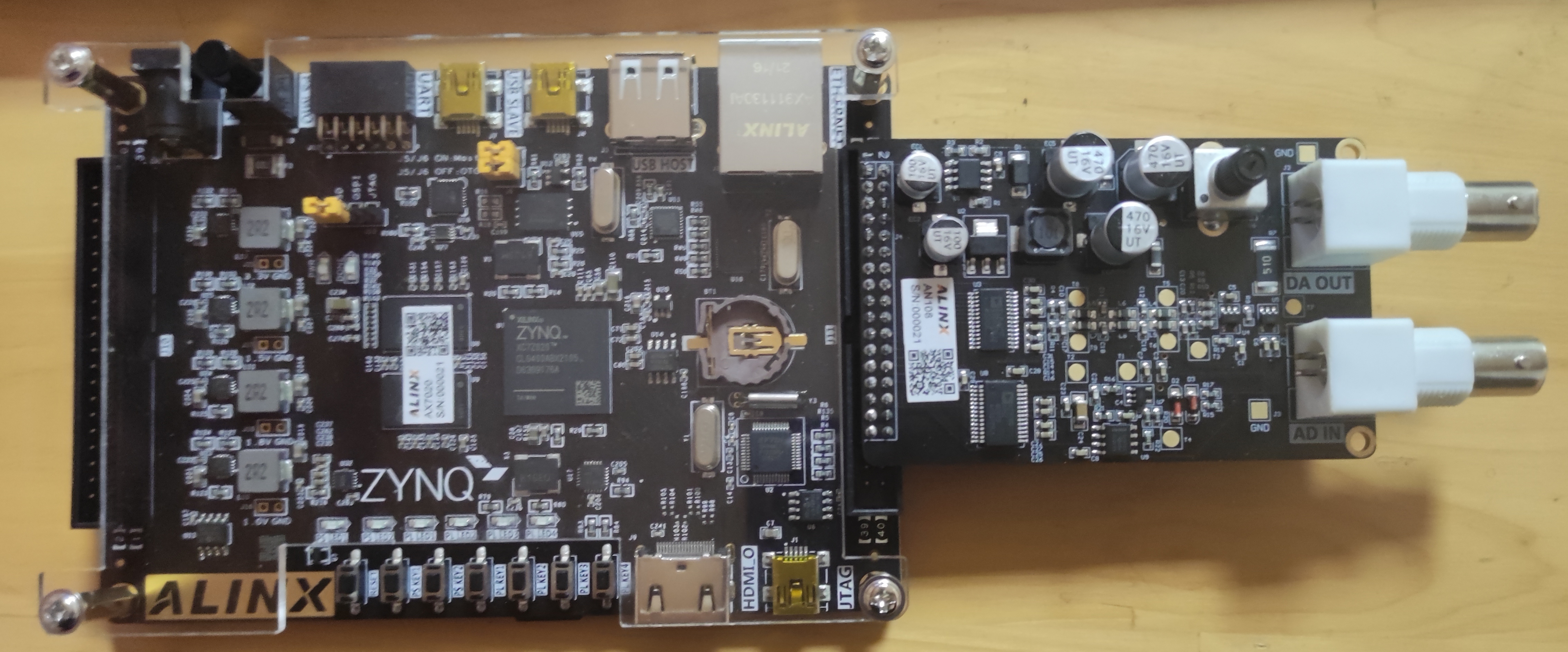
1. Note that AN108 is a 34 pin plug. Pay attention to its insertion position. Align pin 1 with zynq base plate and do not insert it wrong.
2. The passband of the low-pass filter of Heijin AN108 is about 0-20MHz.
3. Based on the experimental scheme of "DDS IP digital waveform synthesis DAC", 50MHz clock frequency is used and DAC is used to output sine wave.
4. The DAC output analog signal is self looped to the input of ADC.
5. MMCM frequency division is used to provide 25MHz sampling clock for ADC.
6. Use ILA to capture the output data of ADC, with no less than 2048 samples.
7. Use Matlab to analyze ADC data spectrum.
8. Change the frequency word with VIO to generate 1MHz and 3MHz sinusoidal signals. Analyze the ILA data with Matlab to verify that the spectrum is correct.
This experiment is based on "DDS IP digital waveform synthesis DAC", which is in engineering DDS_ The changes based on test, the changes involved or the added files will be mentioned in the article. For the specific process of DDS IP digital waveform synthesis experiment, please refer to the blog: ZYNQ FPGA experiment -- DDS IP digital waveform synthesis.
The experiment was also conducted in High speed AD/DA verification experiment of ZYNQ The experiment is a synthesis of the above two experiments.
1, Introduction to ADDA module
The model of ADDA module used in this experiment is AN108, which is shown in the figure below.
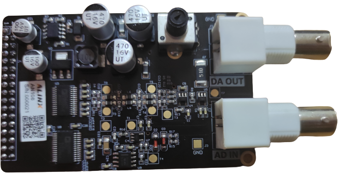
Among them, the maximum sampling rate of ADC is 32MHz and the accuracy is 8 bits, and the maximum sampling rate of DAC is 125MHz and the accuracy is 8 bits.
The ADDA module passes through both AD IN port and DA OUT port BNC interface Connected to the outside world.
The hardware structure diagram of AN108 is shown in the figure below.
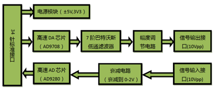
The Da circuit consists of high-speed Da chip AD9708, 7th order Butterworth low-pass filter, amplitude adjustment circuit and signal output interface. High speed Da chip AD9708 is an 8-bit, 125MSPS DA conversion chip with built-in 1.2V reference voltage and differential current output. After the differential output of AD9708 chip, in order to prevent noise interference, a 7th order Butterworth low-pass filter with a bandwidth of 40MHz is connected to the circuit. After the filter, two high-performance 145MHz bandwidth operational amplifiers AD8056 are connected to realize the functions of differential single terminal and amplitude adjustment, so as to maximize the performance of the whole circuit. The amplitude adjustment uses a 5K potentiometer, so the final output range is - 5V-5v, i.e. 10Vpp.
It should be noted that the accuracy of the circuit breaker is not very accurate, and there is a certain error in the final output. It is possible that the waveform amplitude cannot reach 10Vpp, or there may be problems such as waveform clipping, which are normal.
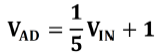
The ad circuit consists of high-speed AD chip AD9280, attenuation circuit and signal input interface. High speed DA chip AD9280 is an 8-bit, 32MSPS AD conversion chip. Before the signal enters the chip AD9280, an AD8056 chip is used to build the attenuation circuit. The input range of the interface is - 5V to 5V. After passing through the attenuation circuit, the input range meets the input range of the ad chip, i.e. 0~2V. The corresponding conversion formula is as follows.
The connection between the black gold 7020 development board and the ADDA module is shown in the figure below. The 1-pin and 2-pin and 39-pin and 40 pin of the row pin of the development board are marked on the development board, and the 1-pin and 2-pin of the ADDA module are also marked on the ADDA module. Since the AN108 is 34 pin and the row pin of the development board is 40 pin, it should be noted not to insert it upside down. First align the 1-pin and 2-pin of the ADDA module with the 1-pin and 2-pin port of the development board, Then insert it from top to bottom.
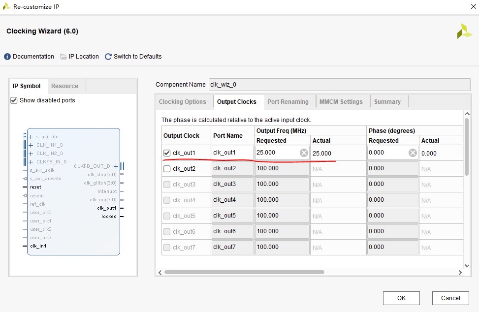
2, Add PLL IP core
A 25MHz clock is generated with PLL to provide sampling clock for ADC.
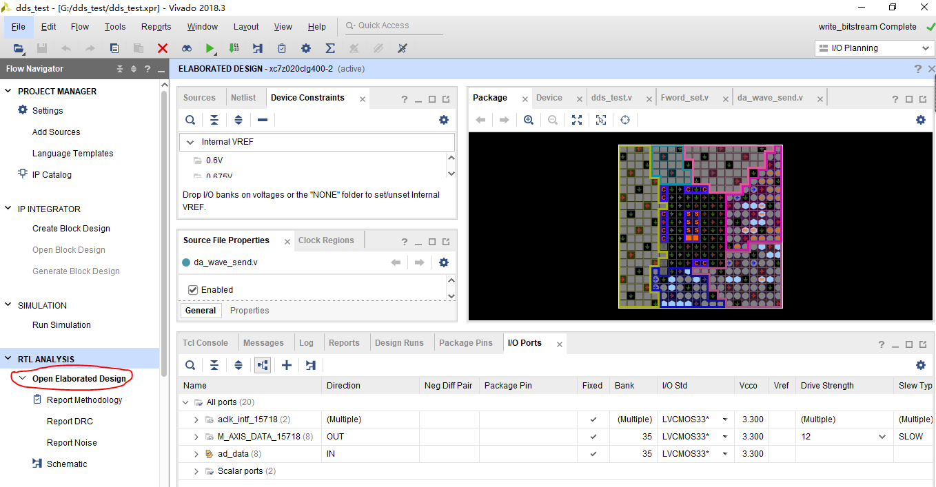
First, operate according to the sequence number in the figure below. Find the Clocking Wizard and double-click to open it.

Add a clock output under Output Clocks with the frequency set to 25MHz. Other options remain the default. Click OK, and then click Generate.
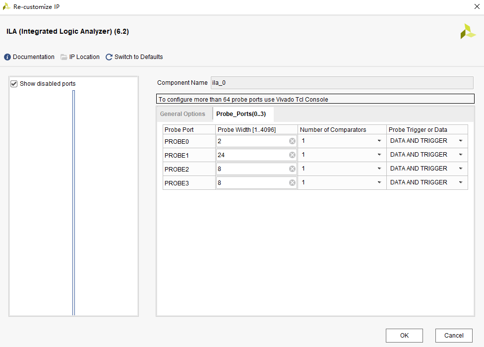
3, Add ILA IP core
The setting of each column under ILA is shown in the figure below.
Four probes are set here to monitor frequency word control bit (2 bits), frequency word (24 bits), ad data (8 bits) and da data (8 bits).
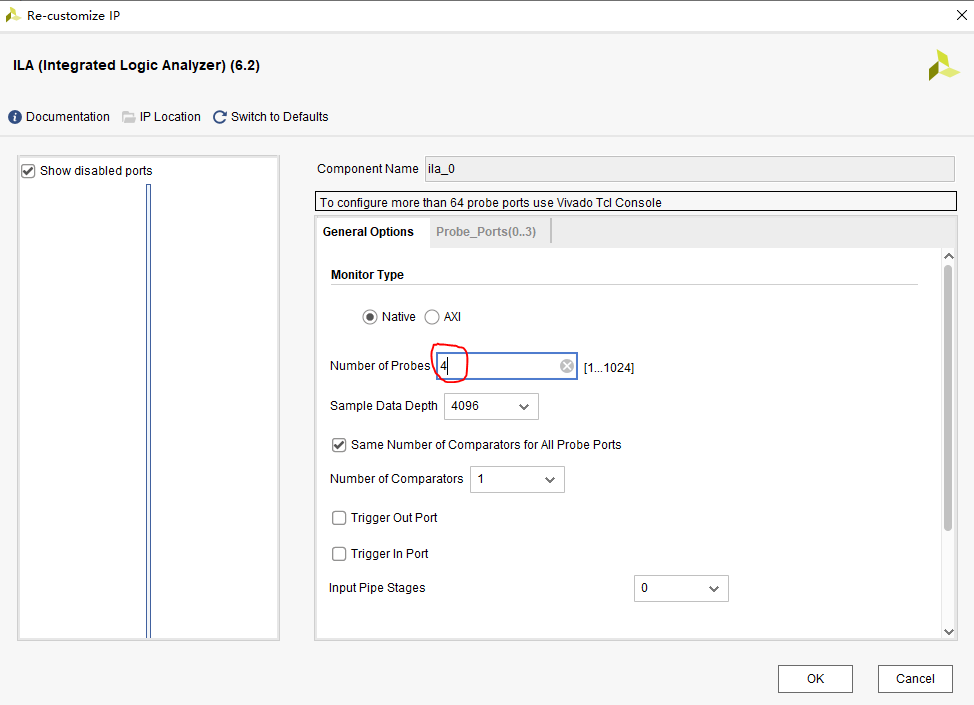
The setting of the number of probes is shown in the figure below.
After the above settings are successful, click OK, and then click Generate.
4, DDS IP core and VIO IP core
VIO IP core and experiment ZYNQ FPGA experiment -- DDS IP digital waveform synthesis Same, no change here.
The difference between DDS IP core and the above experiment is that in Parameter Selection, Hardware Parameters is selected instead of System Parameters, and 8-bit output width is selected for Hardware Parameters, because ADDA module can only transmit data with 8-bit width at most.
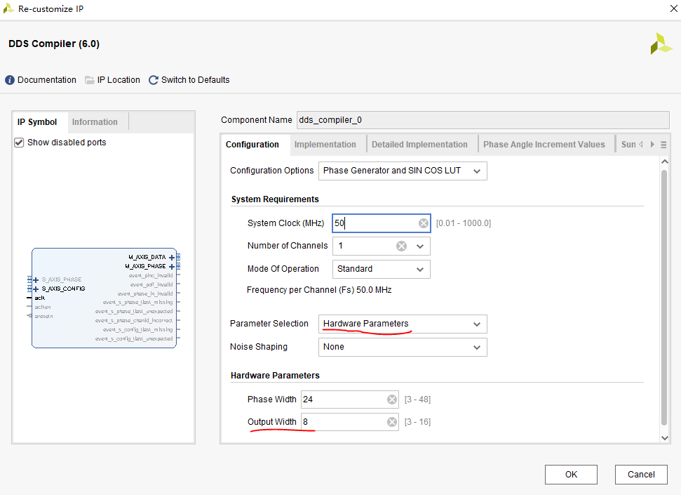
Other options can be set by default.
5, Write test program
The file directory structure of this experiment is shown in the figure below.
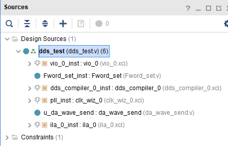
File DDS_ test. The code written in V is as follows.
//The code refers to the usage of vivado VIO IP and the official documents of punctual atom. See the summary
`timescale 1ns / 1ps

module dds_test(
    input           sys_clk,        //System clock 50MHz t = 20ns
    input           rst_n,           //System reset

     //DA chip interface
    output                da_clk,  //DA(AD9708) drives the clock and supports 125Mhz clock at most
    output    [7:0]       da_data,  //Data output to DA
    //AD chip interface
    input     [7:0]       ad_data,  //AD input data
    //Analog input voltage out of range mark (not used in this test)
    //input                 ad_ OTR, / / 0: in range 1: out of range
    output                ad_clk         //AD(AD9280) drives the clock and supports 32Mhz clock at most
    );

//----------VIO key control frequency control word (key_PINC)--------------//
 wire [1:0] key_PINC;
 vio_0 vio_0_inst (
      .clk(sys_clk),                // input wire clk
      .probe_out0(key_PINC)  // output wire [1 : 0] probe_out0
);

//---------------Signal frequency control module--------------//
wire  [23:0]   Fword ;  //Frequency word
Fword_set Fword_set_inst(
        //input
        .clk        (sys_clk),
        .rst_n      (rst_n),
        .key_PINC   (key_PINC),
        //output
        .Fword      (Fword)
        );

//---------------DDS module--------------//
//input
wire [0:0]   fre_ctrl_word_en  ;
//output
wire [0:0]   m_axis_data_tvalid    ;
wire [7:0]   m_axis_data_tdata     ;
wire [0:0]   m_axis_phase_tvalid   ;
wire [23:0]  m_axis_phase_tdata    ;

assign fre_ctrl_word_en=1'b1;

//Instantiated DDS IP
dds_compiler_0 dds_compiler_0_inst (
  .aclk                 (sys_clk                ),    // input wire aclk
  .s_axis_config_tvalid (fre_ctrl_word_en       ),    // input wire s_axis_config_tvalid
  .s_axis_config_tdata  (Fword                  ),    // input wire [23: 0] s_axis_config_tdata

  .m_axis_data_tvalid   (m_axis_data_tvalid     ),    // output wire m_axis_data_tvalid
  .m_axis_data_tdata    (m_axis_data_tdata      ),    // output wire [7 : 0] m_axis_data_tdata
  .m_axis_phase_tvalid  (m_axis_phase_tvalid    ),    // output wire m_axis_phase_tvalid
  .m_axis_phase_tdata   (m_axis_phase_tdata     )     // output wire [23 : 0] m_axis_phase_tdata
);

//Instantiated PLL
clk_wiz_0 pll_inst
   (
    // Clock out ports
    .clk_out1(ad_clk),     // Give ad_clk 25MHz frequency
    // Status and control signals
    .reset(~rst_n), // input reset
    .locked(locked),       // output locked
   // Clock in ports
    .clk_in1(sys_clk)     // input clk_in1
 );

//DA data transmission
da_wave_send u_da_wave_send(
    .clk         (sys_clk),
    .rst_n       (rst_n),
    .rd_data     (m_axis_data_tdata),
    .da_clk      (da_clk),
    .da_data     (da_data)
    );

//ILA collects AD data
ila_0 ila_0_inst (
	.clk(sys_clk), // input wire clk

	.probe0(key_PINC), // input wire [1:0]  probe0
	.probe1(Fword), // input wire [23:0]  probe1
	.probe2(da_data), // input wire [7:0]  probe2
	.probe3(ad_data) // input wire [7:0]  probe3
);

endmodule
File fword_ set. The code written in V is as follows.
//The code comes from the blog: vivado vio. See the summary for the usage of IP
`timescale 1ns / 1ps

module Fword_set(
    input               clk         ,
    input               rst_n       ,
    input  [1:0]        key_PINC    ,

    output reg [23:0]   Fword
    );

always@(*)
begin
    case(key_PINC)
        0:  Fword <= 'h51eb;     //1Mhz 20971.52 rounded off
        1:  Fword <= 'ha3d7;     //2Mhz 41943.04 rounding
        2:  Fword <= 'hf5c2;     //3Mhz 62914.56 rounded off
        //3:  Fword <= 'h33333;    // 10MHz 209715.2 rounding
    endcase
end

endmodule
File Da_ wave_ send. Write the following code in V.
//This code comes from punctual atom
module da_wave_send(
    input                 clk    ,  //Clock
    input                 rst_n  ,  //Reset signal, active at low level
    input        [7:0]    rd_data,  //Read out data
    //DA chip interface
    output                da_clk ,  //DA(AD9708) drives the clock and supports 125Mhz clock at most
    output       [7:0]    da_data   //Data output to DA
);

//parameter frequency regulation control
parameter  FREQ_ADJ = 8'd5;  //Frequency regulation, freq_ The greater the value of adj, the lower the final output frequency, ranging from 0 to 255

//reg define
reg    [7:0]    freq_cnt  ;  //Frequency regulation counter

//Data Rd_ The data is updated at the rising edge of clk, so the DA chip latches the data at the falling edge of clk when it is stable
//And DA is actually da_ The rising edge of clk latches data, so the clock is reversed, so the falling edge of clk is equivalent to da_ Rising edge of clk
assign  da_clk = ~clk;
assign  da_data = rd_data;   //Assign the read data to the DA data port

//Frequency regulation counter
always @(posedge clk or negedge rst_n) begin
    if(rst_n == 1'b0)
        freq_cnt <= 8'd0;
    else if(freq_cnt == FREQ_ADJ)
        freq_cnt <= 8'd0;
    else
        freq_cnt <= freq_cnt + 8'd1;
end

endmodule
6, Pin assignment
The schematic diagram of 34 pin arrangement of ADDA module AN108 is as follows.

The schematic diagram of J11 expansion port of black gold development board is as follows.
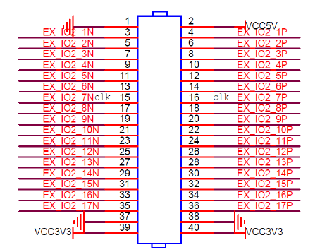
Among them, the pin number corresponding to J11 expansion port is shown in the table below.
| J11 pin | Signal name | ZYNQ pin name | ZYNQ pin number |
|---|---|---|---|
| PIN1 | GND | - | - |
| PIN2 | +5V | - | - |
| PIN3 | EX_IO2_1N | IO_L6N_T0_35 | F17 |
| PIN4 | EX_IO2_1P | IO_L6P_T0_35 | F16 |
| PIN5 | EX_IO2_2N | IO_L15N_T2_35 | F20 |
| PIN6 | EX_IO2_2P | IO_L15P_T2_35 | F19 |
| PIN7 | EX_IO2_3N | IO_L18N_T2_35 | G20 |
| PIN8 | EX_IO2_3P | IO_L18P_T2_35 | G19 |
| PIN9 | EX_IO2_4N | IO_L14N_T2_35 | H18 |
| PIN10 | EX_IO2_4P | IO_L14P_T2_35 | J18 |
| PIN11 | EX_IO2_5N | IO_L9N_T1_35 | L20 |
| PIN12 | EX_IO2_5P | IO_L9P_T1_35 | L19 |
| PIN13 | EX_IO2_6N | IO_L7N_T1_35 | M20 |
| PIN14 | EX_IO2_6P | IO_L7P_T1_35 | M19 |
| PIN15 | EX_IO2_7N | IO_L12N_T1_35 | K18 |
| PIN16 | EX_IO2_7P | IO_L12P_T1_35 | K17 |
| PIN17 | EX_IO2_8N | IO_L10N_T1_35 | J19 |
| PIN18 | EX_IO2_8P | IO_L10P_T1_35 | K19 |
| PIN19 | EX_IO2_9N | IO_L17N_T2_35 | H20 |
| PIN20 | EX_IO2_9P | IO_L17P_T2_35 | J20 |
| PIN21 | EX_IO2_10N | IO_L11N_T1_35 | L17 |
| PIN22 | EX_IO2_10P | IO_L11P_T1_35 | L16 |
| PIN23 | EX_IO2_11N | IO_L8N_T1_35 | M18 |
| PIN24 | EX_IO2_11P | IO_L8P_T1_35 | M17 |
| PIN25 | EX_IO2_12N | IO_L4N_T0_35 | D20 |
| PIN26 | EX_IO2_12P | IO_L4P_T0_35 | D19 |
| PIN27 | EX_IO2_13N | IO_L5N_T0_35 | E19 |
| PIN28 | EX_IO2_13P | IO_L5P_T0_35 | E18 |
| PIN29 | EX_IO2_14N | IO_L16N_T2_35 | G18 |
| PIN30 | EX_IO2_14P | IO_L16P_T2_35 | G17 |
| PIN31 | EX_IO2_15N | IO_L13N_T2_35 | H17 |
| PIN32 | EX_IO2_15P | IO_L13P_T2_35 | H16 |
| PIN33 | EX_IO2_16N | IO_L19N_T3_35 | G15 |
| PIN34 | EX_IO2_16P | IO_L19P_T3_35 | H15 |
| PIN35 | EX_IO2_17N | IO_L20N_T3_35 | J14 |
| PIN36 | EX_IO2_17P | IO_L20P_T3_35 | K14 |
| PIN37 | GND | - | - |
| PIN38 | GND | - | - |
| PIN39 | +3.3V | - | - |
| PIN40 | +3.3V | - | - |
According to the pin numbers corresponding to each pin in the above table, combined with the schematic diagram of AN108 and the schematic diagram of J11 expansion port, open the pin configuration interface and assign pins in turn.
7, Connect development board test
Connect the development board, click Generate Bitstream to Generate Bitstream file and download it to the development board.
At this time, HW will appear_ ila_ 1 and hw_vios two windows, where HW_ It is used to adjust the corresponding frequency window of 1MHz, vi00, where the corresponding frequency is 2MHz_ ila_ 1 window is used to view the output waveform.
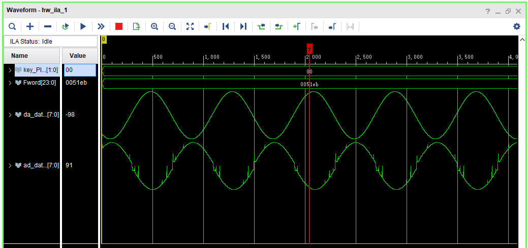
The output waveform observed at 1MHz output frequency under ILA is shown in the figure below.
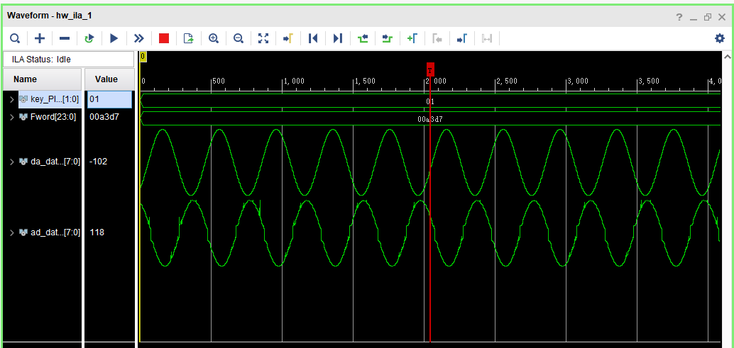
The output waveform observed at 2MHz output frequency under ILA is shown in the figure below.
The output waveform observed at 3MHz output frequency under ILA is shown in the figure below.
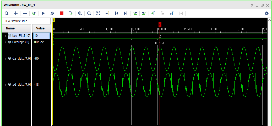
As can be seen from the above output waveform diagram, the sine wave of Da output is relatively regular without burr, while the sine wave of AD input has burr, and there is a difference of half a sine wave cycle between DA output and AD input.
8, Analysis of output waveform in Matlab
The sine waves corresponding to different output frequencies under the above ILA are exported as CSV files, and then analyzed in Matlab.
Create a new script file and write the following code.
csv_row6 = iladata{:,6};  %take out csv The sixth column of data in the file
csv_row7 = iladata{:,7};  %take out csv The seventh column of data in the file
fs=50000000;    %Set the sampling frequency to 50 MHz
N=4096;         %Sampling point
n=0:N-1;
t=n/fs;
f=n*fs/N;       %Frequency sequence
figure;
subplot(2,1,1);plot(t,csv_row6);grid on;title('1MHz-DA Time domain waveform');
y1=abs(fft(csv_row6,N));
subplot(2,1,2);plot(f,y1,'r');grid on;title('1MHz-DA spectrum');
figure;
subplot(2,1,1);plot(t,csv_row7);grid on;title('1MHz-AD Time domain waveform');
y2=abs(fft(csv_row7,N));
subplot(2,1,2);plot(f,y2,'r');grid on;title('1MHz-AD spectrum');
The output diagram of DA with output frequency of 1MHz is as follows.

The output diagram of AD with output frequency of 1MHz is as follows.

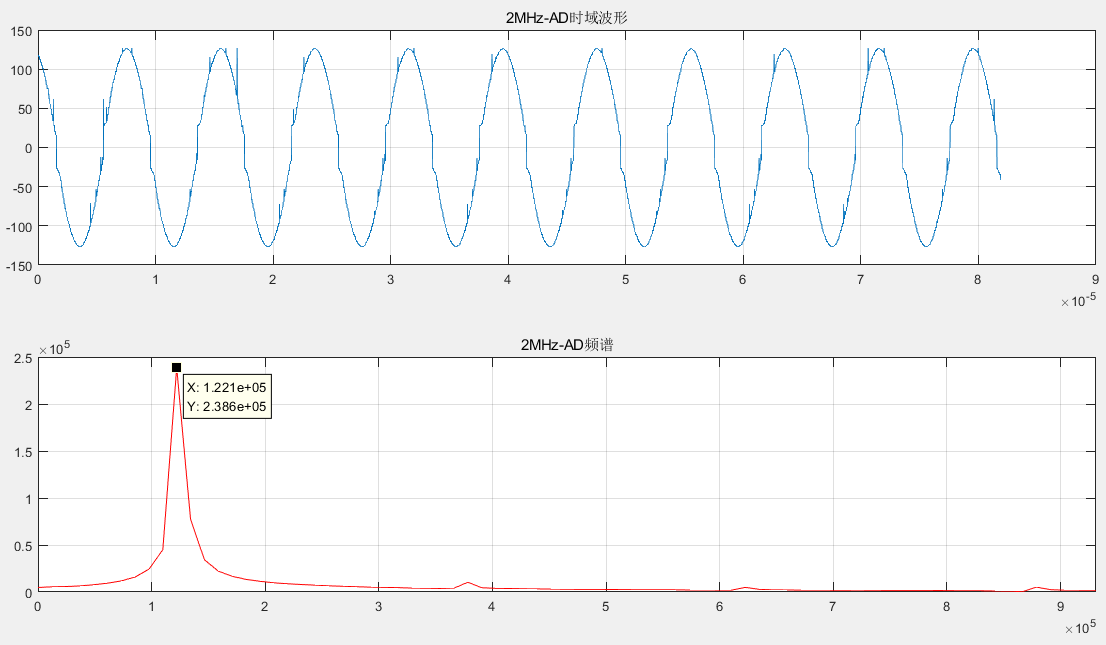
In the same way, the output diagrams with output frequencies of 2MHz and 3MHz are obtained.
The output diagram of DA with output frequency of 2MHz is as follows.

The output diagram of AD with output frequency of 2MHz is as follows.
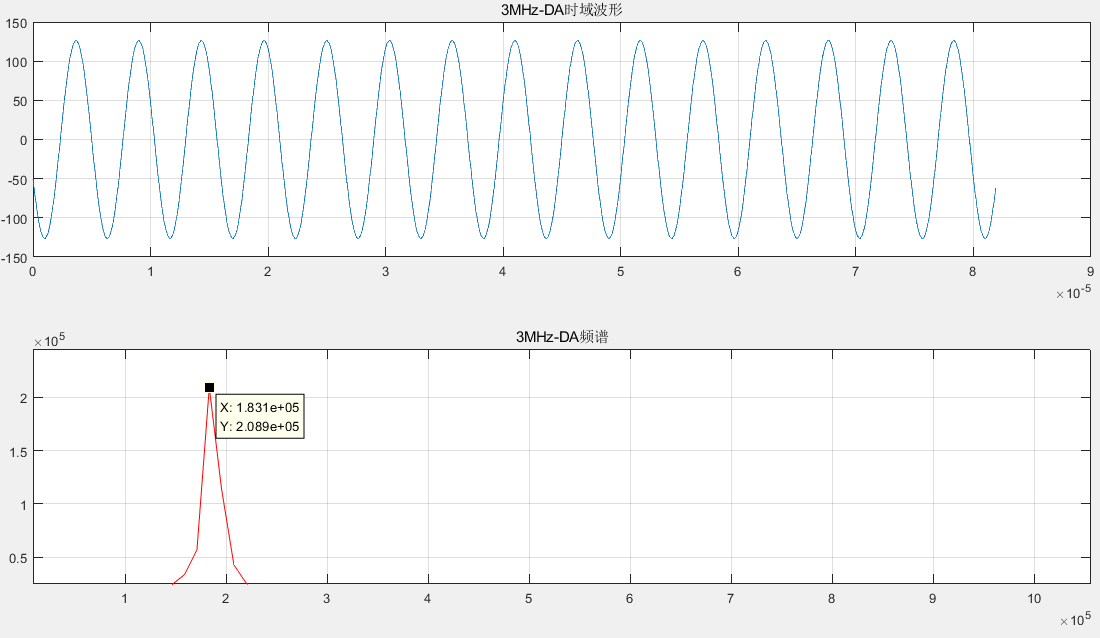
The output diagram of DA with output frequency of 3MHz is as follows.
The output diagram of AD with output frequency of 3MHz is as follows.
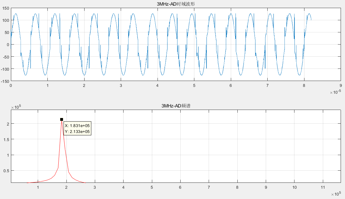
Although the above output results of this experiment are not like the DDS IP digital waveform synthesis experiment, the corresponding output frequency can be read out through the spectrum, and there is a certain difference between the output frequency and the real frequency, which may be due to the small number of data bits, it can be seen from the analysis of the spectrum of different output frequencies by Matlab that 1MHz The DA output frequency and AD input frequency corresponding to 2MHz and 3MHz output frequencies are equal, and the multiple relationship between the real frequency corresponding to each output frequency is still valid.
summary
The above is all the contents of ZYNQ FPGA experiment - AD/DA test. This experiment is ZYNQ FPGA experiment -- DDS IP digital waveform synthesis and High speed AD/DA verification experiment of ZYNQ For the synthesis of these two experiments, it should be noted that there is a difference when adding DDS IP core. The number of ILA probes is determined according to the number of signals they need to observe. In particular, pay attention to the changes of some details, otherwise errors will occur during compilation.
References:
Punctual atom – course_s1_ZYNQ those things - FPGA experiment v1 06.pdf
ALINX black gold AX7020 development board user manual v2 2.pdf
Pilot ZYNQ's FPGA Development Guide_ V2. 0 pdf
This article refers to the blog:
Usage of vivado VIO IP
FPGA digital signal processing foundation -- Xilinx DDS IP application