Write in front
In AXIS, we packaged the IP of two axi4 stream interfaces (one master and one slave)( Take you to a quick start AXI4 bus -- AXI4 stream (2) -- Xilinx AXI4 stream interface IP source code simulation analysis ), the two IPS are simulated and analyzed, and the code provided by XILINX is also studied. In this article, we also package the IP of two axi4 Lite interfaces (one master and one slave) to learn its simulation and original code. Limited to space, I will write two articles. This article will write the axi4 Lite slave interface.
1. Call IP
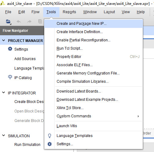
First create a new project, and then click Tools-----create and package new ip
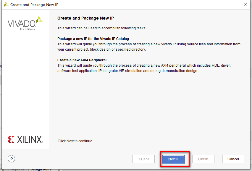
Click Next
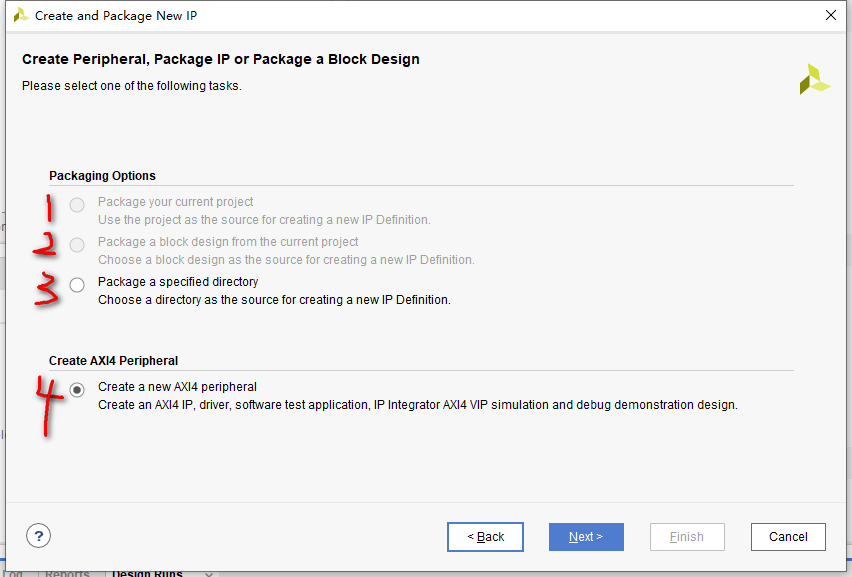
Select option 4 and click Next. The meaning of each option:
- 1 --- package the current project as an IP core
- 2 ---- package the module design of the current project into IP core
- 3 ---- package a specific folder directory as an IP core
- 4 ---- create an IP core with AXI interface
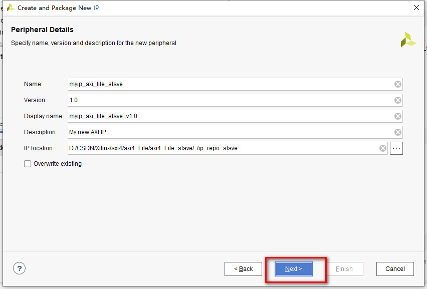
Fill in the IP information (basically no modification, only change the name for subsequent management), and click Next
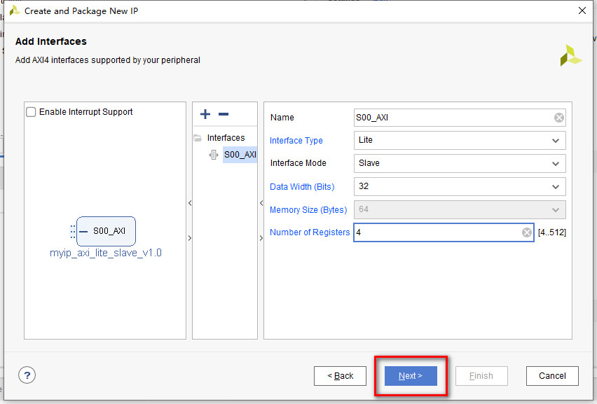
Select Lite interface, slave Slave interface for interface type, 32-bit data width, and 4 registers (this register is mainly used on SOC or ZYNQ, so you don't need to know too much here). Click Next
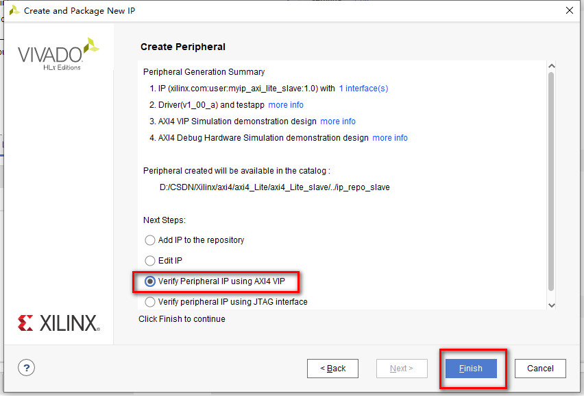
Here comes the wonderful one. Select the third one, use AXI4 VIP to verify the IP, and then click Next. (AXI4 VIP is an IP core of XILINX, which can provide a variety of connection modes to verify the AXI interface. It is very intimate and convenient to use. We will write related articles later. Please look forward to it.)
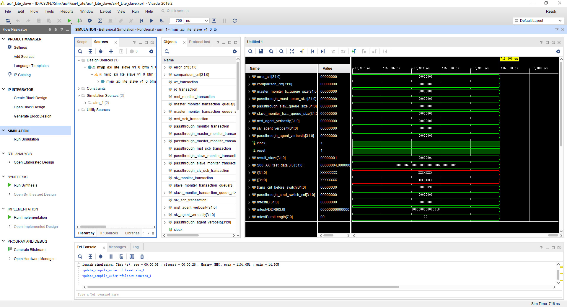
At this time, the following interface is automatically generated, and even opens the simulation interface for you.
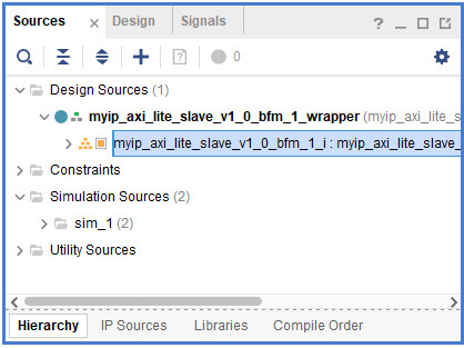
Let's not rush to simulate first. Let's look at the structure of the whole project first. Double click the BD file in the figure below,
The pop-up structure block diagram is as follows:,
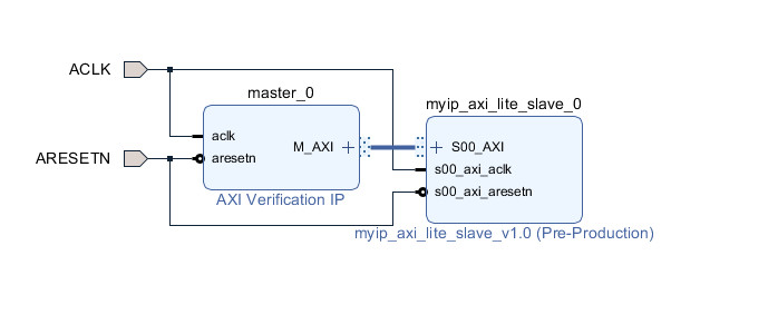
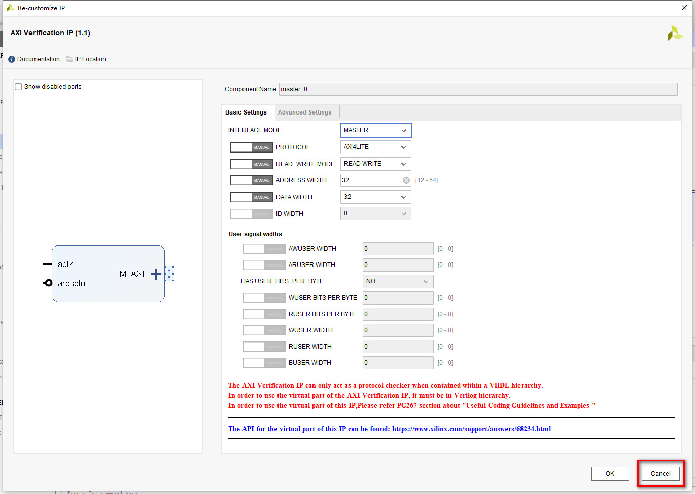
The whole project consists of two parts: 1. Our packaged IP, whose interface is aix4 Lite slave; 2. AXI Verification IP, an AXI Verification IP, provides a variety of verification methods and powerful functions. Double click the IP to see its built-in customization information:
It can be seen that it can select the interface mode to realize the host or slave or through function; Optional protocol type, address bit width, data bit width, etc. We don't move it here, just cancel
Then click to operate as shown in the figure below, right-click the BD file and select generate output products to generate the source code:
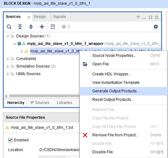
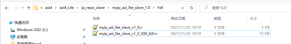
In this path, the source code (the second file) file and the top-level instantiation file (the first file, which is not controlled) are generated
2. Source code analysis of Slave interface
Open the source code generated by the above section (Note: I deleted the source's notes, otherwise it was too long. I optimized the format again, mainly aligning. By the way, I could make complaints about CSDN code):
`timescale 1 ns / 1 ps
//NO.1 ---------------------------------------- input / output port-------------------------------------------
	module myip_axi_lite_slave_v1_0_S00_AXI #
	(
		parameter integer C_S_AXI_DATA_WIDTH	= 32,
		parameter integer C_S_AXI_ADDR_WIDTH	= 4
	)
	(
//Global signal
		input 	wire  								S_AXI_ACLK,
		input 	wire  								S_AXI_ARESETN,
//Write address channel
		input 	wire [C_S_AXI_ADDR_WIDTH-1 : 0] 	S_AXI_AWADDR,
		input 	wire  								S_AXI_AWVALID,
		output 	wire  								S_AXI_AWREADY,
//Write data channel
		input 	wire [C_S_AXI_DATA_WIDTH-1 : 0] 	S_AXI_WDATA,
		input 	wire [(C_S_AXI_DATA_WIDTH/8)-1 : 0] S_AXI_WSTRB,
		input 	wire  								S_AXI_WVALID,
		output 	wire  								S_AXI_WREADY,
//Write response channel
		output 	wire [1 : 0] 						S_AXI_BRESP,
		output 	wire  								S_AXI_BVALID,
		input 	wire  								S_AXI_BREADY,
//Read address channel
		input 	wire [C_S_AXI_ADDR_WIDTH-1 : 0] 	S_AXI_ARADDR,
		input 	wire [2 : 0] 						S_AXI_ARPROT,
		input 	wire  								S_AXI_ARVALID,
		output 	wire  								S_AXI_ARREADY,
//Read data channel
		output wire [C_S_AXI_DATA_WIDTH-1 : 0] 		S_AXI_RDATA,
		output wire [1 : 0] 						S_AXI_RRESP,
		output wire  								S_AXI_RVALID,
		input  wire  								S_AXI_RREADY
	);

//NO.2 ---------------------------------------- register definition------------------------------------------------------------
	//Axi4 Lite interface related
	reg [C_S_AXI_ADDR_WIDTH-1 : 0] 					axi_awaddr;
	reg  											axi_awready;
	reg  											axi_wready;
	reg [1 : 0] 									axi_bresp;
	reg  											axi_bvalid;
	reg [C_S_AXI_ADDR_WIDTH-1 : 0] 					axi_araddr;
	reg  											axi_arready;
	reg [C_S_AXI_DATA_WIDTH-1 : 0] 					axi_rdata;
	reg [1 : 0] 									axi_rresp;
	reg  											axi_rvalid;

	//slave register correlation
	localparam integer ADDR_LSB = (C_S_AXI_DATA_WIDTH/32) + 1;
	localparam integer OPT_MEM_ADDR_BITS = 1;

	reg [C_S_AXI_DATA_WIDTH-1:0]	slv_reg0;
	reg [C_S_AXI_DATA_WIDTH-1:0]	slv_reg1;
	reg [C_S_AXI_DATA_WIDTH-1:0]	slv_reg2;
	reg [C_S_AXI_DATA_WIDTH-1:0]	slv_reg3;
	wire	 						slv_reg_rden;
	wire	 						slv_reg_wren;
	reg [C_S_AXI_DATA_WIDTH-1:0]	reg_data_out;
	integer	 						byte_index;
	reg	 							aw_en;

//NO.3 ---------------------------------------- port assignment definition------------------------------------------------------------
	//Avoid direct operation of the output port by assignment
	assign S_AXI_AWREADY = axi_awready;
	assign S_AXI_WREADY	 = axi_wready;
	assign S_AXI_BRESP	 = axi_bresp;
	assign S_AXI_BVALID	 = axi_bvalid;
	assign S_AXI_ARREADY = axi_arready;
	assign S_AXI_RDATA	 = axi_rdata;
	assign S_AXI_RRESP	 = axi_rresp;
	assign S_AXI_RVALID	 = axi_rvalid;

//NO.4 ---------------------------------------- generate write address preparation signal axi_awready-------------------------------------------
	always @( posedge S_AXI_ACLK )
	begin
	  if ( S_AXI_ARESETN == 1'b0 )
	    begin
	      axi_awready <= 1'b0;						//The slave is not ready to receive a write address
	      aw_en <= 1'b1;							//Write transactions can be performed
	    end
	  else
	    begin
	      if (~axi_awready && S_AXI_AWVALID && S_AXI_WVALID && aw_en)	//The host is ready to write addresses and data, the system can execute write transactions, and the slave is not ready
	        begin
	          axi_awready <= 1'b1;					//The slave is ready to receive the write address
	          aw_en <= 1'b0;						//Executing write transaction
	        end
	        else if (S_AXI_BREADY && axi_bvalid)	//Once the write transaction is responded, it represents the end of a write operation
	            begin
	              aw_en <= 1'b1;					//When the response signal ends, the write transaction can be executed
	              axi_awready <= 1'b0;				//The slave is not ready to receive a write address
	            end
	      else
	        begin
	          axi_awready <= 1'b0;					//Generally, the slave is not ready
	        end
	    end
	end

//NO.5 ---------------------------------------- latch write address signal axi_awaddr-------------------------------------------
	always @( posedge S_AXI_ACLK )
	begin
	  if ( S_AXI_ARESETN == 1'b0 )
	    begin
	      axi_awaddr <= 0;
	    end
	  else
	    begin
		  //The host is ready to write addresses and data, the system can execute write transactions, and the slave is not ready
	      if (~axi_awready && S_AXI_AWVALID && S_AXI_WVALID && aw_en)
	        begin
	          axi_awaddr <= S_AXI_AWADDR;			//In the next cycle, the slave is ready to receive data and register the address for later analysis
	        end
	    end
	end

//NO.6 ---------------------------------------- generate write data preparation signal axi_wready-------------------------------------------
	always @( posedge S_AXI_ACLK )
	begin
	  if ( S_AXI_ARESETN == 1'b0 )
	    begin
	      axi_wready <= 1'b0;
	    end
	  else
	    begin
		  //Write data is not ready, write data is valid, write address is valid, and write transactions can be executed
	      if (~axi_wready && S_AXI_WVALID && S_AXI_AWVALID && aw_en )
	        begin
	          axi_wready <= 1'b1;					//Slave ready to write data
	        end
	      else
	        begin
	          axi_wready <= 1'b0;					//Generally, the slave is not ready
	        end
	    end
	end

//NO.7 ---------------------------------------- write the data on the AXI bus to the register in the slave-------------------------------------------
	assign slv_reg_wren = axi_wready && S_AXI_WVALID && axi_awready && S_AXI_AWVALID;	//When preparing to write data, pull up the register write enable to align with the AXI bus write data

	always @( posedge S_AXI_ACLK )
	begin
	  if ( S_AXI_ARESETN == 1'b0 )
	    begin
	      slv_reg0 <= 0;
	      slv_reg1 <= 0;
	      slv_reg2 <= 0;
	      slv_reg3 <= 0;
	    end
	  else begin
	    if (slv_reg_wren)														//Register write enable valid
	      begin
	        case ( axi_awaddr[ADDR_LSB+OPT_MEM_ADDR_BITS:ADDR_LSB] )			//Determine which register should be written according to the write address
	          2'h0:
	            for ( byte_index = 0; byte_index <= (C_S_AXI_DATA_WIDTH/8)-1; byte_index = byte_index+1 )
	              if ( S_AXI_WSTRB[byte_index] == 1 ) begin						//Judge whether the current BYTE is valid (i.e. whether the mask function is effective)
	                slv_reg0[(byte_index*8) +: 8] <= S_AXI_WDATA[(byte_index*8) +: 8];
	              end
	          2'h1:
	            for ( byte_index = 0; byte_index <= (C_S_AXI_DATA_WIDTH/8)-1; byte_index = byte_index+1 )
	              if ( S_AXI_WSTRB[byte_index] == 1 ) begin
	                slv_reg1[(byte_index*8) +: 8] <= S_AXI_WDATA[(byte_index*8) +: 8];
	              end
	          2'h2:
	            for ( byte_index = 0; byte_index <= (C_S_AXI_DATA_WIDTH/8)-1; byte_index = byte_index+1 )
	              if ( S_AXI_WSTRB[byte_index] == 1 ) begin
	                slv_reg2[(byte_index*8) +: 8] <= S_AXI_WDATA[(byte_index*8) +: 8];
	              end
	          2'h3:
	            for ( byte_index = 0; byte_index <= (C_S_AXI_DATA_WIDTH/8)-1; byte_index = byte_index+1 )
	              if ( S_AXI_WSTRB[byte_index] == 1 ) begin
	                slv_reg3[(byte_index*8) +: 8] <= S_AXI_WDATA[(byte_index*8) +: 8];
	              end
	          default : begin
	                      slv_reg0 <= slv_reg0;
	                      slv_reg1 <= slv_reg1;
	                      slv_reg2 <= slv_reg2;
	                      slv_reg3 <= slv_reg3;
	                    end
	        endcase
	      end
	  end
	end

//NO.8 ---------------------------------------- generate write response signal axi_bvalid, response value axi_bresp-------------------------------------------
	always @( posedge S_AXI_ACLK )
	begin
	  if ( S_AXI_ARESETN == 1'b0 )
	    begin
	      axi_bvalid  <= 0;
	      axi_bresp   <= 2'b0;
	    end
	  else
	    begin
		  //Data is being written, and the slave is not ready to respond to a valid signal
	      if (axi_awready && S_AXI_AWVALID && ~axi_bvalid && axi_wready && S_AXI_WVALID)
	        begin
	          axi_bvalid <= 1'b1;				//The slave pulls up the response valid signal and waits for the host to reply and prepare to receive the response signal S_AXI_BREADY
	          axi_bresp  <= 2'b0; 				//Access succeeded: 'OKAY' response
	        end                   				//Other response judgments are not supported
	      else
	        begin
	          if (S_AXI_BREADY && axi_bvalid) 	//Handshake successful
	            begin
	              axi_bvalid <= 1'b0; 			//Pull down axi_bvalid (only need to maintain one clock cycle)
	            end
	        end
	    end
	end

//NO.9 ---------------------------------------- register read address S_AXI_ARADDR, generate read data preparation signal-------------------------------------------
	always @( posedge S_AXI_ACLK )
	begin
	  if ( S_AXI_ARESETN == 1'b0 )
	    begin
	      axi_arready <= 1'b0;
	      axi_araddr  <= 32'b0;
	    end
	  else
	    begin
	      if (~axi_arready && S_AXI_ARVALID)	//The host is ready to send the read address, but the slave is not ready to receive it
	        begin
	          axi_arready <= 1'b1;				//Slave ready to read address
	          axi_araddr  <= S_AXI_ARADDR;		//Register the address to be read
	        end
	      else
	        begin
	          axi_arready <= 1'b0;				//In other cases, the slave is not ready to receive the read address by default
	        end
	    end
	end

//NO.10 ---------------------------------------- generate read response signal axi_rvalid, read response value axi_rresp-------------------------------------------
	always @( posedge S_AXI_ACLK )
	begin
	  if ( S_AXI_ARESETN == 1'b0 )
	    begin
	      axi_rvalid <= 0;
	      axi_rresp  <= 0;
	    end
	  else
	    begin
	      if (axi_arready && S_AXI_ARVALID && ~axi_rvalid)				//The handshake of the read address channel is successful, and the data read from the slave is invalid
	        begin
	          axi_rvalid <= 1'b1;										//The data read from the computer is valid
	          axi_rresp  <= 2'b0; 										// 'OKAY' response
	        end
	      else if (axi_rvalid && S_AXI_RREADY)							//Read data channel handshake completed
	        begin
	          axi_rvalid <= 1'b0;										//axi_rvalid (only need to maintain one clock cycle)
	        end
	    end
	end

//NO.11 ---------------------------------------- generate register read enable signal and take out the value of register-------------------------------------------
	assign slv_reg_rden = axi_arready & S_AXI_ARVALID & ~axi_rvalid;	//Register read enable is aligned with read data transactions

	always @(*)
	begin
	      // Address decoding for reading registers
	      case ( axi_araddr[ADDR_LSB+OPT_MEM_ADDR_BITS:ADDR_LSB] )		//The value of which register needs to be read out according to the address
	        2'h0   : reg_data_out <= slv_reg0;							//Assign the value of the register to reg_data_out
	        2'h1   : reg_data_out <= slv_reg1;
	        2'h2   : reg_data_out <= slv_reg2;
	        2'h3   : reg_data_out <= slv_reg3;
	        default : reg_data_out <= 0;
	      endcase
	end

//NO.12 ---------------------------------------- generate read data Axi on the bus_ rdata-------------------------------------------
	always @( posedge S_AXI_ACLK )
	begin
	  if ( S_AXI_ARESETN == 1'b0 )
	    begin
	      axi_rdata  <= 0;
	    end
	  else
	    begin
	      if (slv_reg_rden)					//Read register enable valid
	        begin
	          axi_rdata <= reg_data_out;	//Output the value of the register to the read data channel and put it on the bus for the host to read away
	        end
	    end
	end

	endmodule
The code is long. I will divide it into 12 parts NO.1-12 to explain. Just talk about the general idea. For other contents, please see the code comments.
NO.1:
This part mainly focuses on the instantiation of module ports and parameters.
Parameterization: data bit width 32 bits; Address bit width 4 bits
Module port: the port of axi4 Lite protocol. If you don't remember, you can see here: Take you to a quick start AXI4 bus -- AXI4 Lite chapter (1) -- AXI4 Lite bus
NO.2:
This part mainly defines some registers.
Some of these registers are signals that the slave needs to output to the host. Because they operate in the always block, they need to be defined as reg type.
Others are registers that operate on the slave register of the slave module itself.
NO.3:
This part mainly assigns the value of the defined output register to the output port to avoid directly operating the output port.
NO.4:
This section assigns values to two signals:
Write transaction flag signal aw can be executed_ En (high indicates that a write transaction can be performed once);
Slave preparation signal Axi of write address channel_ Awready (high indicates that the slave can be written to the address)
NO.5:
This part mainly latches the address to be written, which is convenient for later operation on the slave register of the slave.
NO.6:
This part prepares the signal Axi for the slave of the write data channel_ Wready assignment.
NO.7:
This part is mainly based on the address to be written. The main sentence to be written to the slave on the bus is written to the slave register. At the same time, pay attention to s_ AXI_ When the write gate of wstrb is high, it means that the corresponding BYTE on the bus is valid, otherwise it is invalid.
NO.8:
This section assigns values to two signals:
The slave of the write response channel is ready to respond to the signal axi_bvalid, which is pulled high, indicates that the slave is ready to complete a write response.
Write response value replied by slave axi_bresp, whose value is fixed to 0, indicates that the response is successful (other values are not supported temporarily, such as unsuccessful response, etc.)
NO.9:
This section assigns values to two signals:
Slave ready signal Axi of read address channel_ Already, which is pulled high to indicate that the slave is ready to receive the read address
Read address s of the read address channel_ axi_araddr deposit to axi_araddr is used to find the corresponding slave register according to the read address and take out the value to be read
NO.10:
This section assigns values to two signals:
Slave ready signal Axi of read data channel_ Rvalid, which is pulled high, indicates that the slave is ready to complete the first read operation.
Read response value replied by slave axi_rresp, whose value is fixed to 0, indicates that the response is successful (other values are not supported temporarily, such as unsuccessful response)
NO.11:
This section assigns values to two signals:
The register read enable signal is aligned with the read transaction, that is, the value of the slave register is output to the bus during a read operation
Read data intermediate variable reg_data_out, assign the value of the corresponding slave register to reg according to the read address_ data_ out
NO.12:
This part assigns values to signals:
Read data Axi output from the slave_ Rdata, the intermediate variable reg_ data_ The value of out is assigned to axi_rdata. The method of using intermediate variables can be timing alignment of output data.
3. Simulation waveform
Next, use Vivado's own simulator to simulate and watch the simulation results
3.1 simulation waveform of axi4 Lite bus
We first delete the automatically generated simulation signal and add the following waveform signal:
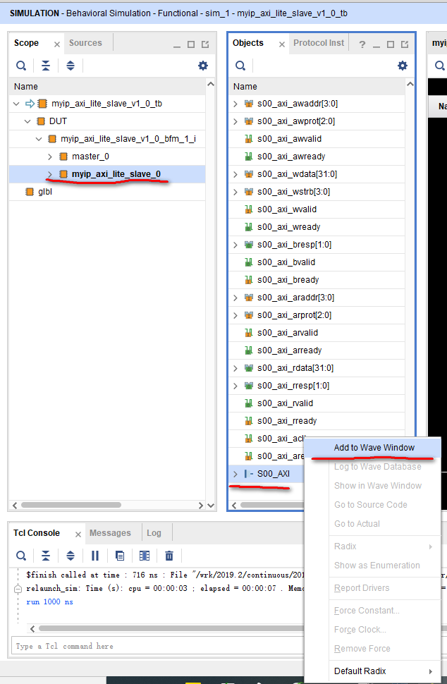
The simulation results are as follows:
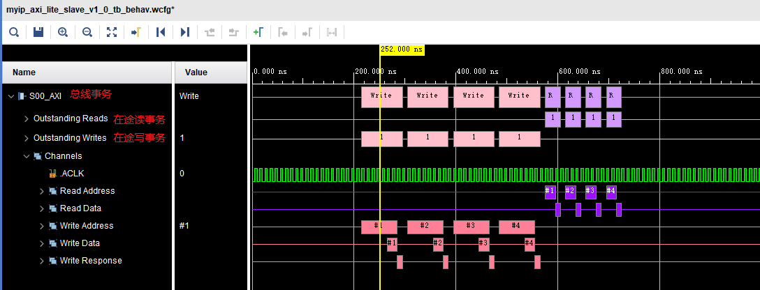
It can be seen that the simulation results are expressed in the form of color bar + character, which is very clear. This is the effect of adding AXI VIP IP.
A total of eight transactions occurred on the axi4 Lite bus: first four consecutive write transactions, and then four read transactions. The following five channels respectively illustrate the handshake operation performed in the channel at this time. Place the mouse on any one of them, and the following information will appear (sequence 1, address 0, etc.):
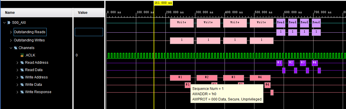
Left click to display the specific transaction flow as follows:
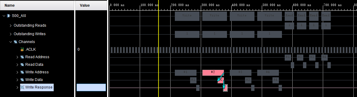
From the arrow in the figure above, we can see the process of a write transaction: write address - write data - write response. Let's look at the process of reading transactions:
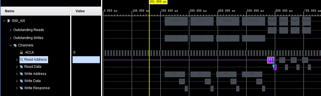
You can see the flow of read transaction: read address - read data.
3.2. Slave interface simulation waveform of slave IP
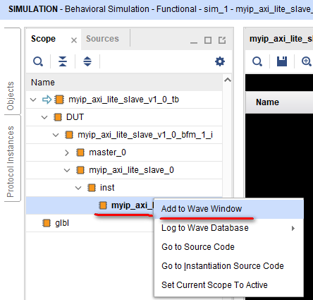
After reading the simulation waveform of axi4 Lite bus, let's look at the simulation waveform of the above specific analysis code (which can be understood as the underlying driver). Add as follows:
Classify the signals according to channel or purpose, and the simulation results are as follows:
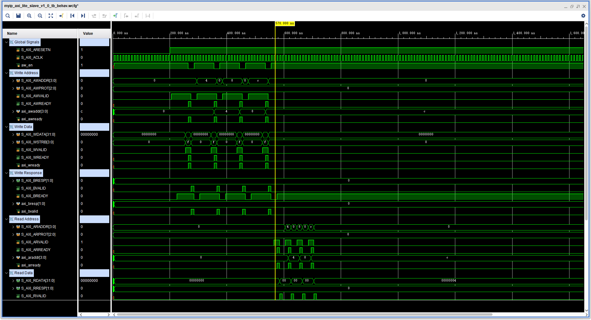
There are many signals. Let's analyze the write transaction as follows:
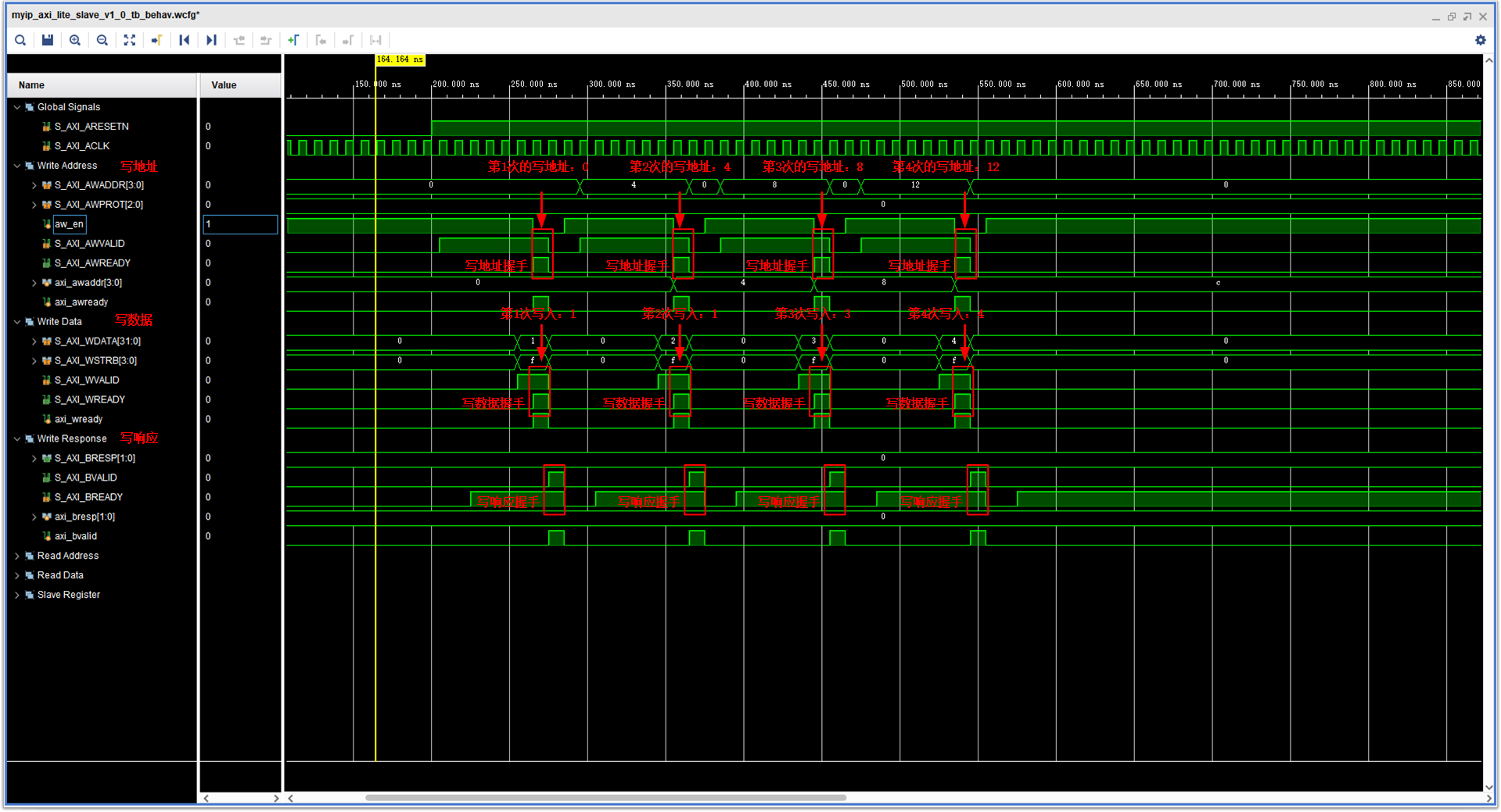
In the figure above, a total of 4 write operations have been performed. The write addresses are 0, 4, 8 and 12 respectively, corresponding to the addresses of the four Slave registers in the Slave. The data written are 1-4 respectively. The handshake process is over. See how the data is written
The of the Slave register is as follows:
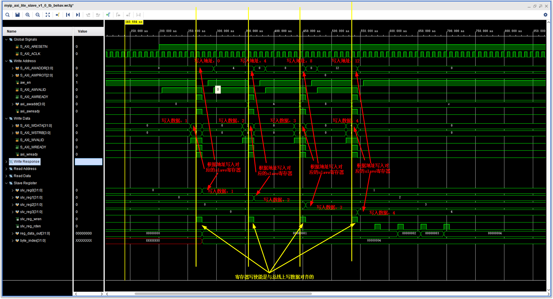
As can be seen from the above figure:
Slave register write enable signal slv_reg_wren is aligned with the write transaction on the bus, so that the data to be written by the bus can be directly written to the slave register;
According to the address to be written, write the data to be written into the corresponding slave register. Specifically, as shown in the figure above, write data 1-4 to the four registers respectively
Let's look at the sequence diagram of read transactions:
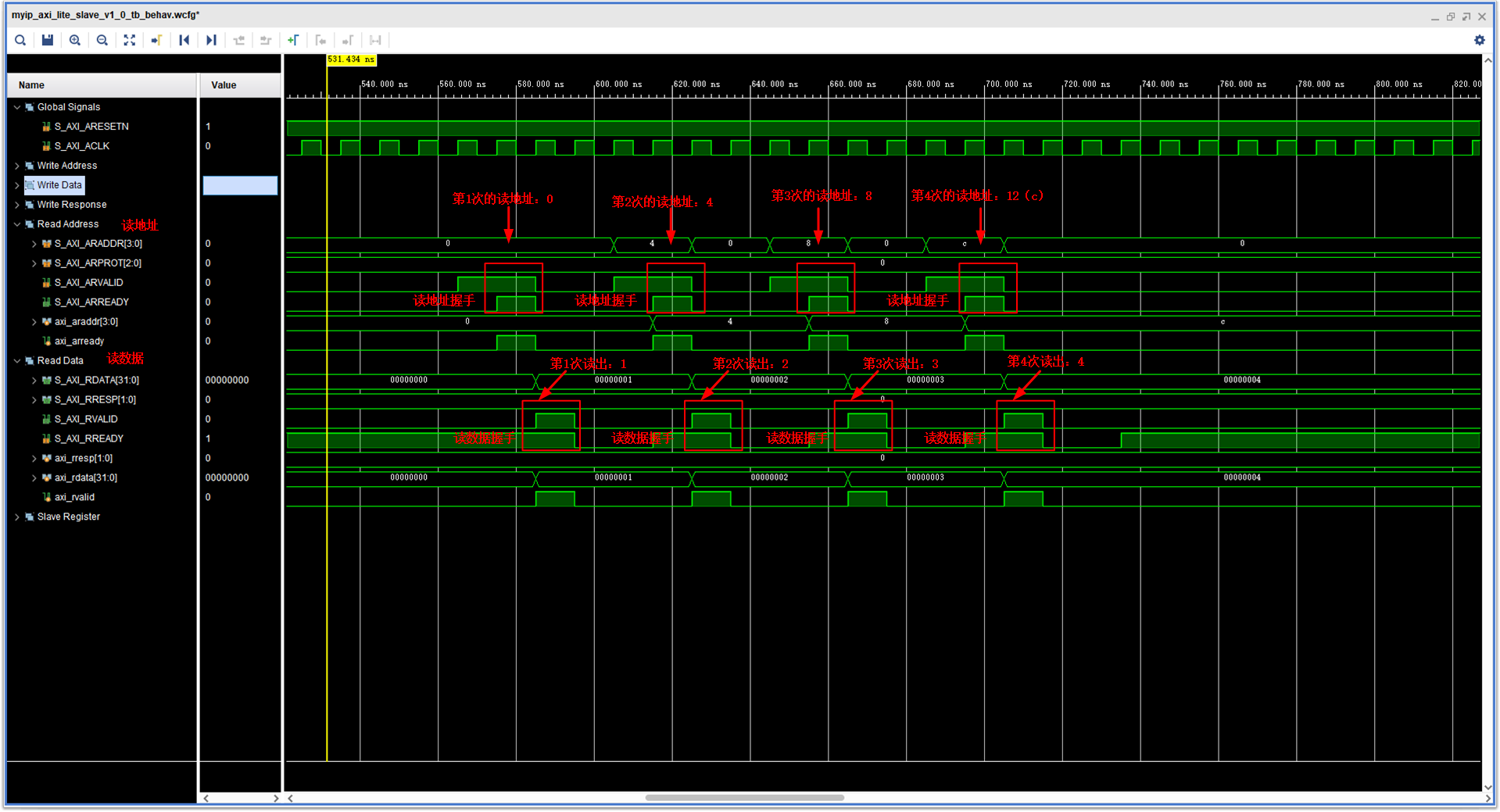
After the handshake is completed, the data 1-4 are read out from the addresses (0, 4, 8, 12) in turn, which is consistent with the previously written data (the data is stored in the slave register of the slave). Next, let's see that the data is read from the slave register:
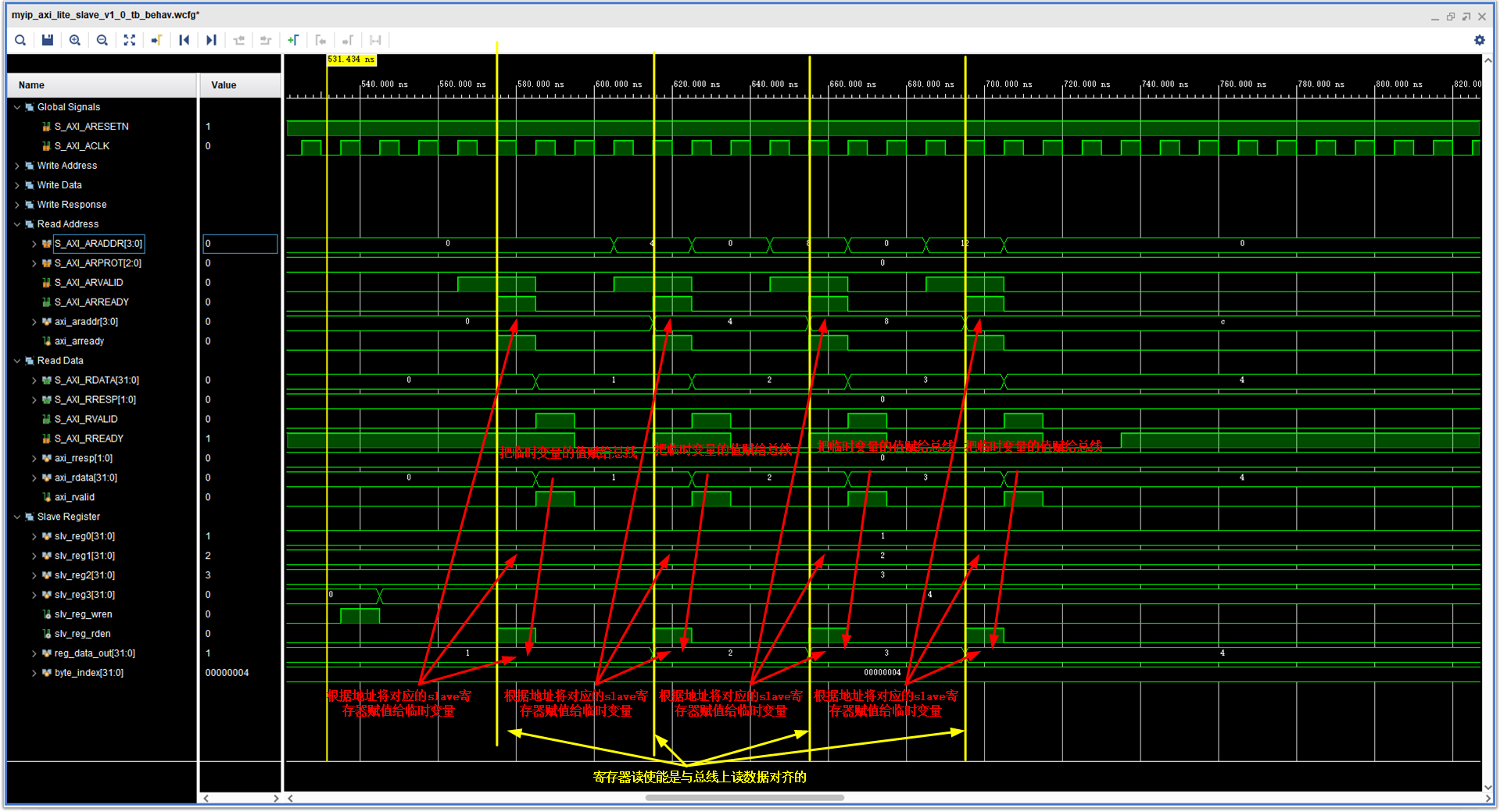
As can be seen from the above figure:
The slave register reads the enable signal slv_reg_rden is aligned with the read transaction on the bus, so that the value of the slave register can be read and assigned to the bus directly. Considering that there is a clock cycle delay in reading the value of the register, the temporary variable reg is used_ data_ Out [31:0] to take a beat and align the timing;
Read data 1-4 from the four slave registers respectively.
4. Other
- It can be seen that the use of axi4 Lite bus is relatively simple. As long as the handshake timing of each channel and the timing relationship of reading and writing are designed. In the next article, we will continue to analyze the code of the Master interface of axi4 Lite bus.
- It's not easy to create. I hope you guys can support it for three times! If there is any mistake, please correct it!
Version information
File: V1.0
No.: 63
Vivado: Vivado 2019.2
Modelsim: None
Quartus II: None