This blog is a brief note of DPDK in simple terms
2.1 introduction to storage system
For packet processing, there are mainly two parts (personal understanding), one is CPU The other is CPU Scheduling of instructions and data to be processed. How to give full play CPU On the basis of performance Cache,Memory, SATA Disk, PCIe Devices (network card, graphics card) and USB Wait for the data in it to be processed more quickly. and CPU The main operation is memory, so this chapter mainly explains the basic knowledge from the perspective of memory.
2.1.1 evolution of system architecture
The classic computer architecture is as follows:
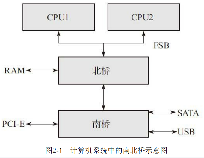
In such a system, it can be seen that all data pass through the North Bridge:
1) The processor needs to access memory through the north bridge.
2) The processor accesses all peripherals through the north bridge.
3) Data exchange between processors also needs to pass through the north bridge.
4) All devices hanging on the south bridge also need to access memory through the north bridge.
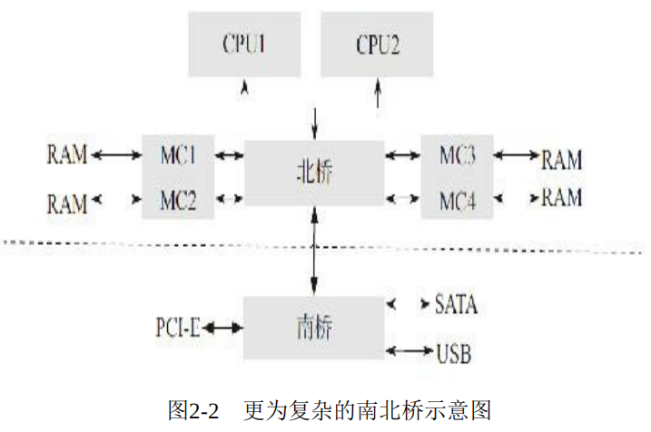
It can be seen that the performance bottleneck of the system is in the North Bridge, and the memory controller is all CPU Service. Therefore, with the following memory improvement system architecture:
Although the memory controller has been improved, the performance bottleneck of Beiqiao has not been improved. Therefore, in order to solve this bottleneck, NUMA (non uniform memory architecture) system is produced, as shown in the following figure:
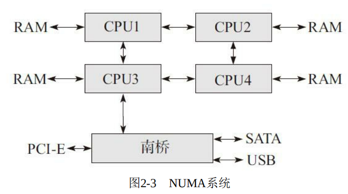
In this system, the bandwidth of memory access is increased by four times, but this architecture also has disadvantages. In this system, the time spent accessing memory is processor dependent. The reason why it is related to the processor is that each processor of the system has Local memory. The time to access the Local memory is very short, while accessing the remote memory, that is, the Local memory of other processors, needs to pass through an additional bus! For a processor, when it wants to access other memory, the light one needs to go through another processor, and the heavy one needs to go through two processors to access non Local memory. Therefore, the "distance" between memory and processor is different, and the access time is also different.
2.1.2 memory subsystem
1)RAM(Random Access Memory): Random access memory
2)SRAM(Static RAM): Static random access memory
3)DRAM(Dynamic RAM): Dynamic random access memory.
4)SDRAM(Synchronous DRAM): Synchronous dynamic random access memory.
5)DDR(Double Data Rate SDRAM): Dual data rate SDRAM.
6)DDR2: Second generation DDR.
7)DDR3: Third generation DDR.
8)DDR4: Fourth generation DDR.
2.2 introduction to cache system
In order to speed up CPU The rate at which memory is accessed, CPU The processing rate is much higher than the memory throughput, so it is proposed Cache The concept of. Cache The main function of is to CPU Instructions to read/Data put Cache Among them, when CPU When necessary, directly from Cache Read in the middle, Cache The read rates are and CPU The rate is consistent, so the read is very fast.
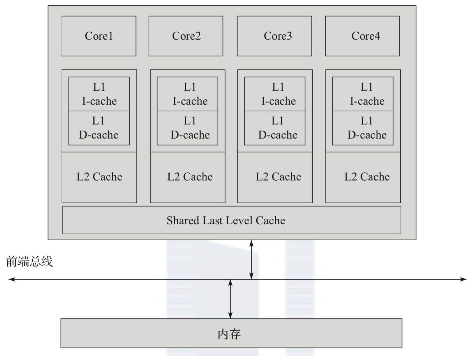
2.2.1 types of cache
Generally speaking, due to the consideration of cost and generation process, Cache There are three levels, one level Cache(L1)Fastest, but smallest capacity, level 3 Cache(L3)The slowest, but the largest capacity. The following figure is a simple example Cache System logic diagram (easy to understand). stay CPU When executing the program, the mechanical code program will be loaded from the disk into the memory, CPU Memory access speed relative to CPU It is much slower for the running rate of, so it is necessary to Cache Prefetch.
2.2.2 TLB Cache
When Cache When missed, CPU You still need to access memory, so you need to access the page table in memory for the first time, convert the virtual address to the physical address, and then access the physical address in memory for the second time to obtain data. Here, the memory is accessed twice. So in order to speed up this rate, we used TLB Cache To cache the page table, so there is no need to access the memory for the first time. It is prefetched first, so you only need to access the memory once, which speeds up the rate of accessing the memory.
2.3 Cache address mapping and transformation
Memory is large, and Cache It is very small, so a mapping mechanism and a blocking mechanism are needed.
Blocking mechanism, that is, Cache And memory exchange data in blocks. The size of blocks is usually limited to the length of data that can be accessed in a storage cycle of memory. Nowadays, the size of mainstream blocks is 64 bytes, so one Cache line It refers to a 64 byte data block.
Mapping algorithm refers to mapping memory address space to Cache Address space. Specifically, it is to load the contents stored in memory into memory according to some rules Cache And establish the memory address and Cache Correspondence between addresses. When content has been loaded into Cache Then, in the actual running process, when the processor needs to access the contents of this data block, it needs to convert the memory address into Cache Address so that in Cache The data block is found in and finally returned to the processor.
Generally, there is full correlation type Cache,Direct correlation Cache Group Association Cache.
2.4 Cache write strategy
Generally speaking, there are the following strategies:

 1. Direct write: the so-called direct write refers to the processor pair Cache While writing, write data to memory. Real time synchronization, but it takes a lot of bus bandwidth.
 2. Writeback: the writeback system uses the Cache line Add a flag to the flag bit field Dirty Flag bit when the processor overwrites a Cache line After, instead of writing it back to memory immediately, the Cache line of Dirty Flag set to 1. When the processor modifies the Cache line And write back Cache During, the table is found Dirty If the bit is already 1, the Cache line The content is written back to the corresponding location in memory, and then the new data is written to Cache Yes. This reduces the occupation of bus bandwidth, but it will cause consistency problems.

There are some different strategies for special memory, including WC(write-combining)and UC(uncacheable)wait.
2.5 Cache prefetching
Cache The reason why the system performance can be improved is that the program execution has locality, that is, temporal locality and spatial locality.

There is an example in the book that introduces the code with the same execution result, but the execution efficiency is very different.
Procedure 1:
for(int i = 0; i < 1024; i++)
{
	for(int j = 0; j < 1024; j++)
	{
		arr[i][j] = num++;
	}
}

Procedure 2:
for(int i = 0; i < 1024; i++)
{
	for(int j = 0; j < 1024; j++)
	{
		arr[j][i] = num++;
	}
}
Program 1 is a sequential assignment, and program 2 is a jump assignment, because Cache Prefetching is memory with similar prefetching space, so program 1 is more efficient.
Software prefetching
Programmers can do some Cache Prefetch instructions (assembly instructions).

 - PREFETCH0 Store data at each level cache among.
 - PREFETCH1 Store data in L1 Cache Extraneous cache.
 - PREFETCH2 Store data in L1,L2 Cache Extraneous cache.
 - PREFETCHNTA And PREFETCH0 Similar, but the data is stored as non temporary data. After using it once, cache It is considered that the data can be eliminated.
again C There are also corresponding interfaces in the language“ mmintrin.h":
void _mm_prefetch(char *p, int i);
*p is the prefetch address, and i corresponds to the corresponding prefetch instruction.
DPDK also has prefetch functions, which are not described in detail in the book, so you need to read them in detail later.
while (nb_rx < nb_pkts)
{
	rxdp = &rx_ring[rx_id]; //Read receive descriptor
	staterr = rxdp->wb.upper.status_error; //Check whether any message is received
	if (!(staterr & rte_cpu_to_le_32(IXGBE_RXDADV_STAT_DD))) break;
	rxd = *rxdp;
	//Allocate data buffer
	nmb = rte_rxmbuf_alloc(rxq->mb_pool);
	nb_hold++;
	//Read control structure
	rxe = &sw_ring[rx_id];
	......
	rx_id++;
	if (rx_id == rxq->nb_rx_desc) rx_id = 0;
	//Prefetch the next control structure
	mbuf rte_ixgbe_prefetch(sw_ring[rx_id].mbuf);
	//Prefetch receive descriptor and control structure pointer
	if ((rx_id & 0x3) == 0)
	{
		rte_ixgbe_prefetch(&rx_ring[rx_id]);
		rte_ixgbe_prefetch(&sw_ring[rx_id]);
	}
	......
	//Prefetch message
	rte_packet_prefetch((char *)rxm->buf_addr + rxm->data_off);
	//The information read by the reception descriptor is stored in the control structure mbuf
	rxm->nb_segs = 1;
	rxm->next = NULL;
	rxm->pkt_len = pkt_len;
	rxm->data_len = pkt_len;
	rxm->port = rxq->port_id;
	......
	rx_pkts[nb_rx++] = rxm;
}
2.6 Cache consistency
about Cache line There are two problems in reading and writing:
1)The starting address of the data structure or data buffer is Cache Line Aligned? If not, even if the size of the data area is less than Cache Line,Then you also need to occupy two Cache entry;And, suppose the first Cache Line The first half belongs to another data structure and is being processed by another processor core, then when both cores modify the Cache Line To write back to their respective levels Cache,How do I synchronize data when I'm ready to send it to memory? After all, each core only modifies the Cache Line Part of.
 2)Suppose that the starting address of the data structure or data buffer is Cache Line Aligned, but multiple cores read and write the memory at the same time. How to solve the conflict when writing back to the memory at the same time?
Consistency protocol
MESI Agreement to solve Cache The issue of consistency will not be repeated here.
Cache line alignment
DPDK The alignment is declared when the data structure or data buffer is defined, DPDK This is how many structures are defined.
struct rte_ring_debug_stats
{
	uint64_t enq_success_bulk;
	uint64_t enq_success_objs;
	uint64_t enq_quota_bulk;
	uint64_t enq_quota_objs;
	uint64_t enq_fail_bulk;
	uint64_t enq_fail_objs;
	uint64_t deq_success_bulk;
	uint64_t deq_success_objs;
	uint64_t deq_fail_bulk;
	uint64_t deq_fail_objs;
} __rte_cache_aligned;

#define RTE_CACHE_LINE_SIZE 64
#define __rte_cache_aligned __attribute__((__aligned__(RTE_CACHE_LINE_SIZE)))
The second is to access the network port, because the network card generally has the ability of multiple queues, DPDK A separate receive queue or send queue will be prepared for each core. An example in the book is as follows:
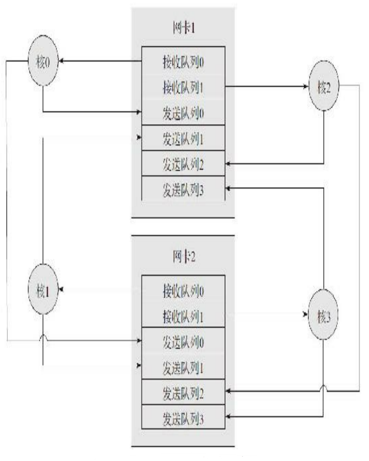
In actual use, you need to check whether the network card has been bound to a core to prevent it. The program and the network card are not bound to a core!
2.7 TLB and large pages
The table lookup sequence for converting a logical address to a physical address is generally as follows:

 1. According to bit bit[31: 22]Add register CR3 The base address of the stored page directory table, obtain the physical address of the corresponding table item in the page directory table, read the memory, and obtain the content of the table item from the memory, so as to obtain the base address of the next level page table.
 2. According to bit bit[21: 12]Add the page table base address obtained in the previous step to the page table, obtain the physical address of the corresponding table item in the page table, read the memory, and obtain the content of the table item from the memory, so as to obtain the base address of the content page.
 3. According to bit[11: 0]Add the base address of the content page obtained in the previous step to obtain the accurate physical address, and read the content to obtain the real content.
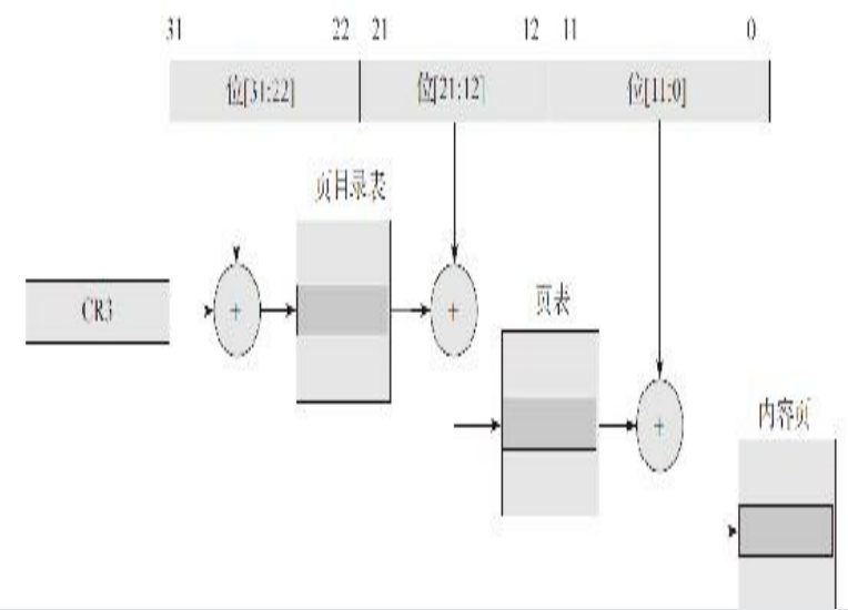
TLB saves the correspondence between [31:12] and page frame number in its own Cache, greatly reducing the first and second table lookup time, so as to speed up the access of program memory content.
However, since the size of TLB under linux is 4KB, in order to reduce the miss rate, you need to use large pages, 2MB or 1GB, etc. How to do this is not described in detail here, but it needs to be set.
DDIO(Data Direct I/O)
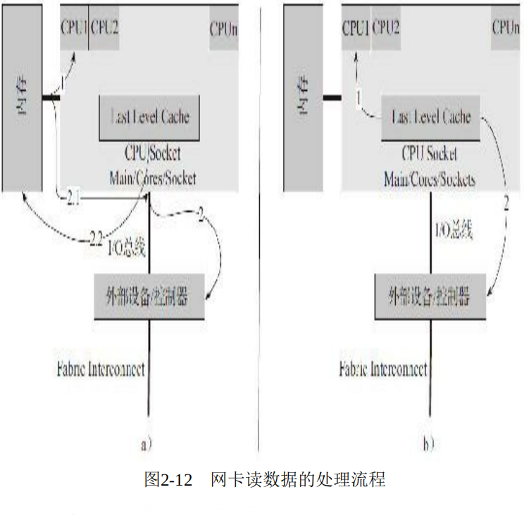
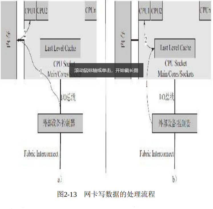
DDIO It is generated to avoid saving data to memory, even if the external network card and CPU adopt LLC Cache Direct data exchange bypasses the relatively slow component of memory.
In this way, it increases CPU Speed of processing network messages (reduced) CPU And the waiting time of the network card for memory), which reduces the processing delay of the network message at the server. This also poses a problem because network messages are stored directly in the LLC Cache In, this greatly increases the demand for its capacity, so in Intel's E5 In the processor family, the LLC Cache Increased capacity to 20 MB.
The following is a comparison of the processing flow of network card reading and writing, a No DDIO Technology, b Is adopted DDIO Technology.
2.9 NUMA system
NUMA The system needs to be considered PCIe Where is the device CPU Under cluster, to DPDK Bind to this CPU Under the cluster, the processing delay can be optimized. Otherwise need CPU If the transmission is carried out, the delay will increase greatly.