1. D trigger
definition:
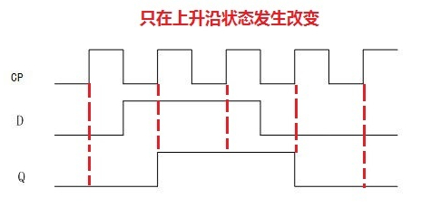
D flip-flop is an information storage device with memory function and two stable states. The flip-flop has two stable states, namely "0" and "1". Under the action of certain external signals, it can flip from one stable state to another. The edge triggered D flip-flop is explained here. The D flip-flop flips at the leading edge of the clock pulse CP (positive jump 0 → 1). The secondary state (next state) of the flip-flop depends on the state of the d end before the rising edge of the pulse of CP, that is, the secondary state Q=D. Therefore, it has two functions: setting 0 and setting 1. Since the circuit has the function of maintaining blocking during CP=1 (i.e. the output of the trigger remains unchanged), during CP=1, the data state of D terminal changes and will not affect the output state of the trigger, so the possibility of interference of edge D trigger is reduced.
Menu:
| D | CLK | Q | QN |
|---|---|---|---|
| 0 | Rising edge of clock | 0 | 1 |
| 1 | Falling edge of clock | 1 | 0 |
| x | 0 | last Q | last QN |
| x | 1 | last Q | last QN |
Synchronous reset and asynchronous reset
(1) Synchronous reset:
As the name suggests, synchronous reset means that the reset signal can be effective only when the rising edge of the clock comes. Otherwise, the system reset cannot be completed. Verilog is used to describe as follows:
always @ (posedge clk) begin
	if (!Rst_n)
		...
end
(2) Asynchronous reset:
It means that the system will be reset as long as the reset signal is valid regardless of whether the clock edge arrives or not. Verilog is used to describe as follows:
always @ (posedge clk or negedge Rst_n) begin
	if (!Rst_n)
		...
end
practice:
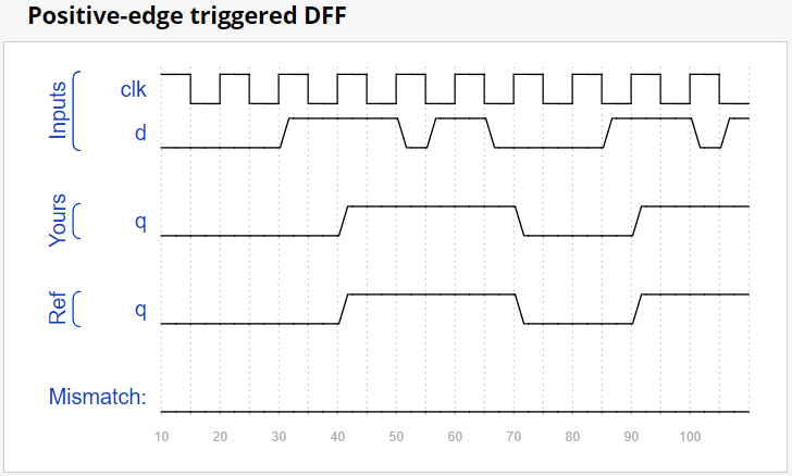
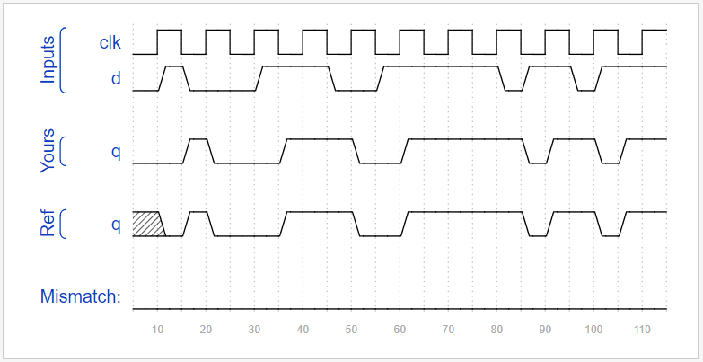
Create a single D trigger.
Note: non blocking assignment is often used in the always block of timing.
Code implementation:
module top_module (
    input clk,
    input d,
    output reg q );

    always@(posedge clk) begin
         q <= d;
    end

endmodule
Verification results:
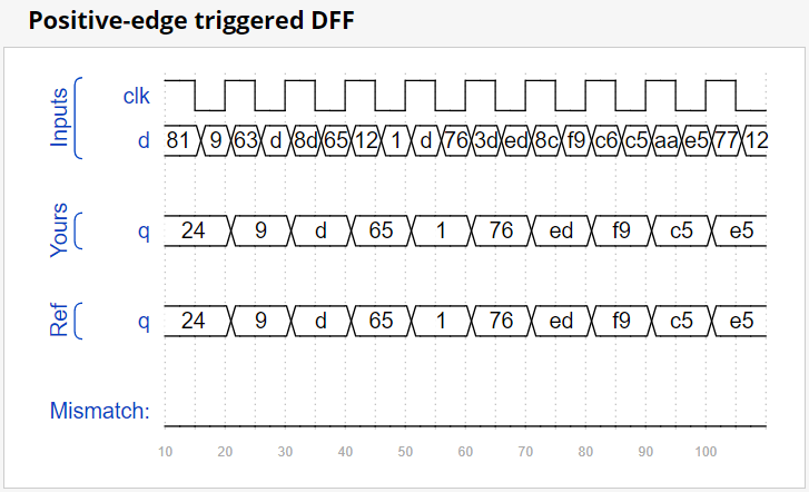
2. 8 D flip flops
Create 8 D flip flops, each triggered by the rising edge of the clock.
Code implementation:
module top_module (
    input clk,
    input [7:0] d,
    output [7:0] q
);
    always@(posedge clk) begin
        q <= d;
    end

endmodule
Verification results:
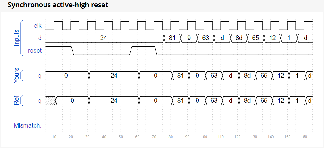
3. D trigger with synchronous reset (rising edge trigger)
Create 8 d flip flops with active high synchronous reset. All d flip flops are triggered by the rising edge of clk.
Code implementation:
module top_module (
    input clk,
    input reset,
    input [7:0] d,
    output [7:0] q
);

    always@(posedge clk) begin
        if(!reset)
            q <= d;
    	else
            q <= 8'b0;
    end

endmodule
Verification results:
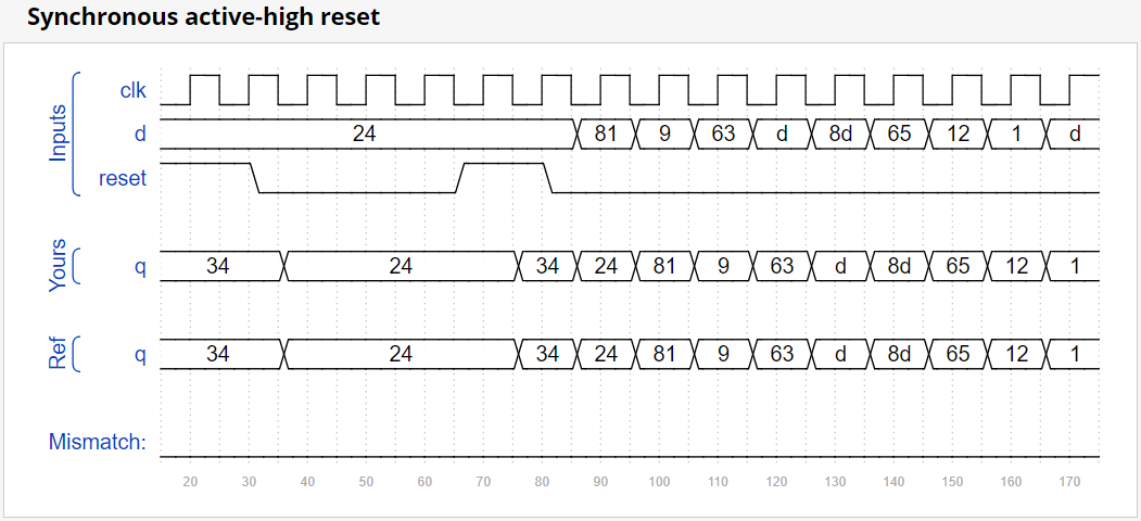
4. D trigger with synchronous reset (falling edge trigger)
Create 8 D flip flops with active high synchronization reset. The trigger must be reset to 0x34 instead of 0. All D triggers shall be triggered by the falling edge of clk.
Code implementation:
module top_module (
    input clk,
    input reset,
    input [7:0] d,
    output [7:0] q
);
    always@(negedge clk) begin
        if(!reset)
            q <= d;
        else
            q <= 8'h0x34;
    end

endmodule
Verification results:
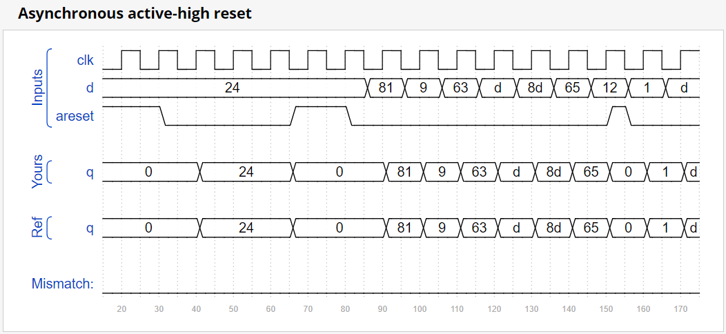
5. D trigger with asynchronous reset
Create 8 D flip flops with active high asynchronous reset. All D triggers shall be triggered by the rising edge of clk.
Code implementation:
module top_module (
    input clk,
    input areset,
    input [7:0] d,
    output [7:0] q
);

    always@(posedge clk or posedge areset) begin
        if(areset)
            q <= 8'b0;
        else
            q <= d;
    end

endmodule
Verification results:
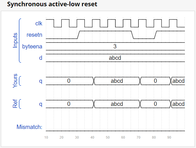
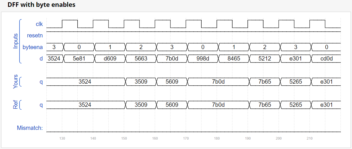
6. D trigger with byte enable
To create 16 D triggers, sometimes we only need to modify the values in some triggers. The byte enable signal controls which byte of the 16 registers in the current clock cycle needs to be modified. byteena[1] controls the high byte d[15:8], while byteena[0] controls the low byte d[7:0].
resetn is a synchronous, low-level effective reset signal.
All D flip flops are triggered by the rising edge of the clock.
Code implementation:
module top_module (
    input clk,
    input resetn,
    input [1:0] byteena,
    input [15:0] d,
    output [15:0] q
);

    always@(posedge clk) begin
        if(resetn) begin
            if(byteena[1])
                q[15:8] <= d[15:8];
            else
                q[15:8] <= q[15:8];

            if(byteena[0])
                q[7:0] <= d[7:0];
            else
                q[7:0] <= q[7:0];
        end

        else
            q <= 16'b0;
    end

endmodule
Verification results:
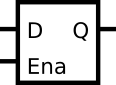
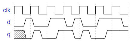
7. D latch
Implement the following circuit (latch).
Code implementation:
module top_module (
    input d,
    input ena,
    output q);

    always@(*) begin
    if(ena)
      q = d;
    else
      q = q;
    end

endmodule
Verification results:
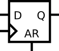
8. D trigger 1
Implement the following circuit.
Code implementation:
module top_module (
    input clk,
    input d,
    input ar,   // asynchronous reset
    output q);

    always@(posedge clk or posedge ar) begin
        if(ar)
            q <= 1'b0;
        else
            q <= d;
    end

endmodule
Verification results:
9. D trigger 2
The following circuits are implemented:
Code implementation:
module top_module (
    input clk,
    input d,
    input r,   // synchronous reset
    output q);

    always@(posedge clk) begin
        if(!r)
            q <= d;
        else
            q <= 1'b0;
    end

endmodule
Verification results:
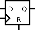
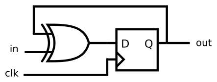
10. D trigger + gate circuit
The following circuits are implemented:
Code implementation:
module top_module (
    input clk,
    input in,
    output out);

    always@(posedge clk) begin
        out <= in ^ out ;
    end

endmodule
Verification results:
11. Multiplexer + D trigger 1
Consider the following sequential circuits:
Suppose you want to implement layered Verilog code for this circuit, using three instances of a sub module with a trigger and multiplexer. Write a sub module called top for this sub module_ Module (including a trigger and multiplexer).
Code implementation:
Method 1: if else statement implementation
module top_module (
	input clk,
	input L,
	input r_in,
	input q_in,
	output reg Q);

    always@(posedge clk) begin
        if(L)
            Q <= r_in;
        else
            Q <= q_in;
    end

endmodule
Method 2: a? b: c statement implementation
module top_module (
	input clk,
	input L,
	input r_in,
	input q_in,
	output reg Q);

    always@(posedge clk) begin
       Q <= L?r_in:q_in;
    end

endmodule
Verification results:
12. Multiplexer + D trigger 2
Consider the n-bit shift register in the figure below:
Write a program called top for one phase of the circuit_ Module Verilog module, including trigger and multiplexer.
Code implementation:
Method 1:
module top_module (
    input clk,
    input w, R, E, L,
    output Q
);

    always@(posedge clk) begin
        Q <= L ? R: ( E ? w : Q);
    end

endmodule
Method 2:
module top_module (
    input clk,
    input w, R, E, L,
    output Q
);

    always@(posedge clk) begin
        case({E,L})
       	 2'b00: Q <= Q;
         2'b01: Q <= R;
         2'b10: Q <= w;
         2'b11: Q <= R;
         default: Q <= Q;
        endcase
    end

endmodule
Verification results:
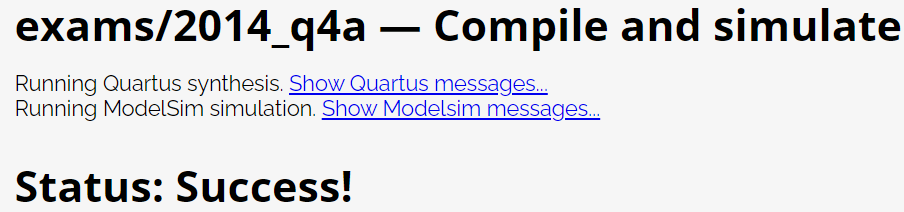
13. Multiple D flip flops + gates
Given the finite state machine circuit shown in the figure, it is assumed that the D trigger is initially reset to zero before the machine starts.

Code implementation:
module top_module (
    input clk,
    input x,
    output z
);

    reg Q1,Q2,Q3;
    always@(posedge clk) begin
       Q1 <= x ^ Q1;
       Q2 <= x & ~Q2;
       Q3 <= x | ~Q3;
    end

    assign  z = ~(Q1|Q2|Q3);

endmodule
Verification results:
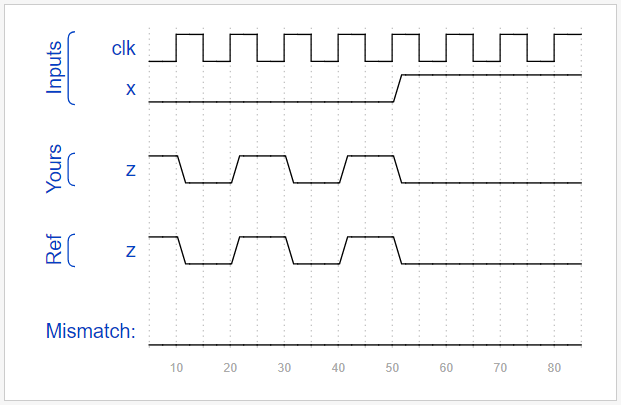
14. Create circuit from truth table
JK Trigger has the following truth table. Only D flip flops and logic gates are used to implement JK flip flops.
Note: Qold is the output of the D flip-flop before the rising edge of the clock.
| J | K | Q |
|---|---|---|
| 0 | 0 | Qold |
| 0 | 1 | 0 |
| 1 | 0 | 1 |
| 1 | 1 | ~Qold |
Code implementation:
module top_module (
    input clk,
    input j,
    input k,
    output Q);

    always@(posedge clk) begin
        case({j,k})
            2'b00: Q <= Q;
            2'b01: Q <= 1'b0;
            2'b10: Q <= 1'b1;
            2'b11: Q <= ~Q;
            default: Q <= Q;
        endcase
    end

endmodule
Verification results:
15. Pulse edge detection 1
Pulse edge detection principle
Characteristics of pulse edge: the levels on both sides have changed.
If the falling edge is detected, it is that the high level changes to the low level.
If the rising edge is detected, the low level changes to high level.
If the edge of the pulse is detected, it only needs to do XOR operation on the incoming signals, that is, if the two levels are different, it is the edge.
Idea:
A register is designed to receive the detected signal; If {advanced reg, backward reg}=2'b10, it is the falling edge;
If {advanced reg, backward reg}=2'b01, it is the rising edge.
Note: using multiple registers can better detect edges and prevent interference pulses. See the following example for details:
always @ (posedge clk or negedge rst_n) begin
    if(!rst_n) begin
        rs232_rx0 <= 1'b0;
        rs232_rx1 <= 1'b0;
        rs232_rx2 <= 1'b0;
        rs232_rx3 <= 1'b0;
	end
    else begin
        rs232_rx0 <= rs232_rx;
        rs232_rx1 <= rs232_rx0;
        rs232_rx2 <= rs232_rx1;
        rs232_rx3 <= rs232_rx2;
    end
end
//This method can filter 20-40ns burrs
assign neg_rs232_rx = rs232_rx3 & rs232_rx2 & ~rs232_rx1 & ~rs232_rx0;
Easy to analyze, backward signal rs232_rx0,rs232_rx1, all must be 0, and the advanced signal rs232_rx3 ,rs232_rx2 must be 1, neg_rs232_rx will be 1. Then it is judged as the falling edge.
practice:
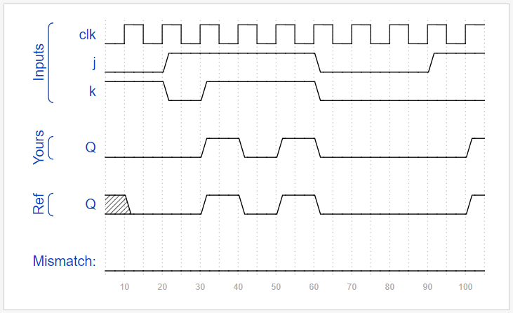
For each bit of the 8-bit vector, detect when the input signal changes from 0 of one clock cycle to 1 of the next clock cycle (positive edge detection). The output bit should be in the cycle after 0 to 1 conversion, as shown in the following diagram:
Code implementation:
module top_module (
    input clk,
    input [7:0] in,
    output [7:0] pedge
);

    reg [7:0] temp;
    always@(posedge clk) begin
        temp <= in;
        pedge <= in & ~temp;
    end

endmodule
Verification results:
16. Pulse edge detection 2
For each bit of the 8-bit vector, detect when the input signal changes from one clock cycle to the next clock cycle (detect the edge of the pulse). The output bit should be in the cycle after conversion.
Code implementation:
module top_module (
    input clk,
    input [7:0] in,
    output [7:0] anyedge
);
    reg [7:0] temp;
    always@(posedge clk) begin
        temp <= in;
        anyedge <= in ^ temp;
    end

endmodule
Verification results:
17. Edge capture register
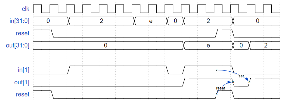
For each bit in the 32-bit vector, when the input signal changes from 1 of one clock cycle to 0 of the next clock cycle, "capture" means that the output will remain 1 until it is reset (synchronous reset).
Each output bit behaves like an SR trigger: the output bit should be set (to 1) in the cycle after the 1 to 0 conversion occurs. When reset to high, the output bit should be reset at the positive clock edge (0). If the above two events occur at the same time, reset has priority.
In the last four cycles of the following example waveform, the "reset" event occurs one cycle earlier than the "set" event, so there is no conflict here.
Code implementation:
Method 1:
module top_module (
    input clk,
    input reset,
    input [31:0] in,
    output [31:0] out
);

    reg [31:0] temp;
    always@(posedge clk) begin
        temp <= in;
        if(reset)
            out <= 32'b0;
        else
            out <= ~in & temp | out;
    end

endmodule
Method 2:
module top_module (
    input clk,
    input reset,
    input [31:0] in,
    output [31:0] out
);

   reg [31:0] temp_in;
    reg [31:0] state;
    integer i;

    always @(posedge clk) begin
        temp_in <= in;
        for(i=0;i<32;i++) begin
            case({temp_in[i] & ~in[i],reset})
                2'b10:out[i]<=1'b1;
                2'b11:out[i]<=1'b0;
                2'b01:out[i]<=1'b0;
                default:out[i]<=out[i];
            endcase
        end
    end

endmodule
Verification results:
18. Clock double edge trigger
Build a circuit with function similar to double edge trigger trigger:
Code implementation:
Method 1:
module top_module (
    input clk,
    input d,
    output q
);

    reg q1,q2;

    always@(posedge clk) begin
        q1 <= d;
    end

    always@(negedge clk) begin
        q2 <= d;
    end

    assign q = clk? q1 : q2;

endmodule
Method 2:
module top_module (
    input clk,
    input d,
    output q
);

    reg q1,q2;

    always@(posedge clk) begin
        q1 <= d ^ q2;
    end

    always@(negedge clk) begin
        q2 <= d ^ q1;
    end

    assign q = q1 ^ q2;

endmodule
Verification results:
Compared with method 1, method 2 uses less clk signal for selection, which can avoid burrs. Method 2 is recommended for bilateral detection.
reference material: D trigger, synchronous and asynchronous reset, pulse edge detection.